HAL Id: hal-01527602
https://hal.archives-ouvertes.fr/hal-01527602
Submitted on 24 May 2017
HAL is a multi-disciplinary open access
archive for the deposit and dissemination of
sci-entific research documents, whether they are
pub-lished or not. The documents may come from
teaching and research institutions in France or
abroad, or from public or private research centers.
L’archive ouverte pluridisciplinaire HAL, est
destinée au dépôt et à la diffusion de documents
scientifiques de niveau recherche, publiés ou non,
émanant des établissements d’enseignement et de
recherche français ou étrangers, des laboratoires
publics ou privés.
High-Efficiency Fiber-Chip Surface Grating Couplers
D Benedikovic, C Alonso-Ramos, L Vivien, P Cheben, J Schmid, S Wang,
D-X Xu, B Lamontagne, J Lapointe, S Janz, et al.
To cite this version:
D Benedikovic, C Alonso-Ramos, L Vivien, P Cheben, J Schmid, et al.. High-Efficiency Fiber-Chip
Surface Grating Couplers. SPIE Photonics North, 2016, Quebec city, Canada. �hal-01527602�
High-Efficiency Fiber-Chip Surface Grating Couplers
D. Benedikovic
1,*, C. Alonso-Ramos
1, L. Vivien
1, P. Cheben
2, J. H. Schmid
2, S. Wang
2, D.-X. Xu
2, B. Lamontagne
2,
J. Lapointe
2, S. Janz
2, R. Halir
3, A. Ortega-Moñux
3, J.-G. Wangüemert-Pérez
3, I. Molina-Fernández
3, J. M. Fédéli
4, M.
Dado
51Institut d’Electronique Fondamentale, Université Paris Sud, CNRS, UMR 8622, Université Paris-Saclay, Bat. 220, Orsay Cedex,
France
2National Research Council Canada, Information and Communication Technologies, Ottawa, Ontario, Canada 3Dpto. de Ingeniería Comunicaciones, ETSI Telecomunicación, Universidad de Málaga, Málaga, Spain
4
CEA-LETI, Minatec, CEA-Grenoble, France
5University of Žilina, Dept. of Telecommunications and Multimedia, Žilina, Slovakia *[email protected]
Abstract— We report our latest advances in development of
high-efficiency fiber-chip surface grating couplers with refractive index engineered subwavelength structures. We present different experimental demonstrations of high-performance grating-coupled optical interfaces, developed on the standard 220-nm silicon-on-insulator technology in the near-infrared wavelengths.
Keywords—Grating couplers; refractive index engineering; subwavelength grating; silicon-on-insulator; silicon photonics
I. INTRODUCTION
The coupling of light to or from microphotonic circuits is still one of the major practical challenges of silicon technology. The surface grating couplers afford effective approach to interface silicon chips, with relaxed alignment tolerances, wafer scale testing capability, and compatibility with integration and packaging technologies [1-5].
II. SINGLE-ETCH GRATING COUPLERS
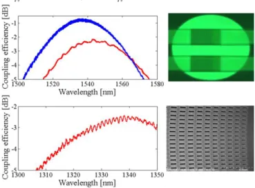
We reported a set of subwavelength index engineered apodized grating couplers that desired only one fabrication step, while demonstrating the state-of-the-art fiber-chip coupling performance. In particular, we experimentally shown that by optimizing the thin film interference from the bottom oxide cladding, the peak efficiency of up to -2.2 dB and -2.5 dB are achieved near 1.55 µm and 1.3 µm wavelengths, as shown in Fig. 1 (red curves) [1-3]. The couplers are implemented on a standard silicon-on-insulator (SOI) wafer with 220-nm-thick layer. We also demonstrated the first sub-decibel fiber-chip coupling efficiency of -0.7 dB (blue curve in Fig. 1) in this platform by utilizing the backside wafer processing, followed by metal mirror deposition [2]. The optical micrograph and scanning electron microscope (SEM) images of fabricated couplers are shown in Fig. 1.
III. DUAL-ETCH GRATING COUPLERS
We also developed a flexible dual-etch fiber-chip grating coupler with an extraordinary intrinsic directionality of 95%, independently on the buried oxide thickness [4]. The grating geometry comprises interleaved deep and shallow etched trenches and a short subwavelength index-matching section to
reduce reflections [5]. The grating coupler was realized on regular SOI with 220-nm layer over 3-μm buried oxide. The measured coupling efficiency is -1.3 dB, as shown in Fig. 2, altogether with the SEM image.
Fig. 1 Measured coupling efficiencies as a function of wavelength of single-etch apodized grating couplers, with and without metal reflector underneath. Optical micrograph and SEM images of fabricated structures.
Fig. 2 Measured coupling efficiency as a function of wavelength of dual-etch coupler with interleaved deep and shallow etched trenches. SEM image of fabricated device.
IV. REFERENCES
[1] D. Benedikovic, et al., Laser Photon Rev 8(6), 93-97, 2014. [2] D. Benedikovic, et al., Opt. Express 23(17), 22628-22635, 2015. [3] D. Benedikovic, et al., Opt. Express (to be submitted), 2016. [4] C. Alonso-Ramos, et al. Opt. Lett. 39(19), 5351-5354, 2014. [5] D. Benedikovic, et al., Opt. Lett. 40(18), 4190-4193, 2015.
This work was supported by the European Research Council (ERC) under the European Union’s Horizon 2020 research and innovation program (ERC POPSTAR - grant agreement No 647342).