HAL Id: tel-01661587
https://tel.archives-ouvertes.fr/tel-01661587
Submitted on 12 Dec 2017
HAL is a multi-disciplinary open access
archive for the deposit and dissemination of sci-entific research documents, whether they are pub-lished or not. The documents may come from teaching and research institutions in France or abroad, or from public or private research centers.
L’archive ouverte pluridisciplinaire HAL, est destinée au dépôt et à la diffusion de documents scientifiques de niveau recherche, publiés ou non, émanant des établissements d’enseignement et de recherche français ou étrangers, des laboratoires publics ou privés.
Molecular beam epitaxy growth and optical
characterization of GaN/AlGaN nanowire
heterostructures emitting in the ultraviolet
Matthias Belloeil
To cite this version:
Matthias Belloeil. Molecular beam epitaxy growth and optical characterization of GaN/AlGaN nanowire heterostructures emitting in the ultraviolet. Materials Science [cond-mat.mtrl-sci]. Uni-versité Grenoble Alpes, 2017. English. �NNT : 2017GREAY021�. �tel-01661587�
THÈSE
Pour obtenir le grade de
DOCTEUR DE LA
COMMUNAUTÉ UNIVERSITÉ GRENOBLE ALPES
Spécialité : PHYSIQUE DES MATERIAUX
Arrêté ministériel : 25 mai 2016
Présentée par
Matthias BELLOEIL
Thèse dirigée par Bruno DAUDIN, CEA et co-dirigée par Bruno GAYRAL, CEA
préparée au sein du Laboratoire PHotonique, ELectronique et
Ingéniérie QuantiqueS
dans l'École Doctorale Physique
Croissance par épitaxie par jets moléculaires
et caractérisation optique d'hétérostructures
de nanofils GaN/AlGaN émettant dans
l'ultraviolet
Molecular beam epitaxy growth and optical
characterization of GaN/AlGaN nanowire
heterostructures emitting in the ultraviolet
Thèse soutenue publiquement le 12 mai 2017, devant le jury composé de :
Monsieur ENRIQUE CALLEJA PARDO
PROFESSEUR, UNIV. POLYTECHNIQUE DE MADRID - ESPAGNE, Rapporteur
Monsieur RAPHAËL BUTTE
MAITRE D'ENSEIGNEMENT ET DE RECHERCHE, ECOLE POLYTECH. FEDERALE LAUSANNE SUISSE, Rapporteur
Monsieur PIERRE LEFEBVRE
DIRECTEUR DE RECHERCHE, CNRS DELEGATION LANGUEDOC-ROUSSILLON, Examinateur
Monsieur JOËL LEYMARIE
PROFESSEUR, UNIV. BLAISE PASCAL, CLERMONT-FERRAND, Examinateur
Monsieur HUBERT RENEVIER
1
Contents
Contents ... 1 Acknowledgements ... 5 Main acronyms ... 7 0. Introduction ... 100.1 Brief history of III-Nitride semiconductor research: from prehistory to the recent interest for nanowires ... 10
0.2 Context and motivations of the present research ... 12
0.3 Organization of the manuscript ... 15
0.4 Collaborations ... 15
1. Properties and growth of standard III-Nitride semiconductors ... 17
1.0 Introduction ... 17
1.1 Structural properties of III-Nitride semiconductors ... 17
1.1.1 Crystal structures of nitride materials ... 17
1.1.2 Polarity in wurtzite nitrides ... 21
1.1.3 Spontaneous and piezoelectric polarization in wurtzite nitrides ... 22
1.2 Electronic properties of III-Nitride semiconductors ... 23
1.2.1 Band structure of bulk wurtzite III-Nitride binary crystals ... 23
1.2.1.1 Bandgap of bulk wurtzite nitride binary crystals... 23
1.2.1.2 Other electronic transitions in bulk wurtzite nitride binaries ... 26
1.2.1.3 Effect of external parameters on the band structure of bulk nitride binaries ... 31
1.2.2 Peculiarities of nitride ternary alloys ... 34
1.2.2.1 Bandgap of ternary alloys ... 34
1.2.2.2 Broadening of emission for nitride ternary alloys ... 35
1.2.2.3 Stokes shift in nitride ternary alloys ... 36
1.2.3 Effect of the dimensionality of nitride objects ... 38
1.2.3.1 Effects intrinsic to carrier quantum confinement in nitrides ... 38
1.2.3.2 A consequence of the nitride peculiar polarization: the quantum-confined Stark effect (QCSE) ... 41
1.2.3.3 The case of nitride nanowires ... 43
1.2.3.4 Effect of excitation in nitride quantum heterostructures ... 45
1.3 Growth of III-Nitride semiconductors ... 48
1.3.1 Main existing epitaxial growth techniques ... 49
1.3.2 Main epitaxial growth mechanisms ... 50
1.3.2.1 Main kinetic and surface phenomena ... 50
Contents
2
1.3.2.3 Main epitaxial growth modes ... 53
2. Experimental methods ... 56
2.0 Introduction ... 56
2.1 Our growth technique: plasma-assisted molecular beam epitaxy (PA-MBE) ... 56
2.1.1 Presentation of the molecular beam epitaxy setup ... 56
2.1.1.1 The molecular beam epitaxy chamber ... 56
2.1.1.2 The effusion and plasma cells ... 57
2.1.1.3 The regulation of sample temperature ... 58
2.1.1.4 In situ monitoring with reflection high energy electron diffraction (RHEED) ... 60
2.1.2 Preparation of substrates and calibrations ... 63
2.1.2.1 Preparation of substrates... 63
2.1.2.2 RHEED calibration of growth temperature with a Si (111) wafer ... 64
2.1.2.3 RHEED calibration of atomic fluxes ... 67
2.1.3 GaN nanowire growth ... 69
2.1.3.1 GaN nanowire growth on Si (111) ... 69
2.1.3.2 GaN nanowire growth on AlN buffer ... 73
2.1.4 AlxGa1-xN nanowire growth ... 74
2.1.4.1 AlGaN nanowire growth peculiarities ... 74
2.1.4.2 Additional calibration for GaN and AlxGa1-xN nanowire growth ... 77
2.2 Structural characterization techniques ... 82
2.2.1 Electron microscopy ... 82
2.2.1.1 Scanning electron microscopy (SEM) ... 85
2.2.1.2 Scanning transmission electron microscopy (STEM) ... 86
2.2.1.3 Energy-dispersive X-ray (EDX) ... 87
2.2.2 X-ray diffraction (XRD) ... 88
2.2.3 Atomic-force microscopy (AFM) ... 93
2.3 Optical characterization techniques ... 95
2.3.1 Photoluminescence (PL) ... 96
2.3.1.1 Photoluminescence with a continuous-wave laser excitation (CW-PL) ... 96
2.3.1.2 Typical continuous-wave photoluminescence spectra of high-structural quality nitride binary nanowires grown by molecular beam epitaxy ... 98
2.3.1.3 Time-resolved photoluminescence (TRPL)... 102
2.3.1.4 Photon correlation experiments (HBT) ... 104
2.3.2 Cathodoluminescence (CL) ... 106
2.3.2.1 Cathodoluminescence in a SEM microscope ... 107
2.3.2.2 Cathodoluminescence in a STEM microscope ... 108
2.3.3 Raman spectroscopy ... 108
Contents
3
3.0 Introduction ... 111
3.1 Growth and basic structural properties of investigated AlGaN nanowire sections ... 114
3.2 Optical properties of AlGaN nanowire sections ... 118
3.2.1 Average luminescence of as-grown AlGaN nanowires grown in various conditions . 118 3.2.2 Luminescence of single AlGaN nanowires grown in various conditions ... 126
3.2.3 Evidence of a quantum-dot like behavior for localization centers ... 131
3.2.4 Attribution of the quantum dot-like behavior to compositional fluctuations in AlGaN nanowires ... 134
3.2.5 Confirmation of the quantum-dot like behavior through power-dependent photoluminescence experiments ... 138
3.2.6 Micro-photoluminescence dynamics of AlGaN nanowires ... 143
3.2.7 Localization attributed to compositional fluctuations at very short scale. ... 151
3.3 Additional discussion, conclusion and prospects of the chapter ... 159
3.3.1 Macro-structural properties of AlGaN nanowire sections. ... 159
3.3.2 Micro-optical properties of AlGaN nanowire sections. ... 160
4. Another step towards UV-LEDs: study of AlxGa1-xN nanowire pn junctions ... 162
4.0 Introduction ... 162
4.1 Growth conditions of investigated doped AlxGa1-xN and AlN nanowire samples ... 165
4.2 Structural properties of AlxGa1-xN nanowire pn junctions ... 168
4.2.1 Highlighting AlGaN nanowire pn junctions through structural characterization ... 168
4.2.2 Peculiarities of AlN nanowire pn junctions ... 177
4.3 Optical signature of AlxGa1-xN nanowire pn junctions ... 182
4.3.1 Luminescence of as-grown ensembles of doped AlxGa1-xN nanowires ... 182
4.3.2 Investigation at smaller scale of dispersed AlxGa1-xN nanowire pn junctions ... 188
4.4 Additional discussion, conclusion and prospects of the chapter ... 198
General conclusion and prospects ... 200
Investigation of carrier localization in AlxGa1-xN nanowires ... 200
Study of AlxGa1-xN nanowire pn junctions ... 201
Annexes ... 203
Annex 1: Crystallography in hexagonal systems ... 203
Annex 1.1 Miller notations for hexagonal structures ... 203
Annex 1.2 Characteristic distances and angles in the hexagonal symmetry ... 205
Annex 1.3 Hexagonal cell reduction ... 206
Annex 2: Resonant (anomalous) X-ray diffraction ... 207
Annex 2.0: Introduction to anomalous X-ray diffraction. ... 207
Annex 2.1: Basics of resonant X-ray diffraction formalism ... 209
Annex 2.2: DAFS formalism specific to the assessment of AlGaN polarity and average alloy composition ... 211
Contents
4
Annex 2.3: DAFS formalism peculiar to the extended fine structure analysis ... 213
Annex 2.4: Samples investigated by anomalous X-ray diffraction ... 216
Annex 2.5: Simultaneous determination of the polarity and average Al composition of AlGaN NWs through DAFS spectroscopy ... 220
Annex 2.6: Preliminary overview of the extended fine structure region ... 225
Annex 2.7: Conclusion and prospects ... 228
Summary in French ... 229
5
Acknowledgements
On the 25th of November 2013, I started my PhD at CEA Grenoble. After many samples grown
and analyzed with varying degrees of success, it comes to an end. Therefore, now is the time to thank all the people whom I have interacted with and who supported me during these 3 years. I apologize in advance to those I may have inadvertently forgotten in the following.
First of all, I would like to express my gratitude to my supervisors, Bruno GAYRAL and Bruno DAUDIN, for their guidance and advices as well as for giving me the opportunity to be a part of their nitride materials research team within the INAC/NPSC laboratory.
I then warmly thank all the members of the jury for having accepted to assess my work: Enrique CALLEJA and Raphaël BUTTÉ for the reports, Joël LEYMARIE, Hubert RENEVIER and Pierre LEFEBVRE for the reviews.
I also sincerely thank all our collaborators external to INAC: Hubert RENEVIER for supervising the resonant X-ray diffraction experiments at Synchrotron and for helping me process the data, Ana CROS for Raman and Kelvin probe force microscopy characterizations, Mathieu KOCIAK and Luis TIZEI for cathodoluminescence experiments, as well as Pierre LEFEBVRE, Thierry GUILLET, Pierre VALVIN, and Christelle BRIMONT for their warm welcome at Montpellier and for the time-resolved photoluminescence experiments.
As for internal collaborators, special thanks to Yoann CURE, Yann GENUIST and Didier BOILOT for technical support on the molecular beam epitaxy machine, especially during the second half of my PhD which was particularly challenging given the number of required interventions. I also thank Nicolas MOLLARD and Eric ROBIN for their training and advices on electron microscopy techniques, Fabrice DONATINI for his training on the cathodoluminescence setup at Neel Institute, Edith BELLET-AMALRIC for her training and discussions regarding X-ray diffraction, Lynda AMICHI and Catherine BOUGEROL for the electron microscopy and atom probe tomography experiments, Joël BLEUSE for his help on the time-resolved photoluminescence setup of the
Acknowledgements
6
laboratory, Joël EYMERY and Christophe DURAND for their kindness and fruitful discussion, and Jean DUSSAUD for his general support.
Thanks to all PhD and post-doctoral students who are or were in the same boat. First, the team members: Thomas AUZELLE for having trained me on the molecular beam epitaxy setup and for helpful discussions, Xin ZHANG for his support, Zhihua FANG who shared my office and has tolerated me for three years, which is not always easy, as well as the two last PhD students whom I wish good luck, Madalina SILADIE, who will pursue the work on AlGaN nanowires, and Marion GRUART. Next, the other students at NPSC: Anna, Caroline, Agnès, Thibault, Damien, Samuel, Emanuel, Tobias, Jonas, Mark, Sirona, Mathieu, Akhil, Amine, Maria, David, Daria, Siew li and others for livening things up at and out of the lab. Last, I do not forget all the other students met at CEA, or during GANEX meetings and other events: special thanks to Fabien, Louis, Maxime, Aurélien, Damien, and Gautier for their sense of humor and kindness.
Finally, I would like to thank my family, especially my parents and my brothers, as well as my close friends who have supported me for all these years, whatever the challenges in life.
7
Main acronyms
III-N: III-Nitride
A°X: Acceptor-bound eXciton AFM: Atomic Force Microscopy AlGaN: Aluminum Gallium Nitride AlInN: Aluminum Indium Nitride AlN: Aluminum Nitride
BL: Blue Luminescence (band) BF: Bright Field
CCD: Charge-Coupled Device CF: Crystal-Field
CL: Cathodoluminescence
CPD: Contact Potential Difference CVD: Chemical Vapor Deposition CW: Continuous-Wave
D°X: Donor-bound eXciton DAP: Donor-Acceptor Pair DF: Dark Field
(E)DAFS: (Extended) Diffraction Anomalous Fine Structure EDX: Energy-Dispersive X-ray
EQE: External Quantum Efficiency
ESRF: European Synchrotron Radiation Facility (E)XAFS: (Extended) X-ray Absorption Fine Structure FM: Frank-van der Merwe
Main acronyms
8
FX: Free eXcitonGaN: Gallium Nitride
(HA)ADF: (High-Angle) Annular Dark-Field HBT: Hanbury Brown and Twiss
HEMT: High Electron Mobility Transistor HF: HydroFluoric acid
HR: High-Resolution
HVPE: Hybrid Vapor-Phase Epitaxy InGaN: Indium Gallium Nitride InN: Indium Nitride
IQE: Internal Quantum Efficiency IR: InfraRed
KPFM: Kelvin Probe Force Microscopy LD: Laser Diode
LED: Light-Emitting Diode LO: Longitudinal Optical
MAD: Multi-wavelength Anomalous Diffraction MD: Misfit Dislocation
ML: MonoLayer
MOVPE: MetalOrganic Vapor Phase Epitaxy NBE: Near Band Edge
NID: Non-Intentionally Doped NW: NanoWire
(µ-)PL: (micro-)PhotoLuminescence
(PA-)MBE: (Plasma-Assisted) Molecular Beam Epitaxy PMT: Photomultiplicator
9
QCSE: Quantum-Confined Stark Effect QD: Quantum Dot
QDisk: Quantum Disk QW: Quantum Well QWire: Quantum Wire RF: Radio-Frequency
RHEED: Reflection High Energy Electron Diffraction RSM: Reciprocal Space Map
SAG: Selective Area Growth
SCCM: Standard Cubic Centimeters per Minute SEM: Scanning Electron Microscopy
SO: Spin-Orbit
(S)TEM: (Scanning) Transmission Electron Microscopy SF: Stacking Fault
SK: Stranski-Krastanov TD: Threading Dislocation TO: Transverse Optical UHV: Ultra High Vacuum UV: UltraViolet
VW: Volmer-Weber WZ: Wurtzite
XRD: X-Ray Diffraction ZB: Zinc Blende
10
0. Introduction
Over the past 25 years, semiconductors of the III-Nitride (III-N) family, namely gallium nitride (GaN), aluminum nitride (AlN), indium nitride (InN) and their associated alloys, have been arousing increasing interest at both academic and industrial levels, especially since the fabrication of the first III-N-based light-emitting diodes (LEDs) and laser diodes (LDs) in the 1990s [1-8]. In virtue of their direct bandgap and the wide range of emission wavelengths covered by the different nitride alloys, spanning from the near infrared (IR) to the deep ultraviolet (UV) over the whole visible spectrum, III-N semiconductors have been thenceforth largely used for manufacturing optoelectronic devices such as blue/green/white LEDs and violet/blue/green LDs, particularly the 405 nm LDs used in the Blu-Ray technology [9]. In addition to their interesting optoelectronic properties, III-N materials exhibit great chemical stability, high electron mobilities, significant breakdown voltages, and good thermal conductivity, making them suitable for a broad range of devices operating at high temperature, high frequency and/or high power [10-13].
0.1 Brief history of III-Nitride semiconductor research: from prehistory to the
recent interest for nanowires
The first papers about III-N semiconductors date from the beginning of the 20th century and report
growth of polycrystalline AlN [14], GaN [15] and InN [16] in 1907, 1932 and 1938, respectively. Yet, the epitaxial growth of III-N two-dimensional (2D) layers was achieved no earlier than in the 1960s and 1970s. Indeed, GaN grown in epitaxy on sapphire was reported for the first time in 1969, using the hybrid vapor phase epitaxy (HVPE) technique [17], while growth of nitride epilayers by other methods such as metalorganic vapor phase epitaxy (MOVPE) or molecular beam epitaxy (MBE) was notified respectively in 1971 [18] and in 1975 [19]. The three latter techniques will be briefly presented in Subpart 1.3.1. GaN grown at that time exhibited poor crystal quality and high n-type conductivity, although it was not intentionally doped. Efforts aiming at enhancing its crystal quality and at smoothing layers finally led to the growth of the first high-crystalline quality GaN film in 1986, deposited on an AlN buffer layer [20]. Then, the first GaN p-doped layer was achieved in 1989 using magnesium (Mg) dopants [21]. The two latter breakthroughs paved the way for the achievements in III-N-based optoelectronics mentioned above. In acknowledgements of their pioneering and tremendous work in the latter field, Akasaki, Nakamura and Amano were awarded the 2014 Nobel Prize in physics.
0.
Introduction
11
Interestingly, during the crusade led in the 1980s and early 1990s to optimize GaN film growth conditions, GaN was noticed to grow as coalesced columnar crystals [22]. A few years later, in 1997-1998, it was shown that GaN synthesized by MBE could nucleate as well-separated nanocolumns [23, 24], under specific growth conditions (explicated further in Subpart 2.1.3.1): the first self-induced nitride nanowires (NWs) were born, starting within the III-N community a new research field whose interest mainly lies in:
The absence of extended crystallographic defects, such as dislocations (described in Subpart 1.3.2.2) or grain boundaries commonly observed in the 2D case, in these bottom-up nanostructures [25], even when grown on highly mismatched substrates. This feature results from the high aspect ratio (length/diameter) of NWs allowing easy strain relaxation around their periphery and will be tackled in the following of the manuscript.
The relative versatility of the NW growth allowing one to tune, in some extent, their dimensions, density and structure, as detailed further in Subpart 2.1.3.1, and to overcome the fundamental limits of conventional top-down approaches such as lithography [26, 27].
The more straightforward growth of heterostructures along non-polar directions, in order to cancel the quantum-confined Stark effect (QCSE) explained later in Subpart 1.2.3.2. Indeed, such growth remains challenging for 2D layers owing to the strong anisotropy of non-polar surface properties [28-30], resulting in higher density of threading dislocations and stacking faults (SFs) than 2D growth along polar direction [31] or NW radial growth on lateral facets [32, 33].
Growth of NWs by other techniques which would allow large scale production, such as chemical vapor deposition (CVD) or vapor phase epitaxy (VPE), was also investigated and turned out to be more challenging. Catalyst-assisted approaches were firstly investigated in the early 2000s [34, 35] but the spatial orientation and/or epitaxial relation of columns with the substrate appeared difficult to control. Pre-patterned substrates were then used to improve the NW orientation [36, 37], which significantly complicates the overall procedure. Concomitantly, catalyst-induced NW growth got better mastered [38, 39]. Eventually, self-assembled well-oriented GaN NWs were successfully synthesized by MOVPE on a silicon nitride (SiNx) buffer layer pre-deposited in situ [40] or on bare
sapphire [41]. Regarding the HVPE technique, growth of ultra-long GaN NWs, interesting for industrial purpose, was recently reported [42]. It must be noted that the use of catalyst in the elaboration of nanocolumns may result in the degradation of NW structural and optical properties, in view of studies performed on MBE samples [43]. Indeed, such NWs contained more basal-plane SFs and luminesced more weakly than catalyst-free NWs due to contamination from the metal seed [44].
Regarding applications, III-N wires are considered as serious challengers of conventional 2D layers in order to push further the efficiency of devices or, at least, to reduce the production costs. In
0. Introduction
12
optoelectronics, companies such as Aledia or Glō [45, 46] are aiming at manufacturing highly efficient and cheaper white LEDs, based on GaN wires grown on inexpensive silicon (Si) substrates. Moreover, the higher aspect ratio of NWs is expected to lead to reduction in device volumes, in other words decrease in the amount of deposited material, while preserving, or even increasing, efficiency. In this perspective, the growth of radial heterostructures on large NW lateral facets in order to suppress QCSE has been considered for devices. In particular, LEDs based on such structures have been already demonstrated, as reported for radial InGaN/GaN [47-49] quantum wells (QWs). Other types of radial devices, like high electron mobility transistors (HEMT) and photovoltaic cells, were also elaborated, respectively using GaN/AlGaN/AlN [50] and InGaN/GaN [51-53] core-shell structures. In virtue of their unique properties, nitride NWs opened new application fields that were hardly accessible to thin films. For instance, their dimensions make them the smallest dielectric objects permitting optical waveguiding [54, 55] or electrical contacting [56-58]. As another example, such NWs present, due to their anisotropic geometry, optical and electrical properties both depending on their orientation, which emphasizes their potential for polarization-dependent detectors [59]. In addition, in view of their high surface-to-volume ratio, III-N NWs exhibit enhanced interaction with the surrounding medium, making them particularly suitable not only for chemical [60-62] or biological [63, 64] nanosensing but also for chemicals generation, resulting for instance from water splitting [65, 66]. Finally, given their interesting piezoelectric properties (see related coefficients defined in Subpart 1.1.3), nitride NWs are promising for piezoelectric nanosensors [67] and nanogenerators [68].
0.2 Context and motivations of the present research
My PhD work is focused on III-N semiconductors emitting in the UV over the 200-350 nm range, namely the AlGaN alloy. The latter material has great potential for solid-state UV-light-emitting devices, namely LEDs and lasers, intended for a broad range of applications in the UV-A (3D printing, UV curing), -B (plant growth lighting, dermatological phototherapy around 310 nm) and -C range (sterilization and water purification around 260 nm, sensing at lower wavelengths) [69], as depicted in Figure 0.2.1 (a). The development of such AlGaN-based devices as an alternative to sources currently available over the investigated emission range presents strong economic, environmental and societal interests. Indeed, most commercial UV sources are still gas-based (mercury lamps, deuterium lamps, excimer lasers, etc.), and therefore inefficient, environmentally harmful and difficult to transport [69, 70], on the whole.
0.
Introduction
13
Figure 0.2.1: (a) Applications of UV-light emitting devices in the UV-A (400-320 nm), UV-B (320-280 nm) and UV-C range (280-200 nm). (b) External quantum efficiency (EQE) of 2D UV-LEDs as a function of emission wavelength
(2016). Taken from [69].
During this PhD, Al(Ga)N was grown as NWs in order to attain higher material crystalline quality than for 2D layers, which results from the absence of extended defects such as dislocations or grain boundaries in these nanostructures [71, 72], as already mentioned in Subpart 0.1. Regarding applications, this enhancement should allow NW-based UV-LEDs to reach much higher efficiency than their 2D counterparts. So far, only low efficiencies have been reported for 2D structures, especially for short emission wavelengths [69, 73] as exhibited in Figure 0.2.1 (b). It must be noted that the use of NWs is expected to result in much lower efficiency improvement for LEDs emitting in the visible range, since conventional 2D LEDs made of InGaN/GaN heterostructures already exhibit very high efficiency, attributed to very marked carrier localization in the InGaN alloy [74], as well as to extremely efficient photon extraction designs. Indeed, internal quantum efficiencies (IQEs) above 90% [69, 75] and external quantum efficiencies (EQEs) around 85% [76] were reported for such devices.
High-efficiency UV-LEDs based on Al(Ga)N NWs were demonstrated recently, following two different approaches: p-i-n NW junctions [77-82] and polarization-induced doping in NW structures [83-87], both grown by MBE on top of self-induced and randomly organized GaN NW templates by MBE. Regarding the first approach, an IQE of about 80% was even reached for AlN NW-based LEDs emitting at 210 nm [78]. At higher emission wavelengths, droop-free LEDs with intrinsic active zones consisting of Ga-rich AlxGa1-xN/AlyGa1-yN quantum disks (QDisks) were recently reported [88].
Organized arrays of AlGaN p-i-n junctions were also achieved by selective area growth (SAG) of GaN NW templates [89]. As for the second approach, the desired polarization-induced doping type results from both compositional grading (Al-rich to Al-poor AlxGa1-xN or reverse) [90, 91] and NW polarity
0. Introduction
14
[92]. It can be also complemented by the conventional and intentional introduction of dopant impurities [83, 93, 94]. For both types of structure, very thin tunnel junctions were also investigated and demonstrated to improve carrier injection within the active zone [95-97].
In addition, AlGaN NW-based lasers, operating in the UV-B and -C range at both low and room temperatures, were reported [81, 82, 98-100]. In such devices, consisting in p-i-n NW junctions similar to those in LEDs mentioned above, lasing was demonstrated to result from two main features: first, the optical confinement along the vertical direction (𝑐-axis) due to the effective refractive index variation induced by the NW inverted tapered geometry; second, the optical micro- (µ-)/nano-cavities that are spontaneously formed by ensembles of self-organized NWs. Their formation probability can be maximized for specific fill factors, which depend on the average NW diameter and the NW density. The latter can be easily tuned through changes in growth kinetic parameters, which will be highlighted in Subpart 2.1.3.1.
At last, for both LEDs and lasers based on Al-rich AlGaN or AlN NWs, light extraction issues, due to the switch of emitted light polarization that will be detailed further in Subpart 1.2.1.1, can be partially solved by optimizing the NW geometry [101], namely the NW dimensions, the NW spacing and the thickness of various NW sections within the structure.
Although the brief overview of the III-N field, given in the previous subpart and the present one, emphasizes that a significant part of this research community is directing its efforts towards the development of devices, there is still a large interest, shared by several research groups like ours, in understanding the fundamental properties of nitride semiconductor materials. The latter approach is anyway required to completely control every step of the fabrication of devices.
In the case of AlGaN NWs, the issue of alloy inhomogeneity at the nanoscale remains obscure. In order to make it clearer, the latter and associated carrier localization will be investigated, especially through optical characterization, in chapter 3. For our experiments, AlGaN NWs will be grown in various conditions in order to potentially tune the compositional fluctuations within the alloy and therefore probe, if possible, localization centers of different sizes and Al compositions.
Concomitantly, doping in Al(Ga)N NWs, especially p-type, is far from being understood and controlled as well. In particular, the issue of dopant incorporation as well as optical and electrical activation in such NWs remains unclear. The latter will be examined in Al(Ga)N NW pn junctions in chapter 4.
0.
Introduction
15
0.3 Organization of the manuscript
In the first chapter of this manuscript, we will introduce the basic properties of III-N materials needed for the understanding of the manuscript. More specifically, the structural and electronic properties of nitride semiconductors will be highlighted, before briefly describing the main techniques allowing their epitaxial growth.
Then, in chapter 2, the numerous experimental methods used to grow and characterize our NW samples during this PhD will be presented more or less exhaustively. We will primarily detail the MBE growth technique, focusing on the specificities of the MBE machine and the growth of GaN and AlxGa1-xN NWs. Then, the structural and optical characterization techniques used in the present work
will be described in order to fully understand the following pages.
Next, in chapter 3, we will investigate fundamental properties of non-intentionally doped (NID) AlxGa1-xN NW sections grown in various conditions on top of GaN NW templates. After presenting
the structural peculiarities of grown samples, their optical properties will be examined. We will especially scrutinize the carrier localization observed in very small volume of AlxGa1-xN material,
namely single dispersed NWs.
Finally, in chapter 4, doping in AlxGa1-xN NW sections, still grown on top of GaN NW templates,
will be explored. In particular, AlxGa1-xN pn junctions will be investigated in order to evidence
peculiar structural, optical and electrical signatures resulting from n- and p-doping. Concomitantly, AlN samples will be also studied.
In addition, two annexes are appended to this manuscript: Annex 1 provides general notions about crystallography in hexagonal structures, whereas Annex 2 presents extra resonant X-ray diffraction (XRD) experiments and related results.
0.4 Collaborations
Before ending this introduction, it must be emphasized that the results presented hereafter are the fruit of several collaborations, both internal to the “Nanophysics and semiconductors” (NPSC) group within the “Institut nanoscience et cryogénie” (INAC) and external to the laboratory. The collaborators who contributed the most directly to the achievement of this manuscript are named below.
MBE growth was performed under the supervision of my PhD advisor Bruno Daudin (NPSC) and in collaboration with current and former PhD students from the group.
0. Introduction
16
Photoluminescence (PL) results were mostly obtained under the supervision of my PhD co-advisor Bruno Gayral (NPSC). A few time-resolved PL (TRPL) experiments were also performed at Charles Coulomb laboratory in Montpellier, in collaboration with Pierre Valvin, Thierry Guillet, Christelle Brimont and Pierre Lefebvre.
Nano-cathodoluminescence (nanoCL) investigations were performed by Mathieu Kociak and Luiz Tizei from “Laboratoire de physique des solides” (LPS), Orsay.
Raman and Kelvin probe force microcopy (KPFM) analysis were carried out in collaboration with Ana Cros’ group, from the Institute of material science, University of Valencia, Spain.
Resonant XRD characterizations were achieved under the supervision of Hubert Renevier from the “Laboratoire des Matériaux et du Génie Physique” (LMGP) of Grenoble.
A few electron microscopy observations were carried out in collaboration with Lynda Amichi and Catherine Bougerol (NPSC).
17
1. Properties and growth of standard III-Nitride semiconductors
1.0
Introduction
This first chapter intends to give an overview of the basic properties of III-N semiconductors, only focusing on the GaN, AlN and InN binaries, especially GaN and AlN, as well as their associated ternary alloys. Its aim is not to be exhaustive but to give the most relevant notions for the comprehension of the manuscript. First, the structural properties of nitrides will be presented. Second, our focus will turn toward the electronic properties of nitrides. Last, we will briefly describe the main techniques allowing the epitaxial growth of III-N semiconductors.
1.1 Structural properties of III-Nitride semiconductors
The objective of the following subparts is to get acquainted with the basic structural properties of III-N materials at the center of this work. We will first describe the crystal structure of the most common crystal phases of nitrides (wurtzite and zinc-blende). Then, the notion of polarity in wurtzite crystals will be defined. Finally, the peculiarities of polarization in wurtzite nitrides will be introduced.
1.1.1 Crystal structures of nitride materials
The nitride semiconductor family (InN, GaN, AlN, as well as their ternary and quaternary alloys) can crystallize in three different arrangements: the wurtzite (WZ) (𝛼-phase), the zinc-blende (ZB) (𝛽-phase) and the rock salt (𝛾-(𝛽-phase). Given that the rock salt structure can only be obtained under extreme conditions incompatible with epitaxial growth, such as very high pressures [13, 102], we will no longer consider this phase in the following of the manuscript. The two other phases, WZ and ZB, are described hereafter. A few properties will be also provided for materials related to the substrates we mainly used during this PhD: Si and silicon nitride (Si3N4). Si3N4 (𝛽-phase, hexagonal) is obtained
when nitriding the Si wafers before growing III-N materials.
The WZ and ZB structures for III-N semiconductors are presented in Figure 1.1.1.1, whereas the related unit cells are given in Figure 1.1.1.2. The diamond structure for Si is also provided in Figure A.1.3.1 of Annex 1.3.
1.1 Structural properties of III-Nitride semiconductors
18
Figure 1.1.1.1: Sketch for: (a) the ideal wurtzite (WZ) and (b) the ideal zinc-blende (ZB) structures of III-N semiconductors. Adapted from [103].
Figure 1.1.1.2: Sketch of the ideal unit cell of (a) the WZ structure and (b) the ZB structure, for nitrides. The basal vectors are also given for the WZ unit cell.
The WZ structure belongs to the space group P63mc and is composed of two interpenetrating
19
shifted by 𝑢 =3
8𝑐 in the [0001] direction (see Annex 1.1 for the four index notation description). Thus, each atom is tetrahedrically coordinated with bond lengths equal to 3
8𝑐. In other words, each group-III element (respectively N atoms) is bonded to four N atoms (respectively four group-III elements). In practice, for nitride semiconductors, the WZ cell is not perfect and the 𝑐/𝑎 ratio slightly differs from the ideal case (𝑐/𝑎 = 1.633). Consequently, the tetrahedra formed by the atoms are deformed (either stretched or compressed) in the [0001] direction. Lattice parameters 𝑎 and 𝑐, 𝑢 as well as the effective 𝑐/𝑎 ratio of WZ nitride binaries, Si and Si3N4 are given in Table 1.1.1.1, listing
other properties as well and described in the following.
AlN GaN InN Si Si3N4
Hexagonal - a 3.112 Å 3.189 Å 3.548 Å 7.595 Å
Hexagonal - c 4.982 Å 5.185 Å 5.760 Å ~3 Å
Hexagonal - c/a 1.601 1.626 1.609 Hexagonal (WZ) - u 1.903 Å 1.955 Å 2.171 Å
Diamond - a 5.43088 Å
Thermodynamic energy difference between WZ and ZB (meV.at-1)
18.4 9.9 11.4
Table 1.1.1.1: Main lattice parameters and ratios (values at 300 K) for the nitride binaries, Si and Si3N4. Values taken
from [104, 105].
The primitive unit cell (see Figure 1.1.1.2) of WZ nitrides contains 4 atoms: 2 metallic ones (gallium (Ga), aluminum (Al), or indium (In)) and 2 nitrogen (N) ones. The coordinates of these atoms are:
𝑀𝑒𝑡𝑎𝑙1= 0𝑎⃗1+ 0𝑎⃗2+ 0𝑐⃗ 𝑀𝑒𝑡𝑎𝑙2= 2 3𝑎⃗1+ 1 3𝑎⃗2+ 1 2𝑐⃗ 𝑁1= 0𝑎⃗1+ 0𝑎⃗2+ 𝑢𝑐⃗ 𝑁2= 2 3𝑎⃗1+ 1 3𝑎⃗2+ ( 1 2+ 𝑢)𝑐⃗ (1.1.1.1)
where 𝑎⃗1, 𝑎⃗2 and 𝑐⃗ are the basal vectors of the hexagonal cell displayed in Figure 1.1.1.2 and more detailed in Annex 1.1.
The ZB phase is constituted of two face centered cubic lattice shifted of 1
4√3𝑎 in the [111] direction (see Figure 1.1.1.2). In this case, each atom is tetrahedrically coordinated as well but the corresponding plane sequences along the [111] direction is ABCABC (see Figure 1.1.1.3) where the C
1.1 Structural properties of III-Nitride semiconductors
20
plane is rotated by 60° compared to A. In other words, ZB [111] direction resembles WZ [0001] direction except for the 60° rotation in its tetrahedra.
Figure 1.1.1.3: Sketch of (a) WZ and (b) ZB stacking sequences for III-N semiconductors.
The WZ phase was shown to be more thermodynamically stable than the ZB phase, although the gain in energy per atom of the WZ phase in comparison with the ZB one is not so large (see Table 1.1.1.1) [106]. Consequently, it is possible to grow ZB nitrides either by using cubic substrates [107, 108] or by introduction of SFs inside a WZ section [109]. In this work, the used substrates (mostly Si (111)) and growth conditions were such that we were not confronted to the ZB phase, but only to WZ. Therefore, we will not focus much on the ZB phase in the following of the manuscript. In the NW case, growth on two types of surface can occur: c-planes and m-planes, which respectively constitute the apex and the sidewalls of the NWs. Such planes are more described in Annex 1.1. It is worth noting that these two types of planes do not have the same atomic surface density, whatever the nitride binaries (see Table 1.1.1.2). This difference of atomic surface density leads to different growth rates: in the same growth conditions, the m-plane/c-plane growth rate ratios can be directly derived from the ratios of atomic surface densities given in Table 1.1.1.2 and are respectively about 0.924, 0.939 and 0.937 for AlN, GaN and InN.
AlN GaN InN Si Si3N4
c-plane (0001) – N 5.962 5.677 4.586 - 4.004
c-plane (0001) – metal 5.962 5.677 4.586 3.915 3.003
m-plane (11̅00) – N 6.450 6.048 4.893 - -
m-plane (11̅00) – metal 6.450 6.048 4.893 - -
Table 1.1.1.2: Surface atomic densities (in a single monolayer, units: 1014 atoms.cm-2) for the nitride binaries, Si and
21
1.1.2 Polarity in wurtzite nitrides
The absence of center of symmetry in the WZ structure (see Figure 1.1.1.1) implies that the [0001] and the [0001̅] directions are not equivalent. In order to distinguish them, we usually consider the direction of the metal-N bond that is collinear to the 𝑐-axis of the WZ cell. The vector going from the metallic atom and pointing towards N conventionally defines [0001], the positive direction of the 𝑐-axis (Figure 1.1.2.1). A structure is said to be metal-polar when its growth direction is [0001]. Reciprocally, a structure is said to be N-polar when its growth direction is [0001̅].
The knowledge and control of the polarity of a given structure is not to be neglected, as polarity has several consequences on growth (incorporation rate of extra atoms for doping and alloying [110], incorporation of defects [111-113], adatom mobility [114]) and band engineering [92, 115, 116]. Its determination is not trivial, especially for small objects such as nitride NWs. To do so, various techniques exist, such as anomalous XRD [117, 118], KOH selective etching [117], KPFM [119], Convergent Beam Electron Diffraction (CBED) [120], Low Energy Electron Diffraction (LEED) [121], Electron Energy Loss Spectroscopy (EELS) [122] or X-ray Photo-electron Diffraction (XPD) [123]. All these techniques were reported to allow the successful determination of the polarity of single or ensembles of GaN NWs. A few of them were used in the context of this PhD work to determine either polarity or for other purposes, and will be detailed in the following of the manuscript.
Figure 1.1.2.1: (a) Metal-polar and (c) N-polar directions in the nitride WZ cell. When the growth direction is along the [𝟎𝟎𝟎𝟏] direction, the structure is said to be metal-polar. Reciprocally, when the growth direction is along [𝟎𝟎𝟎𝟏̅],
a structure is N-polar. Taken from [103] (b) Ga-polar and (d) N-polar stick-and-ball representations of WZ GaN. Sketches taken from [102].
1.1 Structural properties of III-Nitride semiconductors
22
1.1.3 Spontaneous and piezoelectric polarization in wurtzite nitrides
In WZ nitrides, the difference of electronegativity between metallic and N atoms induces local spontaneous polarization vectors along each III-N bond. Due to the non-centrosymmetric character of the WZ cell, amplified by the 𝑐/𝑎 ratio deviation from its theoretical value, these polarization vectors do not compensate. Consequently, a residual total spontaneous polarization remains along the 𝑐-axis (also called polar direction) in the WZ cell. Values of this spontaneous polarization vector can be found in the literature [124, 125].
Moreover, strain within the structure, inducing crystal deformation (changes in lattice parameters) and generally resulting from heteroepitaxial growth further described in Subpart 1.3, produces an additional piezoelectric polarization. Thus, in a given nitride material, the overall polarization, for which the related vector will be noted 𝑃⃗⃗, is given by both the spontaneous and the piezoelectric polarization. Depending on whether the material is stretched or compressed (tensile or compressive strain), the piezoelectric contribution to the overall polarization either adds to or subtracts from the spontaneous one. The three components 𝑃𝑖𝑝𝑖𝑒𝑧𝑜 of the piezoelectric polarization vector 𝑃⃗⃗𝑝𝑖𝑒𝑧𝑜, where 𝑖 = {𝑥, 𝑦, 𝑧}, can be expressed as:
𝑃𝑖𝑝𝑖𝑒𝑧𝑜= ∑ ∑ 𝑒𝑖𝑗𝑘𝜖𝑗𝑘 3 𝑘=1 3 𝑗=1 (1.1.3.1)
where 𝑒𝑖𝑗𝑘 are the 27 piezoelectric coefficients and 𝜖𝑗𝑘 is the strain tensor. Taking into account the WZ structure symmetry, Equation (1.1.3.1) can be reduced. Replacing the pairs of indices 𝑗𝑘 = {𝑥𝑥, 𝑦𝑦, 𝑧𝑧, 𝑦𝑧, 𝑧𝑥, 𝑥𝑦} by the indices {1, 2, 3, 4, 5, 6} here in order to lighten notations, we can rewrite Equation (1.1.3.1) as [126]: ( 𝑃1𝑝𝑖𝑒𝑧𝑜 𝑃2𝑝𝑖𝑒𝑧𝑜 𝑃3𝑝𝑖𝑒𝑧𝑜 ) = ( 0 0 0 0 𝑒15 0 0 0 0 𝑒15 0 0 𝑒13 𝑒31 𝑒33 0 0 0 ) ( 𝜖1 𝜖2 𝜖3 𝜖4 𝜖5 𝜖6) (1.1.3.2)
Different values of the piezoelectric coefficient 𝑒𝑖𝑗 can be found in the literature [124, 127]. In spite of the disparities, all the reported values for nitrides are always about one order of magnitude larger than those for other families of III-V or II-VI semiconductors (except zinc oxide (ZnO)), which results from the more significant ionic character of III-N bonds discussed later in Subpart 1.2.1.1.
We will see in Subpart 1.2.3.2 that the overall polarization described in this subpart can have spectacular effects on the band structure of nitride heterostructures.
23
1.2 Electronic properties of III-Nitride semiconductors
The electronic properties of nitrides directly affect their optical properties. Indeed, photons emitted by such materials originate from electronic transitions, namely carrier recombinations. Moreover, many electronic properties for the AlGaN/GaN NWs investigated in this work can be derived from those for bulk materials. Thus, in order to fully understand the emission properties of our NW samples, the knowledge of the general electronic properties of WZ nitride binaries, namely their band structure, is first required. Then, we will get acquainted with the peculiarities of ternary alloys. Eventually, we will finally highlight the effect of material dimensionality, including quantum objects and NWs, on the band structure of WZ nitrides.
1.2.1 Band structure of bulk wurtzite III-Nitride binary crystals
1.2.1.1 Bandgap of bulk wurtzite nitride binary crystals
For III-N semiconductors, the band structure is formed by the interaction between the valence orbits 𝑠 and 𝑝 of both metal and N atoms (𝑠2𝑝1 for metals and 𝑠2𝑝3 for N). For a given nitride binary, the energy value of the bandgap separating the conduction band from the valence band in the band structure depends on several parameters, including:
The covalence of the metal-N bond. The latter is function of the atom size and the bond length 𝑢.
The ionic character of the metal-N bond 𝐶𝑖𝑜𝑛𝑖𝑐, calculated using Pauling’s law from the electronegativity difference ∆𝜒 between the metal and the N atom. Such character reflects the average energy gap between the orbitals of both atoms.
The metallic character of each element, which is related to the energy gap between their 𝑠 and 𝑝 orbitals 𝐸𝑝− 𝐸𝑠.
Values for 𝑢, ∆𝜒, 𝐶𝑖𝑜𝑛𝑖𝑐 and 𝐸𝑝− 𝐸𝑠 for the metal atom are given in Table 1.2.1.1. It can be directly noticed from the latter that the covalence of the metal-bond, related to 𝑢, is the main parameter governing the bandgap value.
Nitrides exhibit a direct bandgap, which means that the minimum of their conduction band is right above the maximum of their valence band at the Γ point of the Brillouin zone. In the following, we will only focus on the band structure region around this Γ point. In the WZ arrangement, strong crystal-field (CF) and spin-orbit (SO) interactions induce a splitting of the six-fold degenerate level
1.2 Electronic properties of III-Nitride semiconductors
24
usually associated with cubic systems. Consequently, as sketched in Figure 1.2.1.1 (a), the band structure for WZ nitrides presents three valence subbands: the heavy holes (HH) band, the light holes (LH) band and the split-off band. More specifically, HH and LH subbands are lifted by the SO splitting and the split-off band by the crystal field. Figure 1.2.1.1 (b) highlights the band structure peculiarities for the GaN and AlN binaries: the three resulting energy gaps, labeled 𝐴 (namely the bandgap 𝐸𝑔), 𝐵 and 𝐶 from the lowest to the highest gap, and their associated transition polarizations are represented. In addition, the energies Δ𝑆𝑂 and Δ𝐶𝐹, respectively related to SO and CF splitting, are indicated. Experimental values of the three energy gaps, as well as Δ𝐶𝐹 and Δ𝑆𝑂, are provided in Table 1.2.1.1.
Figure 1.2.1.1: (a) General shape of the band structure for WZ nitrides around the 𝚪 point of Brillouin zone. (b) More detailed sketch of the band structure at 𝚪, for GaN at the top and AlN at the bottom. Adapted from [102, 105].
25
AlN GaN InN
𝑢 (Å) 1.903 1.955 2.171 ∆𝜒 (eV) 1.43 1.23 1.26 𝐶𝑖𝑜𝑛𝑖𝑐 (%) 72 51 54 𝐸𝑝𝐼𝐼𝐼− 𝐸𝑠𝐼𝐼𝐼 (eV) 5.25 6.47 5.43 𝐸𝑔 (or 𝐸𝑔𝐴) (eV) 6.088 3.505 0.78 Δ𝐶𝐹 (meV) -225 11 17 Δ𝑆𝑂 (meV) 19 22 3 𝐸𝑔𝐵 (eV) 6.304 3.511 0.782 𝐸𝑔𝐶 (eV) 6.319 3.532 0.798
Table 1.2.1.1: Experimental values at cryogenic temperature (≤5 K) of the three bandgap energies, crystal field and spin-orbit splitting energies for nitride binaries. Values taken from [13, 102] for GaN, from [102] for InN, and from
[13, 128] for AlN.
Due to the very strong ionic character of the Al-N bond, the Δ𝐶𝐹 value in AlN is significant and negative, contrary to the one in GaN. Therefore, the valence bands of AlN are reversed with respect to those of GaN, as shown in Figure 1.2.1.1 (b). Furthermore, because of different valence band symmetries, the polarization of light resulting from the main transition (the A-one, of lower energy) differs: the related electric field 𝐸⃗⃗ is perpendicular to the axis for GaN, whereas it is parallel to 𝑐-axis for AlN. In other words, the luminescence intensity will be maximal in parallel to the 𝑐-𝑐-axis for GaN, and perpendicularly to the 𝑐-axis for AlN. The latter causes light extraction issues in optoelectronic devices (LEDs [69, 70] and lasers [69, 129]) based on AlN or AlGaN (AlxGa1-xN) with
an Al composition (x, more rigorously called AlN molar fraction) high enough to exhibit the crossover of the valence sub-bands. The latter occurs for AlN molar fractions above x=0.09±0.05 for strain-free AlxGa1-xN and above higher x values for compressively strained AlGaN layers (for instance, above
0.42 for AlxGa1-xN/Alx+0.2Ga0.8-xN quantum wells) [130].
Finally, we can notice that 𝐸𝑔 values span from 0.78 eV for InN to 6.095 eV for AlN. Therefore, a large electromagnetic region going from the near IR to the deep UV can be covered by tuning the composition of the nitride alloys, making them suitable for harvesting the full solar spectrum [131]. The band structure peculiarities of these alloys will be presented further in Subpart 1.2.2.
1.2 Electronic properties of III-Nitride semiconductors
26
1.2.1.2 Other electronic transitions in bulk wurtzite nitride binaries
We have already seen three electronic transitions in Subpart 1.2.1.1, labeled 𝐴, 𝐵, and 𝐶. These transitions, intrinsic to nitride materials, correspond to the radiative recombination of an electron excited into the conduction band with a hole (electron vacancy) in the valence band. Such excitation is typically provided in spectroscopy experiments (see 2.3 for optical characterization techniques) by a laser or an electron beam of energy superior to the bandgap energy. Once excited into the conduction band (respectively the valence band), the electron (respectively the hole) first relaxes, non-radiatively through the emission of phonons (quasiparticles associated with the crystal vibration modes), towards lower energy levels (by convention, the energy scale is inverted for holes), before the radiative recombination of carriers occurs. Thus, the energy of the resulting emission is lower than the absorption energy, and we call Stokes shift the positive difference between the energies corresponding to the band maxima of the absorption and emission spectra of the same electronic transition. Coming back to the case of the three 𝐴, 𝐵 and 𝐶 transitions, the 𝐴-one, of lower energy, will be therefore the most occupied one at cryogenic material temperature.
Before recombining, electron-hole pairs can form quasiparticles called excitons (noted 𝑋) through Coulombian interactions, resulting in a decrease in the transition energy equal to the exciton binding energy, noted 𝐸𝑋𝑏. Therefore, taking the example of the main 𝐴-transition, the latter, which involves a free exciton 𝐴 noted 𝐹𝑋𝐴, can be observed at:
𝐸𝑋𝐴 = 𝐸𝑔− 𝐸𝑋𝐴
𝑏 (1.2.1.1)
in spectroscopy experiments. Excitons are more or less “free” (delocalized) within the material, depending on the spatial extension of their wavefunctions. In such pairs, the average distance between electron and hole can be described by the exciton Bohr radius 𝑎𝐵𝑋. Both 𝐸
𝑋𝑏 and 𝑎𝐵𝑋 directly depend on the bulk material properties and can be reasonably described by the Wannier-Mott model [132, 133] as follows for bulk GaN, AlN and InN:
𝐸𝑋𝑏 = 𝑅 𝑦 𝜇 𝑚0 1 𝜀2 𝑎𝐵𝑋= 𝑎𝐵𝐻 𝑚0 𝜇 𝜀 = 𝑒2 2𝜀𝐸𝑋𝑏 (1.2.1.2) (1.2.1.3) where 𝑅𝑦 is the Rydberg constant, 𝑚0 is the electron mass, 𝜇 is the reduced mass of the exciton (1/𝜇 = 1/𝑚𝑒∗+ 1/𝑚 ℎ ∗ with 𝑚 𝑒 ∗ and 𝑚 ℎ
∗ the effective mass of electron and holes in the material, respectively), 𝜀 is the dielectric constant of the material, 𝑎𝐵𝐻 is the Bohr radius of hydrogen atom and 𝑒 is the electronic charge. In view of their dependence on 𝜀 and µ, which tend to respectively decrease
27
and increase with the bandgap, 𝐸𝑋𝑏 and 𝑎
𝐵𝑋 are respectively higher and smaller for higher bandgaps, as highlighted in Table 1.2.1.2.
AlN GaN InN
𝜀 8.5 9.9 13.7 𝐸𝑔 (or 𝐸𝑔𝐴) (eV) 6.088 3.505 0.78 𝑎𝐵𝑋𝐴 𝑢 (Å) 14 25 𝐸𝑋𝐴 𝑏 (meV) 54 27 𝐸𝐷°𝑋𝐴 𝑏 (meV) 18 7 𝐸𝐴°𝑋𝑏 𝐴 (meV) 35 12
Table 1.2.1.2: Dielectric constant and main values related to the A-exciton for the three binaries. Taken from [13, 128] for AlN, from [13, 134] for GaN, and from [102] for InN.
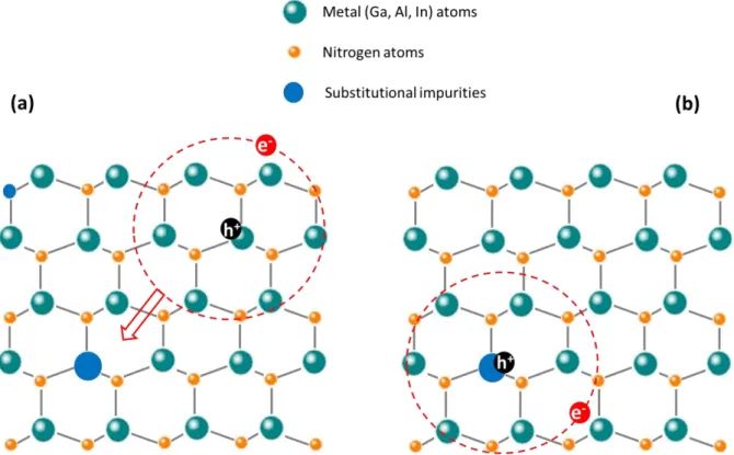
Moving within the nitride material, a given electron-hole pair, whether unbound or bound as an exciton, can also encounter structural defects or impurities (generally non-ionized) and then be trapped by or bound to the latter, as depicted for an exciton in Figure 1.2.1.2. In their vicinity, such extrinsic objects exhibit electronic configurations different from the surrounding bulk nitride material, which induces extrinsic energy levels within the bandgap of this material. In the case of substitutional atomic impurities and point defects like vacancies, interstitial or antisite defects, their associated levels can be closer to either the conduction band or the valence band, meaning that these impurities or defects respectively behave as donors or acceptors (of electrons). These levels are said to be “shallow” if they are close to either the conduction or the valence band. In contrast to shallow levels, other ones are “deep” and can be even located around the middle of the bandgap [135].
1.2 Electronic properties of III-Nitride semiconductors
28
Figure 1.2.1.2: Illustration of an exciton moving within a WZ nitride material: (a) Exciton moving freely. (b) Binding to a substitutional impurity.
Regarding excitonic transitions of extrinsic nature, excitons bound to a donor and those bound to an acceptor are noted 𝐷°𝑋 and 𝐴°𝑋, respectively. Considering 𝑋𝐴 excitons of the 𝐴-transition, their recombinations when bound to donor or acceptor can be expressed as follows:
𝐷°𝑋𝐴→ 𝐷° + 𝐸𝐷°𝑋𝐴
𝐴°𝑋𝐴→ 𝐷° + 𝐸𝐴°𝑋𝐴 (1.2.1.4)
The latter lead to emission energies 𝐸𝐷°𝑋𝐴 and 𝐸𝐴°𝑋𝐴 respectively equal to:
𝐸𝐷°𝑋𝐴 = 𝐸𝑔− 𝐸𝑋𝐴 𝑏 − 𝐸 𝐷°𝑋𝐴 𝑏 = 𝐸 𝑋𝐴− 𝐸𝐷°𝑋𝐴 𝑏 𝐸𝐴°𝑋𝐴 = 𝐸𝑔− 𝐸𝑋𝐴 𝑏 − 𝐸 𝐴°𝑋𝐴 𝑏 = 𝐸 𝑋𝐴 − 𝐸𝐴°𝑋𝐴 𝑏 (1.2.1.5)
Such emission energies related to 𝐷°𝑋 and 𝐴°𝑋 complexes are lowered by the binding energy of the exciton bound respectively to a donor and to an acceptor, i.e. 𝐸𝐷°𝑋𝑏 𝐴 and 𝐸
𝐴°𝑋𝐴
𝑏 in the case of 𝑋 𝐴. Consequently, complexes involving shallow donors exhibit emission energies close to those of free exciton recombination: the related transitions are commonly called near band edge (NBE) transitions. Typical shallow donors in nitrides are non-intentionally introduced oxygen (O) impurities substituting N (noted ON) and Si dopants substituting metal atoms, whereas residual carbon (C) impurities
substituting N (noted CN) and Mg dopants substituting metal atoms are common shallow acceptors
[128, 134]. Consequently, when performing higher Si n-doping or Mg p-doping during growth, the intensity of the emission resulting from the corresponding “shallow” 𝐷°𝑋 or 𝐴°𝑋 excitonic transition
29
will be more significant. Other NBE transitions can stem from excitons bound to extended defects such as SFs [136] or to inversion domain boundaries [111]. Other radiative and extrinsic transitions, “deeper” than those previously presented and of non-excitonic nature, can also be observed for nitrides in spectroscopy:
Donor-acceptor pair transitions (𝐷𝐴𝑃), corresponding to the carrier recombination between a neutral donor and an acceptor, and emitting at 𝐸𝐷𝐴𝑃, such as:
𝐴° + 𝐷° → 𝐴−+ 𝐷++ 𝐸𝐷𝐴𝑃 (1.2.1.6)
with
𝐸𝐷𝐴𝑃= 𝐸𝑔− 𝐸𝐷𝑏− 𝐸𝐴𝑏+ 𝑒2/(𝜀 𝑑𝐷𝐴) (1.2.1.7) where 𝑑𝐷𝐴 is the donor-acceptor distance and 𝐸𝐷𝑏 (respectively 𝐸
𝐴𝑏) is the binding energy of the electron to the donor (respectively of the hole to the acceptor). It must be noted that the donor ionization energy 𝐸𝐷𝑏 is empirically related to 𝐸
𝐷°𝑋𝑏 by Haynes’ rule [137, 138]. Such transitions are generally quite broad and asymmetric, respectively due to variation of 𝑑𝐷𝐴 and its high average magnitude making recombination less probable than for closer centers. In the case of nitrides, DAP transitions involving typical shallow donors or shallow acceptors or both are commonly observed [128, 134, 139].
Free-to-bound transitions (𝑒𝐴 or ℎ𝐷), corresponding to a recombination of an acceptor (respectively a donor) with an electron (respectively a hole) and emitting at 𝐸𝑒𝐴 (respectively 𝐸ℎ𝐷):
𝐴° + 𝑒−→ 𝐴−+ 𝐸
𝑒𝐴 (respectively 𝐷° + ℎ+→ 𝐷++ 𝐸ℎ𝐷) (1.2.1.8) where
𝐸𝑒𝐴 = 𝐸𝑔− 𝐸𝐴𝑏 (respectively 𝐸ℎ𝐷= 𝐸𝑔− 𝐸𝐷𝑏) (1.2.1.9) Due to the easier donor ionization, 𝑒𝐴 transitions are much more commonly observed than ℎ𝐷 ones in nitrides [134].
Transitions involving at least one deep level. For instance, the widely investigated broad “yellow band” emission commonly observed in GaN films or the “blue/violet” band emission in AlN layers stem from such transitions. In both cases, the origin of the latter is still under debate and being investigated. Indeed, for GaN, they are either assigned to complexes of defects/impurities comprising CN and ON [140, 141] or attributed to other complexes including
1.2 Electronic properties of III-Nitride semiconductors
30
Ga vacancies (noted VGa) and ON [142]. As for AlN, such transitions are thought to be related
to complexes formed by VAl and ON [143].
Eventually, electronic transitions can be non-radiative. Indeed, carrier recombinations do not always generate photons, especially those involving deep defects trapping carriers. Thus, crystal of low structural quality will not luminesce intensively. For instance, extended defects such as dislocations were demonstrated to behave as non-radiative recombination centers [144], which can be problematic for optoelectronic devices. Indeed, if the dislocation density is significant, the carrier diffusion length is likely to be longer than the dislocation spacing and the light emission efficiency is therefore lowered. In the perspective of enhancing such devices, intense efforts are being made to improve the III-N structure crystalline quality. In this context, nitride NWs constitute an alternative to epitaxial layers, as already mentioned. Indeed, in view of their high surface-to-volume ratio (length/diameter), they naturally grow relaxed, dislocation-free unlike their 2D counterparts and almost exempt of other defects [25, 71, 72], as supported by typical PL spectra recorded for nitride binary NWs and provided in the experimental method Subpart 2.3.1.2. The latter will consist in a direct application of the notions introduced in the present section. To conclude, Figure 1.2.1.3 sums up the main types of transitions that can be encountered in nitrides. In addition, very exhaustive reviews gathering the many transitions reported for nitrides can be found in the literature for GaN [134] and AlN [128].
31
1.2.1.3 Effect of external parameters on the band structure of bulk nitride binaries
Given that heterostructures were grown and temperature- or power-dependent optical characterization experiments were performed during this PhD, we will briefly present the effect of three external parameters in the following of this section: strain, excitation power density, and material temperature. We will detail a bit more the latter parameter.
Strain, generally resulting from heteroepitaxial growth as detailed in Subpart 1.3, induces slight modifications of nitride material lattice parameters and therefore of the metal-N bond length. Consequently, the covalence of such bond will change, leading to shifts of the bandgap and other related transitions. Figure 1.2.1.4 illustrates the linear dependence of the bandgap energy on strain for GaN and AlN.
Figure 1.2.1.4: Dependence of bandgap on in-plane strain for (a) GaN and (b) AlN under hydrostatic and biaxial stresses. Adapted from [145].
The emission energy shift of a given transition may also be caused by the variation of nitride material temperature. Indeed, the corresponding thermal expansion first induces a modification of nitride lattice parameters, resulting in a slight change in emission energy for the band gap and related transitions. Second, phonon states of higher energy get more populated when increasing temperature. Consequently, recombination of carriers coupled with such phonons usually leads to emission red-shift more significant than the one induced by the mere thermal expansion [146-148]. Regarding the bandgap transition, several models have been widely used to approach its evolution with temperature, including Varshni law [149] and Bose-Einstein model [150]. The first one is the most commonly used
1.2 Electronic properties of III-Nitride semiconductors
32
but is purely empirical, whereas the second one has physical meaning and is furthermore adapted to wide bandgap semiconductors. A third model by Pässler [151], more complex and more accurate at low temperatures, could also be used but we will stick in the following of the manuscript to the more common Varshni and Bose-Einstein laws. The corresponding expressions are given below:
𝐸𝑔𝑉.(𝑇) = 𝐸𝑔(0𝐾) − 𝛼𝑇2 𝛽 + 𝑇
(1.2.1.10) where 𝛼 and 𝛽 are the Varshni empirical coefficients.
𝐸𝑔𝐵.𝐸.(𝑇) = 𝐸𝑔(0𝐾) −
2𝛼𝐵 𝑒Θ𝐵/𝑇− 1
(1.2.1.11)
where 𝛼𝐵 is the electron-phonon coupling constant and Θ𝐵 is the characteristic Bose-Einstein temperature (related to the average phonon frequency). Typical value ranges are provided for parameters of both models in Table 1.2.1.3. The significant shift of 𝐸𝑔 with temperature over the 5-300K range is shown for GaN and AlN in Figure 1.2.1.5.
𝛼 (meV/K) 𝛽 (K) 𝛼𝐵 (meV) Θ𝐵 (K)
GaN 0.8-1.3 800-1400 80-140 300-450
AlN 1.7-2.7 1500-2600 100-400 400-700
Table 1.2.1.3: Common parameter values of Varshni and Bose-Einstein models for GaN and AlN, taken from [152] for GaN and from [153] for AlN.
Figure 1.2.1.5: Experimental evolution of bandgap with temperature for (a) GaN and (b) AlN. Taken from [154] for (a) and from [153] for (b).
33
At higher material temperatures, the phonon-carrier coupling may not only lead to the decrease in the emission energy resulting from a given transition, but may also induce:
The broadening of this emission. The linewidth can be expressed as follows:
Γ(𝑇) = Γ0+ Γ𝐴𝑇 + Γ𝐿𝑂 𝑒 ℏ𝜔𝐿𝑂 𝑘𝐵𝑇 − 1 (1.2.1.12)
where Γ𝐴 and Γ𝐿𝑂 are respectively the coupling force of acoustic and longitudinal optical (LO) phonons, and 𝜔𝐿𝑂 is the vibration frequency of LO phonons. At low temperatures, the contribution of phonons to the broadening of emission mostly stems from the acoustic phonons whereas the interaction of LO ones (also called Fröhlich coupling) gets progressively more significant when increasing temperatures [148, 152, 153].
The appearance of phonon replicas for this transition, observable in spectroscopy. Their emission is red-shifted with respect to the main transition by multiples 𝑛 of ℏ𝜔𝐿𝑂 (91 meV for GaN [13, 134] and 110 meV for AlN [128]) whereas their intensity decreases with 𝑛 [155]. For instance, due to large phonon-carrier coupling for the DAP transition (related to its polar nature), several phonon replicas are commonly observed for the latter in spectroscopy at cryogenic temperature ([128, 134, 139]).
Moreover, increasing material temperature can favor or disadvantage certain transitions defined in Subpart 1.2.1.2 with respect to other ones. Indeed, it can result in the more significant intensity quenching of a given transition compared to other ones, due to exciton dissociation, exciton unbinding from defects/impurities, or thermal escape of carriers towards other levels. For instance, free A-excitons can be dissociated at high enough temperatures, and their related intensity follows a typical Arrhenius law with an activation energy equal to its binding energy 𝐸𝑋
𝐴
𝑏 . In other words, free A-excitons exhibiting higher 𝐸𝑋𝑏𝐴 than 25 meV (𝑘
𝐵𝑇 at 300 K) are stable and can be observed at room temperature (especially for AlN in view of Table 1.2.1.2) whereas those with low 𝐸𝑋
𝐴
𝑏 are only observable at low temperatures. Another typical example is provided by the 𝐷𝐴𝑃 and 𝑒𝐴 transitions. At higher temperatures, the first ones get less observable, due to donor ionization, and red-shift, due to the decrease in the number of recombination centers (i.e. the average value of 𝑑𝐷𝐴 defined in Subpart 1.2.1.2 decreases). In contrast, 𝑒𝐴 transitions can be more easily evidenced when donor ionization is favored [134].
Eventually, excitation power density is usually set low when performing spectroscopy, in order to avoid saturating the possible energy levels related to defects, since their concentrations and associated lifetimes are finite [134]. Therefore, at higher excitation power densities, certain transitions will

![Figure 2.3.1.1: Schematic of the µ-PL setup with the CW laser. From [224].](https://thumb-eu.123doks.com/thumbv2/123doknet/12848567.367760/101.892.167.719.102.898/figure-schematic-µ-pl-setup-cw-laser.webp)