HAL Id: hal-03089577
https://hal.archives-ouvertes.fr/hal-03089577
Submitted on 28 Dec 2020
HAL is a multi-disciplinary open access
archive for the deposit and dissemination of
sci-entific research documents, whether they are
pub-lished or not. The documents may come from
teaching and research institutions in France or
abroad, or from public or private research centers.
L’archive ouverte pluridisciplinaire HAL, est
destinée au dépôt et à la diffusion de documents
scientifiques de niveau recherche, publiés ou non,
émanant des établissements d’enseignement et de
recherche français ou étrangers, des laboratoires
publics ou privés.
thin semiconductors with graphene
Etienne Lorchat, Luis Parra López, Cédric Robert, Delphine Lagarde,
Guillaume Froehlicher, Takashi Taniguchi, Kenji Watanabe, Xavier Marie,
Stéphane Berciaud
To cite this version:
Etienne Lorchat, Luis Parra López, Cédric Robert, Delphine Lagarde, Guillaume Froehlicher, et al..
Filtering the photoluminescence spectra of atomically thin semiconductors with graphene. Nature
Nanotechnology, Nature Publishing Group, 2020, 15 (4), pp.283-288. �10.1038/s41565-020-0644-2�.
�hal-03089577�
graphene
Etienne Lorchat,1, ∗ Luis E. Parra L´opez,1, ∗ C´edric Robert,2 Delphine Lagarde,2 Guillaume
Froehlicher,1 Takashi Taniguchi,3 Kenji Watanabe,3 Xavier Marie,2, 4 and St´ephane Berciaud1, 4, † 1Universit´e de Strasbourg, CNRS, Institut de Physique et Chimie des
Mat´eriaux de Strasbourg (IPCMS), UMR 7504, F-67000 Strasbourg, France
2Universit´e de Toulouse, INSA-CNRS-UPS, LPCNO,
135 Avenue de Rangueil, 31077, Toulouse, France
3
National Institute for Materials Science, Tsukuba, Ibaraki 305-0044, Japan
4
Institut Universitaire de France, 1 rue Descartes, 75231 Paris cedex 05, France Atomically thin semiconductors made from transition metal dichalcogenides (TMDs) are model systems for investigations of strong light-matter interactions and applications in nanophotonics, opto-electronics and valley-tronics. However, the photoluminescence spectra of TMD monolayers display a large number of features that are particularly challenging to decipher. On a practical level, monochromatic TMD-based emitters would be beneficial for low-dimensional devices but this challenge is yet to be resolved. Here, we show that graphene, directly stacked onto TMD mono-layers enables single and narrow-line photoluminescence arising solely from TMD neutral excitons. This filtering effect stems from complete neutralization of the TMD by graphene combined with selective non-radiative transfer of long-lived excitonic species to graphene. Our approach is applied to four tungsten and molybdenum-based TMDs and establishes TMD/graphene heterostructures as a unique set of opto-electronic building blocks, suitable for electroluminescent systems emitting visible and near-infrared photons at near THz rate with linewidths approaching the lifetime limit.
TMD monolayers (thereafter simply denoted TMD), such as MoS2, MoSe2, WS2, WSe2 are direct-bandgap
semiconductors [1, 2], featuring short Bohr radii, large exciton binding energy of hundreds of meV [3, 4] and picosecond excitonic radiative lifetimes at low temper-ature [5–7], all arising from their strong 2D Coulomb interactions, reduced dielectric screening and large effec-tive masses [3, 4]. Since the first investigations of light emission from TMDs, it has been clear that their low-temperature spectra is composed of at least two promi-nent features, stemming from bright neutral excitons (X0) and charged excitons (trions, X?) [8–10] endowed
with a binding energy of typically 20 to 40 meV rela-tive to X0. Among the vast family of TMDs, one may distinguish between so-called dark and bright materi-als [11]. In the case of Tungsten-based TMDs, a spin-dark state lies lower than X0. Conversely, in
Molybde-num based-TMDs, X0 lies below (MoSe
2) or very near
(MoS2) the spin-dark state, resulting in brighter
emis-sion at low temperature. As a result, X0 and X? emis-sion dominate the PL spectrum of Mo-based TMDs [9], whereas the emission spectra of W-based TMDs dis-play a complex series of lines stemming from X0,
bi-excitons (XX0)[12–15], charged excitonic states (includ-ing X? [10, 16] and charged biexcitons (XX?) [12–15]), spin-dark excitons [17–19], defect-induced emission and exciton-phonon sidebands [20, 21].
Considerable progress has been made to determin-istically observe intrinsic TMD emission features. In particular, encapsulation of TMDs in hexagonal boron
∗These authors contributed equally to this study
†stephane.berciaud@ipcms.unistra.fr
nitride (BN) films results in narrower neutral exciton linewidth [22, 23], approaching the radiative limit [7, 24, 25], without however, getting rid of the other emission features mentioned above. Even in electrostatically gated devices tuned near the charge neutrality point, sizeable emission sidebands remain observable at energies close to the X? feature, suggesting residual charge
inhomo-geneity [9, 10] or intrinsic contributions from longer-lived exciton-phonon replicas [20, 21].
The complex emission spectra of TMD stimulate lively scientific debates. Conversely, obtaining atomically-thin semiconductors with single, narrow emission lines re-mains an important challenge in the field. An appeal-ing solution could consist in interfacappeal-ing a TMD mono-layer with graphene. Indeed, the semi-metallic char-acter of graphene and its highly symmetric electronic structure [26], with its Dirac point lying within the bandgap of Mo- and W- based TMD [27], makes it an ideal electron and hole acceptor, through static charge transfer [28, 29]. Unfortunately, at room temperature, the effective X0 lifetime is in the ns range [5, 6, 29]
and interlayer coupling between TMDs and graphene re-sults in significant PL quenching [29–31] due to picosec-ond energy transfer mediated by either charge tunneling (Dexter-type) or longer-range dipole-dipole interaction (F¨orster-type) [29, 32, 33]. However, a much more fa-vorable situation may occur at lower temperatures (typ-ically, below 100 K), where the radiative lifetime of X0 drastically shortens [5, 6] and becomes of the same or-der of magnitude as the theoretically estimated energy transfer time [32].
In this work, we demonstrate that W- and Mo-based TMDs coupled to a graphene monolayer exhibit only one single and narrow emission line that is assigned to
0
1
1.6
1.7
1.8
1.9
2.0
2.1
0
1
PL In
ten
si
ty
(a
rb
. u
ni
ts
)
WSe2 MoS2 WS2 /4.9 /3.4 /6.0 /3.4*
*
*
*
X0 X* X* X0 X0 X0 X* X* MoSe2Energy (eV)
WSe2/Gr MoS2/Gr WS2/Gr MoSe2/Gr0
1
1.6
1.7
1.8
1.9
2.0
2.1
0
1
PL In
ten
sity (a
rb
. u
nits)
WSe2 MoS2 WS2 /3.6 /9.1 /5.9 /86*
*
*
*
MoSe2Energy (eV)
WSe2/Gr MoS2/Gr WS2/Gr MoSe2/Gr BN BN TMD BN BN TMD GrFIG. 1. Graphene as a versatile emission filter. Bright, single, and narrow-line photoluminescence (PL) spectra in TMD/graphene heterostructures are shown in the lower panel. The PL spectra of neighboring BN-capped TMD regions are shown for comparison in the upper panel. A sketch of the van der Waals heterostructure is shown in each panel. All spectra are normalized to unity relative to their most intense feature. The scaling factors indicated for each material allow direct comparison between the PL intensities in BN-capped TMD and BN-capped TMD/graphene. The bright neutral exciton (X0)
lines in bare TMD are indicated by asterisks. All measurements were performed at temperatures below 20 K, in the linear regime with continuous wave laser excitation at 2.33 eV (MoSe2, MoS2, WS2) or 1.96 eV (WSe2).
X0 radiative recombination, indicating complete neu-trality. The short-lived X0 states are minimally
af-fected by non-radiative transfer to graphene and sub-sequent PL quenching, in stark contrast with longer-lived excitonic species, which are massively quenched. Graphene has been recognised as a partner material of choice to improve the opto-electronic response of TMDs [34], whereas TMDs hold promise to improve spin transport in graphene [35, 36]. Our results now estab-lish TMD/graphene heterostructures as an outstanding light-emitting system readily interfaced with a quasi-transparent conductive channel.
Bright, single-line emission in TMD/graphene heterostructures
Figure 1 shows the PL spectra of van der Waals het-erostructures made from monolayers of MoS2, MoSe2,
WS2 and WSe2 stacked onto graphene monolayers and
encapsulated in BN (lower panel). These spectra are compared to those of neighbouring BN-capped TMD re-gions (upper panel). All TMD/graphene spectra dis-play one single and narrow Lorentzian emission line, with a full width at half maximum (FWHM) of typ-ically 5 meV, suggesting minimal dephasing and dis-order (see supplementary Section 1 for the fitting pa-rameters and Section 2 for MoSe2/graphene samples
with PL linewidths approaching the lieftime limit). The TMD references also display narrow emission features as-signed to X0 (see asterisks in Fig. 1, upper panel), but
the latter are accompanied with the lower energy emis-sion lines introduced above [3, 16, 21, 22] (see supple-mentary Section 3 for their assignments). The sharp PL lines in TMD/graphene are slightly redshifted (by ∼ 10 meV) with respect to X0 in the TMD references.
By measuring the temperature dependent PL spectra and the differential reflectance (DR) spectra of TMD and TMD/graphene, we can unambiguously assign these sin-gle lines to X0 (see Fig. 2 and supplementary Section 4). Therefore, we conclude (i) that no X? emission is
mea-sured in TMD/graphene and (ii) that the X0 redshift in
TMD/graphene arises from dielectric screening [29, 37]. Crucially, we note that PL quenching of the X0 line is
moderate, systematically of less than one order of mag-nitude in all samples under study (see Fig. 1 and sup-plementary Section 1). The difference between PL from TMD and TMD/graphene heterostructures is particu-larly striking in the case of tungsten-based TMDs. In these dark materials, hot luminescence from X0 is quite inefficient and lower lying emission lines dominate the PL spectra, especially in WS2, (see Fig. 1 and
supplemen-tary Section 3). As discussed below, all these features are much longer lived than X0 in TMD [6, 17, 38, 39]
(a) 5µm Gr MoSe2 0 5 10 15 0 5 10 0 5 10 15 (c) (d) 5µm (b) 1 2 1.60 1.65 10-2 10-1 100 1 3 1.55 1.60 1.65 0 1 1.55 1.60 1.65 0 1 (f) (e) MoSe 2/Gr Δ R/R MoSe2 X0 X* X0 Energy (eV) PL Intensity (a.u.) Energy (eV) x5 �X0 (meV) IX0 (arb.units) IX* (arb.units)
FIG. 2. Neutralizing an atomically thin semiconductor with graphene. (a) Optical image of a BN-capped MoSe2/graphene sample deposited onto a SiO2 coverslip. Maps of the neutral exciton (X0) emission FWHM (ΓX0) (b) and integrated intensity IX0 (c). (d) Map of the trion (X?) integrated PL intensity (IX0). No X? emission is observed over the whole MoSe2/graphene area. Differential reflectance spectra ∆R/R and PL spectra of (e) MoSe2 and (f) MoSe2/graphene,
taken at the spots indicated in white and red on (b-d), respectively. The inset in (f) shows the PL spectrum of MoSe2/graphene
on a semi-logarithmic scale. The data are recorded at a temperature of 4 K, in the linear regime using continuous wave laser excitation at 2.33 eV.
and are thus literally washed out in the emission spec-tra of TMD/graphene heterostructures due to fast non-radiative transfer to graphene.
Complete TMD neutralization
We now focus on the case of MoSe2/graphene
het-erostructures, with PL mapping, as well as typical DR and PL spectra shown in Fig. 2 for a BN-capped sam-ple deposited onto a glass coverslip. The PL spectrum of BN-capped MoSe2 is composed of two lines with
sim-ilar intensities, shifted by 28 meV. The high and low-energy line are assigned to X0and X?PL [9], respectively. An X? absorption feature emerges on the DR spectrum, with an amplitude considerably smaller than that of the X0 DR feature (Fig. 2e). In contrast, the BN-capped
MoSe2/graphene region of the sample displays only X0
absorption and emission features. As shown in Fig. 2b-d, these observations can be consistently made over the whole (> 40 µm2) area of a coupled MoSe
2/graphene
re-gion. This is an important point, since TMD-based van der Waals heterostructures are known to be spatially in-homogeneous and hence, the observation of “trion-free” spectra might be accidental. In return, the absence of X? emission can be exploited as a reliable probe of the
coupling between TMD and graphene.
We assign the absence of X? absorption and emission
features in TMD/graphene to the transfer of all the na-tive dopants in the TMD (either electrons or holes, with a typical density on the order of 1011− 1012 cm−2) to
graphene. Such static charge transfer leads to a slight increase of the Fermi level of graphene (typically by less than 100 meV) and to the observation of intrinsic
absorp-tion and emission. Alternate scenarii, involving resid-ual doping in the TMD but massive quenching of X? formation and/or radiative recombination can safely be ruled out (see supplementary Section 5.1). TMD neu-tralization is corroborated by room temperature Raman scattering [29] and PL measurements (see supplementary Section 5.2).
Photostability and dielectric screening
To further establish the benefits of coupling TMD to graphene, we show, in Fig. 3, the PL spectra of the BN-capped MoSe2/graphene introduced in Fig. 2 recorded
under continuous wave (cw) photon fluxes (hereafter de-noted Φph) at 2.33 eV, spanning more than five orders of
magnitude, from 1×1018cm−2 s−1to 3×1023cm−2 s−1,
i.e., ≈ 1 mW/µm2. Assuming an absorptance of ∼ 10 %
at 2.33 eV [40] and an excitonic lifetime of 2 ps in BN-capped MoSe2/graphene (see Fig. 4,5), we may estimate
injected hot exciton densities ranging from 2 × 105cm−2 up to 6 × 1010 cm−2. The X0 PL intensity scales quasi-linearly with Φph. We note, however, the emergence
of two faint PL features. The first one is asymmetric, blueshifted by about 120 meV from X0 and its
inten-sity scales linearly with Φph. We assign this feature to
hot luminescence from the neutral excited X02s excitons
(at ∆1s−2s = 110 meV) and X03s excitons (at ∆1s−3s =
127 meV). The exciton binding energy is Eb= 231 meV
in BN-capped MoSe2, with ∆1s−2s≈ 168 meV.
Assum-ing for simplicity that Ebscales proportionally to ∆1s−2s,
we estimate that the presence of a graphene layer reduces Ebdown to ≈ 148 meV (see supplementary Section 6).
101810191020102110221023 10-2 10-1 100 101 102 103 104 1.6 1.7 1.8 1.9 X0 3s (c) X0 2s X* Energy (eV) P L inten s it y ( a rb . u n it s ) 1.6 1.7 1.8 1.9 0 1 X* P L I n te n s it y ( a rb .u n it s ) Energy (eV) X0 0 1 2 20 30 EX 0 E X* ( meV) (a) FPh (x10 23cm-2s-1) (b) FPh (cm-2s-1) X0 b = 1.0 b = 1.1 X0 X0 2s + X 0 3s X* P L I n te n s it y ( a rb .u n it s ) b = 2.0 1.7 1.8 1 2 3 X0 2s X0 3s x103 FPh ( x 10 21 cm -2s -1) 10-3 102
FIG. 3. Laser power dependent photoluminescence in BN-capped TMD/graphene at 4 K. (a) Semi-logarithmic cascade plot of the PL spectra of the BN-capped MoSe2/graphene sample shown in Fig. 1,2, recorded under cw excitation at
2.33 eV with increasing photon fluxes Φph. The spectra are normalized by Φph and by the integration time and are vertically
shifted for clarity. (b) Dependence of the integrated intensity of the neutral 1s exciton (X0 brown), sum of the first and second
excited neutral excitons X0
2s and X03s (orange) and photoinduced trion (X?, green). The solid lines are fits based on a power
law and the critical exponents β are indicated. (c) PL spectrum recorded at Φph= 3 × 1023cm−2s−1showing the X0 and X?
features on a linear scale. The X02sand X03sfeatures are shown in the lower inset, where the red line is a double-Lorentzian fit
to the data, with the X0
2sand X03sfeatures individually shown with dashed grey lines. The upper inset in (c) shows the energy
difference between X0and X?as a function of Φph.
a few meV less than the X? line in MoSe
2 (see Fig. 2c)
and its intensity rises quadratically with Φph. Therefore,
this feature could tentatively be assigned to a biexciton (XX0). However, XX0 have recently been observed in MoSe2 [41] and WSe2 [12–15] monolayers and display
binding energies of . 20 meV, significantly lower than the value observed here in a system that undergoes more screening due to the presence of graphene. Thus, the lower energy feature is tentatively assigned to emission from photocreated trions with a slightly reduced binding energy. As previously reported in other low-dimensional materials (e.g.; carbon nanotubes [42]), at sufficiently large exciton densities, bimolecular exciton-exciton anni-hilation (EEA [43]) can create free carriers. Subsequent photon absorption leads to X? formation and emission. In this scenario, a quadratic scaling with Φphis expected.
Noteworthy, X0emission remains more than one order of
magnitude brighter than X? emission at the highest Φ ph
employed here, which justifies why we do not observe a sub-linear rise of the X0 PL intensity due to EEA. The data in Fig. 3 also reveals the outstanding photostability of TMD/graphene systems that can sustain photon fluxes above typical PL non-linearity and damage thresholds in bare TMD [44], without significant photo-induced heat-ing (see supplementary Sections 5 and 7).
Exciton dynamics and exciton transfer time Let us finally consider exciton dynamics in TMD/graphene. Fig. 4 compares the time-resolved PL (TRPL) of MoSe2 and MoSe2/graphene, recorded
at 14 K on another sample deposited on SiO2 and
excited below the X0
2s state. As shown in Fig. 4a, the
filtering effect evidenced in BN-capped TMD/graphene (Fig. 1) also appears prominently samples supported by a rougher SiO2 substrate (see also supplementary
Section 2). A three-level system [7] considering hot excitons Xh, such as finite momentum 1s and possibly 2s excitons, formed shortly after laser excitation [45], X0(i.e., cold 1s excitons with center of mass momentum
within the light cone) and the ground state is shown in the inset of Fig. 4a. As the PL rise time lies below our time resolution for all measurements on this sample, the TRPL traces in Fig. 4 are simply fit by the convolution of the instrument response function (IRF) with an exponential decay. In keeping with previous reports, the X0 exciton lifetime (τ
X0) is only ≈ 2.3 ps in bare
MoSe2, and can be assigned to the radiative lifetime
τXrad0 [6], whereas X
? display a much longer lifetime
τX?= 30 ps. Remarkably, within experimental accuracy,
τX0 has identical values in MoSe2/graphene and in the
neighbouring MoSe2region. This striking result suggests
that τG0, the non-radiative transfer time of cold excitons (X0) to graphene, is longer than 2 ps. Let us note, that τrad
X0 scales as E
−2
b and is thus expected to be longer in
MoSe2/graphene than in the nearby MoSe2 reference.
Hence, observing similar τX0 in Fig. 4b,c may be
coin-cidental and result from the compensation between the increase of τXrad0 in MoSe2/graphene and non-radiative
transfer of X0 to graphene with an estimated timescale
τ0
G ∼ 5 ps (see supplementary Section 8.1). As a result,
the X0 emission yield (defined here as the number of
emitted photons divided by the number of cold X0) that
is near unity in the bare MoSe2 monolayer [7] remains
0 20 40 10-2 10-1 100 1.60 1.65 0 1 2 3 0 20 40 10-2 10-1 100 0 50 100 10-2 10-1 100 1.60 1.65 10-2 10-1 100 tX0 = 2.3 ps PL in te n sity (a. u .) Time (ps) IRF (c) X0 X0 X* MoSe2/Gr MoSe2 PL in te n sity (a. u .) Energy (eV) tX0 = 2.3 ps PL in te n sity (a. u .) Time (ps) IRF MoSe2 SiO2 Gr MoSe2 SiO2 MoSe2 SiO2 PL in te n sity (a. u .) Time (ps) IRF tX* = 30 ps (b) (d) (a) L X0 X0 X*
FIG. 4. Low-temperature exciton dynamics. (a) PL spectra of bare MoSe2 monolayer (blue) and of a MoSe2/graphene
heterostructure (red, thicker line), both deposited onto a SiO2substrate (see sample sketches in (b)-(d). The right inset shows
the data on a semi-logarithmic scale. The grey-shaded area highlights a low-energy PL tail from localised (L) states in bare-MoSe2 that is massively quenched in MoSe2/graphene. A three-level system is shown on the left inset. The blue wavy arrow
indicates the exciting laser pump pulse that generates a population of hot excitons (Xh). The latter relax with a lifetime τrel
to form cold excitons (X0), from which radiative recombination occurs with a lifetime τXrad0. The presence of graphene induces non-radiative decay of Xh and X0 with timescales τGh and τ
0
G, respectively. A similar sketch may be drawn for X ?
and other excitonic sates. Time-resolved PL of the neutral exciton feature (X0) in MoSe2/graphene (b), and in bare MoSe2 (c). The
longer-lived tail in the bare MoSe2PL decay is attributed to exciton localisation. (d) TRPL of the trion feature (X?) in MoSe2.
All data were recorded at 14 K in the linear regime under excitation with ps laser pulses at 1.76 eV. The thin solid lines are mono-exponential fits to the data after convolution with the instrument response function (IRF, grey area). The extracted X0 and X?lifetimes (τ
X0 and τX?, respectively) are indicated.
Section 8.2).
Still, while the integrated PL intensity from X0 in MoSe2/graphene on SiO2 is nearly twice that of a
close-lying MoSe2 reference (see Fig. 4a), the total PL
inten-sity from MoSe2remains ≈ 4.5 times larger than that of
MoSe2/graphene. Following generation of Xh, one may
form X0, X?and localised excitons (e.g., near defects) in bare MoSe2. Localised excitons contribute a low-energy
tail to the PL spectra, as shown in Fig. 4a (shaded area under the blue trace). Conversely, only X0and localised
excitons can be formed in neutral graphene/MoSe2/SiO2,
which is consitent with the observed enhancement of X0
emission. Since localised excitons have long lifetimes [38], their emission is quenched by graphene, as evidenced in Fig. 4a (red trace). The sizeable quenching of the total PL intensity can tentatively be assigned to fast trans-fer of Xh to graphene on a time scale τh
G (see inset in
Fig. 4a) that is shorter than τrel, the relaxation time of
Xh down to the light cone. This scenario is consistent with the fact that the F¨orster-type energy transfer time
of TMD excitons to graphene is expected to be maximal for zero momentum excitons (i.e., here X0) and to de-crease with exciton momentum [32, 33]. All in all, our results strongly suggest that graphene open up efficient non-radiative decay pathways that moderately quench X0
radiative recombination but instead significantly inhibit X0 formation. Along these lines, we expect that X0 for-mation should be more efficiently inhibited in BN-capped samples, where τrelis much longer than in SiO2supported
samples and can be experimentally resolved [7]. Efficient hot exciton transfer to graphene In Fig. 5, we investigate exciton dynamics the BN-capped sample discussed in Fig. 1-3, following pulsed optical excitation slightly below the X0
2s exciton energy.
Importantly, this sample is deposited on a glass cover-slip and therefore immune from the cavity effects dis-cussed in ref. [7]. As introduced in Fig. 1-3, X0 PL is quenched in MoSe2/graphene, in contrast with the case
enhance-0 20 40 10-2 10-1 100 1.62 1.64 1.66 0 1 0 20 40 10-2 10-1 100 0 50 100 10-2 10-1 100 PL in te n sity (a. u .) Time (ps) PL in te n sity (a. u .) Energy (eV) /7.3 X* X0 X0 MoSe2 MoSe2/Gr (a) MoSe2 t'rel~ 1.5ps tX0= 2.2ps PL in te n sity (a. u .) Time (ps) trel= 5.0ps tX0= 2.4ps MoSe2 (b) (c) (d) Gr BN BN IRF PL in te n sity (a. u .) Time (ps) IRF trel= 5.1ps tX*= 62ps IRF BN MoSe2
FIG. 5. Evidence for hot exciton transfer to graphene. (a) PL spectra of BN-capped MoSe2 monolayer (blue) and a
BN-capped MoSe2/graphene heterostructure (red), both deposited onto a SiO2 coverslip (see sample sketches in (b)-(d)). The
PL spectrum of BN-capped MoSe2 is scaled down by a factor 7.3 for a clearer comparison. Time-resolved PL of the neutral
exciton feature (X0) in BN-capped MoSe
2/graphene (b), and in BN-capped MoSe2 (c). The longer lived tail in the MoSe2 PL
decay is attributed to exciton localisation. (d) TRPL of the trion feature (X?) in MoSe2. All data were recorded at 7 K in
the linear regime under excitation with ps laser pulses at 1.73 eV. The thin solid lines are fits to the data using the three-level model shown in the inset of Fig. 4a, after convolution with the instrument response function (IRF, grey area). The extracted hot exciton relaxation times (τrel0 in (b), τrel in (c)) as well as the X0 and X? decay times (τX0 and τX?, respectively) are indicated.
ment is observed (Fig. 4a). This difference readily sug-gests that X0 formation is more efficiently quenched in BN-capped TMD/graphene. The TRPL traces are fit by solving the rate equations associated with the three-level system introduced in Fig. 4a, with two character-istic times for Xh relaxation towards X0 (or X?)
for-mation and X0 (or X?) decay, respectively. The short and long times correspond to the rise and decay times in the TRPL measurement, respectively [7]. Fig. 5b,c reveals that the PL rise time (∼ 1.5 ps) is too close to our resolution limit to be accurately resolved in BN-capped MoSe2/graphene and is 2.4 ps in the BN-capped
MoSe2 reference. The PL decay times are ≈ 2.2 ps in
MoSe2/graphene and ≈ 5 ps in the MoSe2 reference
re-gion, respectively. Interestingly, the ≈ 5.1 ps PL rise time of the long-lived X? feature (τ
X? = 62 ps) in
BN-capped MoSe2 is closely matching the X0 decay time.
We therefore assign this ≈ 5 ps time to τrel, the
relax-ation time of Xh down to the X? and X0 states in BN-capped MoSe2. Hot exciton transfer results in a
short-ened Xh relaxation time τ0
rel . 1.5 ps in BN-capped
MoSe2/graphene. Finally, the X0 lifetimes τX0 in
BN-capped MoSe2 and MoSe2/graphene are assigned to the
rise and decay time of their respective TRPL traces and are nearly identical (≈ 2.4 ps and ≈ 2.2 ps, respectively). With these values, following the same reasoning as for the SiO2-supported MoSe2/graphene sample discussed in
Fig. 4, we can estimate that the X0emission yield is also
near 50 % (see supplementary Section 8.2), demonstrat-ing that non-radiative X0 transfer has similar efficien-cies in BN-capped and SiO2-supported MoSe2/graphene
heterostructures. We conclude that a significant part of X0 PL quenching is due to efficient non-radiative
trans-fer of Xh enabled by graphene and that X0 PL
quench-ing is more efficient in BN-capped Mose2/graphene than
SiO2/MoSe2/graphene due to slower Xh relaxation (or
equivalently X0formation) in BN-capped MoSe 2.
Conclusions and outlook
In closing, we have shown that graphene neutralizes atomically-thin TMDs, leading to the absence of light emission from charged excitonic species. Graphene also enables picosecond non-radiative transfer of TMD exci-tonic species. Starting from a given initial Xh density, transfer of Xh to graphene will reduce the maximum achievable density of X0 and of other longer lived
neu-tral excitonic compounds. The latter will be strongly quenched by graphene, whereas the former will be min-imally affected owing to their picosecond radiative life-time. As a result, X0 exclusively contribute to the PL
spectra of TMD/graphene heterostructures. The mea-sured X0 PL intensity is largely determined by the com-petition between X0 formation and non-radiative Xh transfer to graphene rather than by the trade-off between radiative X0recombination and non-radiative X0transfer
to graphene.
Graphene is here introduced as narrow-line filter that is naturally tuned to a broad range of emitted photon energies spanning the mid-infrared to the ultraviolet re-gions. Our two-dimensional design naturally outperforms alternate solutions based on spectrally narrow interfer-ence filter that are considerably bulkier and lack tunabil-ity (see supplementary Section 9). Going further, high-speed (up to ∼ 1THz), photonic and opto-electronic de-vices with one single bright and nearly lifetime-limited emission line (see supplementary Section 2) can be envi-sioned using TMD/graphene heterostructures. Such de-vices may also benefit from the excellent electrical con-tact, photodetection [34, 46], electron and spin trans-port [35, 36] capabilities offered by TMD/graphene het-erostructures. One may also foresee progress in cav-ity quantum electrodynamics [47], chiral optics [48] and opto-valleytronics [49] by jointly exploiting the simple emission spectra of TMD/graphene heterostructures and their record-high degrees of valley coherence and valley polarization of up to 60 % and 50 %, respectively [50].
Acknowledgements
The authors thank D. Basko, T. Galvani, L. Wirtz, G. Schull, S. Azzini, T. Chervy, C. Genet, M.A. Sem-ina and M.M. Glazov for fruitful discussions. We are grateful to H. Majjad and M. Rastei for help with AFM measurements, to M. Romeo, F. Chevrier, M. Acosta, A. Boulard and the StNano clean room staff for techni-cal support. We acknowledge financial support from the Agence Nationale de la Recherche (under grants H2DH ANR-15-CE24-0016, 2POEM ANR-18-ERC1-0009, D-vdW-Spin, VallEx, and MagicValley), from the LabEx
NIE (Under Grant ANR-11-LABX-0058-NIE) and from the EUR NanoX (under grant VWspin and MILO).
Competing interests
The authors declare no competing interests. Author contributions
S.B. conceived and lead the project, with C.R., D.L. and X.M. supervising the time-resolved PL measure-ments. E.L. and L.E.P.L. fabricated the samples. E.L., L.E.P.L., C.R., D.L. and S.B. carried out the measure-ments. E.L., L.E.P.L. and S.B. analysed the data with input from G.F., C.R., D.L. and X.M. T.T. and K.W. provided high-quality hexagonal BN crystals. S.B. wrote the manuscript with input from X.M., C.R., E.L. and L.E.P.L.
Methods
Our model system is a van der Waals heterostructure formed by stacking a monolayer of graphene onto a TMD monolayer using standard methods as in ref. [51, 52]. In this work, we have investigated MoSe2, MoS2, WSe2and
WS2-based heterostructures encapsulated in hexagonal
boron nitride (BN, see Fig. 1- 3 and Fig. 5) or directly deposited on SiO2substrates (Fig. 4). All materials were
mechanically exfoliated from bulk crystals. Graphene and TMD monolayers were unambiguously identified us-ing room-temperature Raman and PL spectroscopies, re-spectively. Our samples were investigated at variable temperature (4 K – 300 K) by means of micro-PL and dif-ferential reflectance (DR) spectroscopy using home-built setups. Time-resolved PL measurements were performed on MoSe2-based samples, using a Ti:Sa oscillator
deliv-ering ≈ 2 ps pulses with a repetition rate of 80 MHz and a synchro-scan streak camera with a temporal resolution of ≈ 1.5 ps. All comparisons between results obtained on TMD and on TMD/graphene are based on measure-ments performed in the same experimental conditions on a same TMD flake partially covered with graphene (see for example Fig. 2).
[1] Kin Fai Mak, Changgu Lee, James Hone, Jie Shan, and Tony F. Heinz, “Atomically Thin MoS2: A New
Direct-Gap Semiconductor,” Phys. Rev. Lett. 105, 136805 (2010).
[2] Andrea Splendiani, Liang Sun, Yuanbo Zhang, Tianshu Li, Jonghwan Kim, Chi-Yung Chim, Giulia Galli, and Feng Wang, “Emerging Photoluminescence in Monolayer MoS2,” Nano Lett. 10, 1271–1275 (2010).
[3] Gang Wang, Alexey Chernikov, Mikhail M. Glazov, Tony F. Heinz, Xavier Marie, Thierry Amand, and Bern-hard Urbaszek, “Colloquium: Excitons in atomically thin transition metal dichalcogenides,” Rev. Mod. Phys. 90,
021001 (2018).
[4] M. Goryca, J. Li, A. V. Stier, T. Taniguchi, K. Watanabe, E. Courtade, S. Shree, C. Robert, B. Urbaszek, X. Marie, and S. A. Crooker, “Revealing exciton masses and dielec-tric properties of monolayer semiconductors with high magnetic fields,” Nat. Commun. 10, 4172 (2019). [5] Maurizia Palummo, Marco Bernardi, and
Jef-frey C Grossman, “Exciton radiative lifetimes in two-dimensional transition metal dichalcogenides,” Nano Lett. 15, 2794–2800 (2015).
[6] C. Robert, D. Lagarde, F. Cadiz, G. Wang, B. Lassagne, T. Amand, A. Balocchi, P. Renucci, S. Tongay, B.
Ur-baszek, and X. Marie, “Exciton radiative lifetime in transition metal dichalcogenide monolayers,” Phys. Rev. B 93, 205423 (2016).
[7] H. H. Fang, B. Han, C. Robert, M. A. Semina, D. Lagarde, E. Courtade, T. Taniguchi, K. Watanabe, T. Amand, B. Urbaszek, M. M. Glazov, and X. Marie, “Control of the exciton radiative lifetime in van der waals heterostructures,” Phys. Rev. Lett. 123, 067401 (2019). [8] Kin Fai Mak, Keliang He, Changgu Lee, Gwan Hyoung
Lee, James Hone, Tony F Heinz, and Jie Shan, “Tightly bound trions in monolayer mos2,” Nat. Mater. 12, 207– 211 (2013).
[9] Jason S Ross, Sanfeng Wu, Hongyi Yu, Nirmal J Ghimire, Aaron M Jones, Grant Aivazian, Jiaqiang Yan, David G Mandrus, Di Xiao, Wang Yao, et al., “Electrical control of neutral and charged excitons in a monolayer semicon-ductor,” Nat. Commun. 4, 1474 (2013).
[10] E. Courtade, M. Semina, M. Manca, M. M. Glazov, C. Robert, F. Cadiz, G. Wang, T. Taniguchi, K. Watan-abe, M. Pierre, W. Escoffier, E. L. Ivchenko, P. Renucci, X. Marie, T. Amand, and B. Urbaszek, “Charged exci-tons in monolayer WSe2: Experiment and theory,” Phys.
Rev. B 96, 085302 (2017).
[11] J. P. Echeverry, B. Urbaszek, T. Amand, X. Marie, and I. C. Gerber, “Splitting between bright and dark excitons in transition metal dichalcogenide monolayers,” Phys. Rev. B 93, 121107 (2016).
[12] Matteo Barbone, Alejandro R-P Montblanch, Dhiren M Kara, Carmen Palacios-Berraquero, Alisson R Cadore, Domenico De Fazio, Benjamin Pingault, Elaheh Mostaani, Han Li, Bin Chen, et al., “Charge-tuneable biexciton complexes in monolayer WSe2,” Nat. Commun.
9, 3721 (2018).
[13] Ziliang Ye, Lutz Waldecker, Eric Yue Ma, Daniel Rhodes, Abhinandan Antony, Bumho Kim, Xiao-Xiao Zhang, Minda Deng, Yuxuan Jiang, Zhengguang Lu, et al., “Ef-ficient generation of neutral and charged biexcitons in encapsulated wse 2 monolayers,” Nat. Commun. 9, 3718 (2018).
[14] Matthias Paur, Aday J. Molina-Mendoza, Rudolf Brats-chitsch, Kenji Watanabe, Takashi Taniguchi, and Thomas Mueller, “Electroluminescence from multi-particle exciton complexes in transition metal dichalco-genide semiconductors,” Nat. Commun. 10, 1709 (2019). [15] Zhipeng Li, Tianmeng Wang, Zhengguang Lu, Chen-hao Jin, Yanwen Chen, Yuze Meng, Zhen Lian, Takashi Taniguchi, Kenji Watanabe, Shengbai Zhang, Dmitry Smirnov, and Su-Fei Shi, “Revealing the biexciton and trion-exciton complexes in bn encapsulatedWSe2,” Nat.
Commun. 9, 3719 (2018).
[16] D Vaclavkova, J Wyzula, K Nogajewski, M Bartos, A O Slobodeniuk, C Faugeras, M Potemski, and M R Molas, “Singlet and triplet trions in WS2 monolayer encapsu-lated in hexagonal boron nitride,” Nanotechnology 29, 325705 (2018).
[17] C. Robert, T. Amand, F. Cadiz, D. Lagarde, E. Cour-tade, M. Manca, T. Taniguchi, K. Watanabe, B. Ur-baszek, and X. Marie, “Fine structure and lifetime of dark excitons in transition metal dichalcogenide mono-layers,” Phys. Rev. B 96, 155423 (2017).
[18] You Zhou, Giovanni Scuri, Dominik S Wild, Alexander A High, Alan Dibos, Luis A Jauregui, Chi Shu, Kristiaan De Greve, Kateryna Pistunova, Andrew Y Joe, et al., “Probing dark excitons in atomically thin
semiconduc-tors via near-field coupling to surface plasmon polari-tons,” Nat. Nanotechnol. 12, 856 (2017).
[19] Xiao-Xiao Zhang, Ting Cao, Zhengguang Lu, Yu-Chuan Lin, Fan Zhang, Ying Wang, Zhiqiang Li, James C Hone, Joshua A Robinson, Dmitry Smirnov, et al., “Magnetic brightening and control of dark excitons in monolayer WSe2,” Nat. Nanotechnol. 12, 883 (2017).
[20] Jessica Lindlau, Malte Selig, Andre Neumann, L´eo Colombier, Jonathan F¨orste, Victor Funk, Michael F¨org, Jonghwan Kim, Gunnar Bergh¨auser, Takashi Taniguchi, et al., “The role of momentum-dark excitons in the el-ementary optical response of bilayer wse 2,” Nat. Com-mun. 9, 2586 (2018).
[21] Erfu Liu, Jeremiah van Baren, Takashi Taniguchi, Kenji Watanabe, Yia-Chung Chang, and Chun Hung Lui, “Valley-selective chiral phonon replicas of dark excitons and trions in monolayer WSe2,” Phys. Rev. Research 1,
032007 (2019).
[22] F. Cadiz, E. Courtade, C. Robert, G. Wang, Y. Shen, H. Cai, T. Taniguchi, K. Watanabe, H. Carrere, D. La-garde, M. Manca, T. Amand, P. Renucci, S. Tongay, X. Marie, and B. Urbaszek, “Excitonic linewidth ap-proaching the homogeneous limit in MoS2-based van der
waals heterostructures,” Phys. Rev. X 7, 021026 (2017). [23] Obafunso A Ajayi, Jenny V Ardelean, Gabriella D Shep-ard, Jue Wang, Abhinandan Antony, Takeshi Taniguchi, Kenji Watanabe, Tony F Heinz, Stefan Strauf, X-Y Zhu, and James C Hone, “Approaching the intrinsic photolu-minescence linewidth in transition metal dichalcogenide monolayers,” 2D Materials 4, 031011 (2017).
[24] Giovanni Scuri, You Zhou, Alexander A. High, Do-minik S. Wild, Chi Shu, Kristiaan De Greve, Luis A. Jau-regui, Takashi Taniguchi, Kenji Watanabe, Philip Kim, Mikhail D. Lukin, and Hongkun Park, “Large excitonic reflectivity of monolayer mose2 encapsulated in
hexago-nal boron nitride,” Phys. Rev. Lett. 120, 037402 (2018). [25] Patrick Back, Sina Zeytinoglu, Aroosa Ijaz, Martin Kro-ner, and Atac Imamo˘glu, “Realization of an electrically tunable narrow-bandwidth atomically thin mirror using monolayer mose2,” Phys. Rev. Lett. 120, 037401 (2018).
[26] A. H. Castro Neto, F. Guinea, N. M. R. Peres, K. S. Novoselov, and A. K. Geim, “The electronic properties of graphene,” Rev. Mod. Phys. 81, 109–162 (2009). [27] Neil R. Wilson, Paul V. Nguyen, Kyle Seyler, Pasqual
Rivera, Alexander J. Marsden, Zachary P. L. Laker, Gabriel C. Constantinescu, Viktor Kandyba, Alexei Bari-nov, Nicholas D. M. Hine, Xiaodong Xu, and David H. Cobden, “Determination of band offsets, hybridization, and exciton binding in 2D semiconductor heterostruc-tures,” Science Advances 3 (2017).
[28] Heather M. Hill, Albert F. Rigosi, Archana Raja, Alexey Chernikov, Cyrielle Roquelet, and Tony F. Heinz, “Ex-citon broadening in WS2/graphene heterostructures,”
Phys. Rev. B 96, 205401 (2017).
[29] Guillaume Froehlicher, Etienne Lorchat, and St´ephane Berciaud, “Charge versus energy transfer in atomically thin graphene-transition metal dichalcogenide van der waals heterostructures,” Phys. Rev. X 8, 011007 (2018). [30] Jiaqi He, Nardeep Kumar, Matthew Z Bellus, Hsin-Ying Chiu, Dawei He, Yongsheng Wang, and Hui Zhao, “Elec-tron transfer and coupling in graphene–tungsten disulfide van der Waals heterostructures,” Nat. Commun. 5, 5622 (2014).
Yang Xu, Yong P. Chen, Thomas Heine, and Libai Huang, “Photocarrier generation from interlayer charge-transfer transitions in WS2-graphene heterostructures,”
Science Advances 4, e1700324 (2018).
[32] Malte Selig, Ermin Malic, Kwang Jun Ahn, Norbert Koch, and Andreas Knorr, “Theory of optically induced F¨orster coupling in van der Waals coupled heterostruc-tures,” Phys. Rev. B 99, 035420 (2019).
[33] D. Basko, G.C. La Rocca, F. Bassani, and V.M. Agra-novich, “F¨orster energy transfer from a semiconductor quantum well to an organic material overlayer,” The Eu-ropean Physical Journal B 8, 353–362 (1999).
[34] M Massicotte, P Schmidt, F Vialla, KG Sch¨adler, A Reserbat-Plantey, K Watanabe, T Taniguchi, KJ Tiel-rooij, and FHL Koppens, “Picosecond photoresponse in van der Waals heterostructures,” Nat. Nanotechnol. 11, 42–46 (2016).
[35] Yunqiu Kelly Luo, Jinsong Xu, Tiancong Zhu, Guanzhong Wu, Elizabeth J. McCormick, Wenbo Zhan, Mahesh R. Neupane, and Roland K. Kawakami, “Opto-valleytronic spin injection in monolayer MoS2/few-layer
graphene hybrid spin valves,” Nano Lett. 17, 3877–3883 (2017).
[36] Ahmet Avsar, Dmitrii Unuchek, Jiawei Liu, Oriol Lopez Sanchez, Kenji Watanabe, Takashi Taniguchi, Bar-baros ¨Ozyilmaz, and Andras Kis, “Optospintronics in graphene via proximity coupling,” ACS Nano 11 (2017). [37] Archana Raja, Andrey Chaves, Jaeeun Yu, Ghide-won Arefe, Heather M. Hill, Albert F. Rigosi, Timo-thy C. Berkelbach, Philipp Nagler, Christian Sch¨uller, Tobias Korn, Colin Nuckolls, James Hone, Louis E. Brus, Tony F. Heinz, David R. Reichman, and Alexey Chernikov, “Coulomb engineering of the bandgap and ex-citons in two-dimensional materials,” Nat. Commun. 8, 15251 (2017).
[38] D. Lagarde, L. Bouet, X. Marie, C. R. Zhu, B. L. Liu, T. Amand, P. H. Tan, and B. Urbaszek, “Carrier and polarization dynamics in monolayer MoS2,” Phys. Rev.
Lett. 112, 047401 (2014).
[39] Philipp Nagler, Mariana V. Ballottin, Anatolie A. Mitioglu, Mikhail V. Durnev, Takashi Taniguchi, Kenji Watanabe, Alexey Chernikov, Christian Sch¨uller, Mikhail M. Glazov, Peter C. M. Christianen, and To-bias Korn, “Zeeman splitting and inverted polarization of biexciton emission in monolayer WS2,” Phys. Rev. Lett.
121, 057402 (2018).
[40] Yilei Li, Alexey Chernikov, Xian Zhang, Albert Rigosi, Heather M. Hill, Arend M. van der Zande, Daniel A. Ch-enet, En-Min Shih, James Hone, and Tony F. Heinz, “Measurement of the optical dielectric function of mono-layer transition-metal dichalcogenides: MoS2, MoSe2,
WS2, and WSe2,” Phys. Rev. B 90, 205422 (2014).
[41] Kai Hao, Judith F. Specht, Philipp Nagler, Lixiang Xu, Kha Tran, Akshay Singh, Chandriker Kavir Dass, Chris-tian Sch¨uller, Tobias Korn, Marten Richter, Andreas Knorr, Xiaoqin Li, and Galan Moody, “Neutral and charged inter-valley biexcitons in monolayer mose2,” Nat. Commun. 8, 15552 (2017).
[42] B. Yuma, S. Berciaud, J. Besbas, J. Shaver, S. San-tos, S. Ghosh, R. B. Weisman, L. Cognet, M. Gallart, M. Ziegler, B. H¨onerlage, B. Lounis, and P. Gilliot, “Biexciton, single carrier, and trion generation dynam-ics in single-walled carbon nanotubes,” Phys. Rev. B 87, 205412 (2013).
[43] Shinichiro Mouri, Yuhei Miyauchi, Minglin Toh, Weijie Zhao, Goki Eda, and Kazunari Matsuda, “Nonlinear photoluminescence in atomically thin layered WSe2
aris-ing from diffusion-assisted exciton-exciton annihilation,” Phys. Rev. B 90, 155449 (2014).
[44] Fabian Cadiz, Cedric Robert, Gang Wang, Wilson Kong, Xi Fan, Mark Blei, Delphine Lagarde, Maxime Gay, Marco Manca, Takashi Taniguchi, Kenji Watanabe, Thierry Amand, Xavier Marie, Pierre Renucci, Sefaat-tin Tongay, and Bernhard Urbaszek, “Ultra-low power threshold for laser induced changes in optical proper-ties of 2D molybdenum dichalcogenides,” 2D Materials 3, 045008 (2016).
[45] Philipp Steinleitner, Philipp Merkl, Philipp Nagler, Joshua Mornhinweg, Christian Sch¨uller, Tobias Korn, Alexey Chernikov, and Rupert Huber, “Direct obser-vation of ultrafast exciton formation in a monolayer of WSe2,” Nano Lett. 17, 1455 (2017).
[46] Trevor B. Arp, Dennis Pleskot, Vivek Aji, and Nathaniel M. Gabor, “Electronˆaeur”hole liquid in a van der waals heterostructure photocell at room tempera-ture,” Nat. Photon. 13, 245–250 (2019).
[47] Christian Schneider, Mikhail M. Glazov, Tobias Korn, Sven H¨ofling, and Bernhard Urbaszek, “Two-dimensional semiconductors in the regime of strong light-matter coupling,” Nat. Commun. 9, 2695 (2018). [48] Thibault Chervy, Stefano Azzini, Etienne Lorchat,
Shaojun Wang, Yuri Gorodetski, James A. Hutchison, St´ephane Berciaud, Thomas W. Ebbesen, and Cyriaque Genet, “Room temperature chiral coupling of valley ex-citons with spin-momentum locked surface plasmons,” ACS Photonics 5, 1281 (2018).
[49] Kin Fai Mak, Di Xiao, and Jie Shan, “Light-valley inter-actions in 2d semiconductors,” Nat. Photon. 12, 451–460 (2018).
[50] Etienne Lorchat, Stefano Azzini, Thibault Chervy, Takashi Taniguchi, Kenji Watanabe, Thomas W Ebbe-sen, Cyriaque Genet, and St´ephane Berciaud, “Room-temperature valley polarization and coherence in transi-tion metal dichalcogenide–graphene van der waals het-erostructures,” ACS Photonics 5, 5047 (2018).
[51] Andres Castellanos-Gomez, Michele Buscema, Rianda Molenaar, Vibhor Singh, Laurens Janssen, Herre S J van der Zant, and Gary A Steele, “Deterministic trans-fer of two-dimensional materials by all-dry viscoelastic stamping,” 2D Mater. 1, 011002 (2014).
[52] P. J. Zomer, M. H. D. Guimar˜aes, J. C. Brant, N. Tombros, and B. J. van Wees, “Fast pick up technique for high quality heterostructures of bilayer graphene and hexagonal boron nitride,” Appl. Phys. Lett. 105, 013101 (2014).
[53] Zheyuan Chen, St´ephane Berciaud, Colin Nuckolls, Tony F Heinz, and Louis E Brus, “Energy transfer from individual semiconductor nanocrystals to graphene,” ACS Nano 4, 2964–2968 (2010).
[54] G. Wang, C. Robert, M. M. Glazov, F. Cadiz, E. Cour-tade, T. Amand, D. Lagarde, T. Taniguchi, K. Watan-abe, B. Urbaszek, and X. Marie, “In-plane propagation of light in transition metal dichalcogenide monolayers: Optical selection rules,” Phys. Rev. Lett. 119, 047401 (2017).
[55] Archana Raja, Lutz Waldecker, Jonas Zipfel, Yeongsu Cho, Samuel Brem, Jonas D. Ziegler, Marvin Kulig, Takashi Taniguchi, Kenji Watanabe, Ermin Malic,
Tony F. Heinz, Timothy C. Berkelbach, and Alexey Chernikov, “Dielectric disorder in two-dimensional ma-terials,” Nat. Nanotechnol. 14, 832–837 (2019).
[56] B. Han, C. Robert, E. Courtade, M. Manca, S. Shree, T. Amand, P. Renucci, T. Taniguchi, K. Watanabe, X. Marie, L. E. Golub, M. M. Glazov, and B. Urbaszek, “Exciton states in monolayer mose2 and mote2 probed
by upconversion spectroscopy,” Phys. Rev. X 8, 031073
(2018).
[57] C. Robert, M. A. Semina, F. Cadiz, M. Manca, E. Cour-tade, T. Taniguchi, K. Watanabe, H. Cai, S. Tongay, B. Lassagne, P. Renucci, T. Amand, X. Marie, M. M. Glazov, and B. Urbaszek, “Optical spectroscopy of ex-cited exciton states in mos2 monolayers in van der waals
Supplementary Information for:
Dynamically-enhanced strain in atomically-thin resonators
CONTENTS
References 7
S1. PL peak energies, linewidths and quenching factors 12
S2. Approaching the homogeneous limit 13
S3. Assigning the low-energy emission lines in WSe2and WS2 15
S4. Identifying the X0 line in TMD/graphene heterostructures 16 S5. Supplementary discussion on the absence of PL from trions 18 S5a. Neutralizing a TMD monolayer with graphene 18 S5b. Evidence for TMD neutralization at room temperature. 19
S6. Exciton binding energy 21
S6a. BN capped MoSe2/graphene 21
S6b. BN-supported MoSe2/graphene 21
S6c. BN-capped MoS2/graphene 22
S6d. Discussion 22
S7. Estimating laser-induced heating and exciton densities 25 S8. Supplementary discussion on exciton dynamics 26 S8a. Radiative liftetime and exciton transfer time 26 S8b. Emission quantum yield of the X0 state 27
S8c. Photoluminescence excitation spectroscopy 27 S9. PL of a TMD monolayer onto a metal thin film. 29
Note on the labelling of excitonic states
In the main text, X0 refers to bright, neutral 1s A exciton with center of mass momentum within the light cone. In the discussion associated with Fig. 4 and Fig. 5, these excitons are referred to as cold excitons, as opposed to hot excitons (Xh), i.e., 1s excitons with center of mass momentum outside the light cone. In the following sections, we
shall consider excited states from the A excitonic manifold, labelled X0
2s, X03s, as well as the 1s B exciton B1s. When
necessary, we will use the full X0
1s notation to refer to cold excitons.
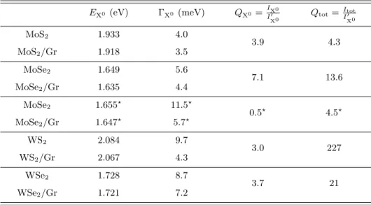
S1. PL PEAK ENERGIES, LINEWIDTHS AND QUENCHING FACTORS
EX0 (eV) ΓX0 (meV) QX0 = IX0 I0 X0 Qtot=IItot0 X0 MoS2 1.933 4.0 3.9 4.3 MoS2/Gr 1.918 3.5 MoSe2 1.649 5.6 7.1 13.6 MoSe2/Gr 1.635 4.4 MoSe2 1.655? 11.5? 0.5? 4.5? MoSe2/Gr 1.647? 5.7? WS2 2.084 9.7 3.0 227 WS2/Gr 2.067 4.3 WSe2 1.728 8.7 3.7 21 WSe2/Gr 1.721 7.2
TABLE S1. Emission characteristics for the samples shown in Fig. 1 of the main text. Peak emission energy (EX0), full width at half maximum of the X0emission line (FWHM, denoted ΓX0) for the PL spectra of the four BN-capped samples discussed in Fig. 1 in the main text, as well as for the sample deposited on SiO2 discussed in Fig. 4 of the main text (data
highlighted with ? symbols). We also consider two PL quenching factors: first, QX0 the ratio between the integrated intensities of the X0 line in TMD (IX0) and in TMD/graphene (IX00); second, Qtotthe ratio between the total PL integrated intensity in
TMD (Itot) and IX00 (that corresponds to the total PL intensity in TMD/graphene). The data were extracted from Lorentzian fits for BN-capped samples and graphene/MoSe2/SiO2 and from a Voigt fit for vacuum/MoSe2/SiO2. Noteworthy, we observe
that ΓX0 is generally smaller on TMD/graphene heterostructures than on TMD, suggesting that graphene further reduces disorder induced broadening and pure dephasing (see also Sec. S2). This effect is particularly striking in our SiO2 supported
sample, since the bare MoSe2 reference does not benefit from BN encapsulation. QX0 remains below 10 in all samples under study and is even smaller than 1 in our SiO2 supported sample.
S2. APPROACHING THE HOMOGENEOUS LIMIT
As shown in Table S1, most of our BN-capped samples display ΓX0 of a few meV and, in any event, significantly
below 10 meV (see Table S1). Considering that τX0 ≈ 2 ps (see Fig. 4,5 and also Sec. S8), we would expect a
lifetime-limited Γmin
X0 = ~/τX0 ≈ 0.3 meV.
Figure S1 shows the PL spectra of another BN-capped MoSe2/graphene sample exhibiting a particularly narrow
ΓX0 down to 2.2 meV. Although ΓX0 remains dominated by broadening due to disorder and dephasing, these results
show that one can approach the homogeneous limit in TMD/graphene heterostructures.
1 . 6 1
1 . 6 2
1 . 6 3
1 . 6 4
1 . 6 5
1 . 6 6
1 . 6 7
P
L
I
n
te
n
s
it
y
(
a
rb
.
u
n
it
s
)
E n e r g y ( e V )
X
0Γ
X 0= 2 . 2 m e V
M o S e
2/ G r
FIG. S1. Narrow PL linewdidth in BN-capped MoSe2/graphene at low temperature. PL spectrum of another
BN-capped MoSe2/graphene sample exhibiting a narrow ΓX0 = 2.2 meV. The spectrum (black circles) was recorded at T = 4 K with a laser photon energy of 2.33 eV and fit to a Lorentzian function (red line). The black arrow at 1.617 eV indicates the expected location of the X?line that is not detectable.
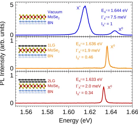
Along this line, we observed that narrow PL linewidth can also be achieved in MoSe2/graphene heterostructures
without the need for an extra BN top layer. In Fig. S2, we report PL spectra of a MoSe2 monolayer deposited
onto boron nitride (BN) and covered only by single (1LG) and bilayer (2LG) graphene. We observe nearly identical and narrow ΓX0, near 2 meV (FWHM) in the 1LG/MoSe2/BN and 2LG/MoSe2/BN heterostructures. The X0 PL
intensity IX0is only quenched by a factor 2.2 in 1LG/MoSe2/BN as compared to the vacuum/MoSe2/BN reference and,
expectedly [53] the X0PL quenching factor Q
X0 (see Table S1) only increases up to a factor of 3 in 2LG/MoSe2/BN.
As we will further discuss in Sec. S9, these results demonstrate that using a single layer of graphene is an optimal solution since X0 emission is already very efficiently filtered with minimal PL quenching (see also Table S1 and Fig. 4
1.56
1.58
1.60
1.62
1.64
1.66
0
1
0
1
0
5
PL In
ten
si
ty
(a
rb
. u
nit
s)
Energy (eV)
2LG MoSe2 BN EX0 =1.633 eV GX0 =2.0 meV IX0 = 0.34 X0 1LG MoSe2 BN EX0 =1.636 eV GX0 =1.9 meV IX0 = 0.46 X0 X0 Vacuum MoSe2 BN EX0 =1.644 eV GX0 =7.5 meV IX0 = 1 X*FIG. S2. Bright, single and narrow line emission in BN/MoSe2/graphene. PL spectra of a MoSe2monolayer directly
deposited on BN (top, blue line), partly covered by a single layer of graphene (middle, orange) and by a bilayer of graphene (bottom, dark red). The X0 exciton energy, linewidth and integrated PL intensity (IX0, in arbitrary units) are indicated. The spectra were recorded at T = 15 K with a laser photon energy of 2.33 eV.
S3. ASSIGNING THE LOW-ENERGY EMISSION LINES IN WSE2 AND WS2
- 1 2 0
- 8 0
- 4 0
0
4 0
- 1 5 0
- 1 0 0
- 5 0
0
5 0
P
L
I
n
te
n
s
it
y
(
a
rb
.
u
n
it
s
)
E - E
X 0( m e V )
W
S e
2X
0X
*X
DL
E - E
X 0( m e V )
X X * / X
DL
W
S
2X
*SX
*TX
0FIG. S3. Photoluminescence lines in WSe2 and WS2. PL spectra of BN-capped WSe2 (left) and WS2 (right) recorded
at 14 K under cw laser excitation at 2.33 eV and 1.96 eV, respectively, as in Fig. 1 of the main text. The origin of the energy axis is taken at the X0 peak energy. The PL spectrum of WS
2is shown on a semi-logarithmic scale for clarity. The low-energy
PL lines below X0 are assigned in keeping with recent reports [10, 16, 54]. XD denotes a spin-dark exciton, X?
S and X?T are
the singlet and triplet trions, XX? denotes a charged biexciton and L refers to localised states, whose physical origin is still
debated. Let us note that exciton-phonon replicas may also contribute to the low energy side of the PL spectra [21]. Also, in the case of WS2, XX?and XD are expected at very close energies [39, 54].
S4. IDENTIFYING THE X0 LINE IN TMD/GRAPHENE HETEROSTRUCTURES
2.00
2.04
2.08
2.12
1.85
1.90
1.95
1.65
1.70
1.75
D
R/R (a
.u.)
WSe2/Gr GX0=7.7 meVEnergy (eV)
WS2/Gr GX0=4.2 meVEnergy (eV)
MoS2/Gr GX0=4.0 meVPL
I
nte
nsi
ty
(a.u
.)
Energy (eV)
FIG. S4. Identifying the X0 line. Differential reflectance (DR) and PL spectra of BN-capped WSe
2/graphene (left),
MoS2/graphene (centre), and WS2/graphene (right) heterostructures, akin to the measurements in Fig. 2f of the main text.
The prominent DR and PL features are assigned to X0. All data were recorded below 20 K in the linear regime under continuous wave (cw) laser excitation at 2.33 eV (MoS2/graphene, WS2/graphene) and 1.96 eV (WSe2/graphene). The full width at half
maximum of the PL spectra ΓX0 are indicated. Note that the data on WSe2 stem another sample than the one shown in
Fig. 1 in the main text. The broad DR feature observed near 1.68 eV in this sample is an artifact arising from the underlying substrate.
1.5
1.6
1.5
1.6
0
50
100
150
200
250
300
1.54
1.56
1.58
1.60
1.62
1.64
Log
10P
L
in
te
n
sity (arb.
u
n
its)
Energy (eV)
Energy (eV)
MoSe
2/
Gr
X* (MoSe
2)
X
0(MoSe
2)
X
0(MoSe
2/
Gr)
Emiss
ion
e
n
e
rg
y (eV
)
Temperature (K)
MoSe
2(a)
(b)
FIG. S5. Temperature dependent PL spectroscopy of the SiO2 supported sample discussed in Fig. 4 of the
main text. (a) Cascade plot of the PL spectra (shown in semi-logarithmic scale) of MoS2 and MoSe2/graphene regions.
(b) Temperature dependent peak energy of the MoSe2 exciton (X0, red circles) and trion (X?, orange squares) lines. The
prominent emission line in the MoSe2/graphene region (green diamonds) lies between these two lines and is assigned to X0,
as also discussed in the main text. The slight (∼ 10 meV) redshift of the X0 line is due to dielectric screening as discussed in Ref. 29 and 37. All data were recorded in the linear regime under continuous wave (cw) laser excitation at 2.33 eV.
0
50
100
150
200
250
300
1.54
1.56
1.58
1.60
1.62
1.64
X* (MoSe
2)
X
0(MoSe
2)
X
0(MoSe
2/
Gr)
E
mi
ssion
e
n
e
rg
y (e
V
)
Temperature (K)
FIG. S6. Temperature dependent PL spectroscopy of the BN-capped MoSe2/graphene sample discussed in
Fig. 1-3 and 5 of the main text. Temperature dependent peak energy of the MoSe2 exciton (X0, red circles) and trion
(X?, orange squares) lines. The prominent emission line in the MoSe2/graphene region (green diamonds) lies between these
two lines and is assigned to X0, as also discussed in the main text. The slight (∼ 10 meV) redshift of the X0 line is due to dielectric screening as discussed in Ref. 29 and 37. All data were recorded in the linear regime under continuous wave (cw) laser excitation at 2.33 eV.
S5. SUPPLEMENTARY DISCUSSION ON THE ABSENCE OF PL FROM TRIONS
S5a. Neutralizing a TMD monolayer with graphene
Different scenarii may explain the absence of X? absorption and emission features in TMD/graphene. Let us first
assume that the TMD coupled to graphene remains doped. Trions may then form rapidly but their slow radiative recombination (in the 20-200 ps range [6, 7]) is quenched by graphene. We may thus still be able to observe an X?
absorption feature in the DR spectra, in contrast with the measurements in Fig. 2e. Furthermore, since the X? PL
feature is more than three orders of magnitude weaker than the X0 PL feature (see inset in Fig. 2f), the X? lifetime
would be reduced to less than ∼ 100 fs, an unrealistically low value. Alternatively, graphene may fully quench hot excitons before they can relax and form X0and X? near resident carriers. However, X? and X0 formation are equally fast in MoSe2(see Ref. [6, 7] and Fig. 4,5). As a result, this scenario would imply massive X0PL quenching, in obvious
contradiction with our observations. The third and most plausible course of events is that all the native dopants in the TMD (either electrons or holes, with a typical density on the order of 1011− 1012 cm−2) transfer to graphene,
leading to a slight increase of the Fermi level of graphene (typically by less than 100 meV) and to the observation of intrinsic absorption and emission. This scenario is corroborated by room temperature Raman scattering [29] and PL measurements (see Fig. S7, S8).
S5b. Evidence for TMD neutralization at room temperature. 1 . 4 1 . 5 1 . 6 1 . 7 1 . 8 1 . 9 2 . 0 2 . 1 2 . 2 2 . 3 1 . 5 1 . 6 1 . 7 1 . 8 1 . 9 X 0 P L I n te n s it y ( a rb .u n it s ) M o S e 2 ( a ) ( b ) ( c ) X * X 02 s B X 0 M o S e 2 / G r E n e r g y ( e V ) M o S 2 / G r x 1 0 0 M o S 2 B X 0 X * 1 . 8 1 . 9 2 . 0 2 . 1 2 . 2 B X 0 ( d ) E n e r g y ( e V ) x 5 W S 2 / G r P L I n te n s it y ( a rb .u n it s ) x 1 0 0 W S 2 X 0 X * X 0 E n e r g y ( e V ) x 1 0 0 W S e 2 / G r W S e 2 X * X 0 X 0 E n e r g y ( e V )
FIG. S7. Trion-free PL spectra at room temperature. PL spectra of BN-capped TMD/graphene heterostructures compared to those of a nearby BN-capped TMD reference, all recorded in ambient air in the linear regime under cw laser excitation at 2.33 eV. The PL spectra in TMD-graphene are quasi symmetric whereas the PL spectra from TMD exhibit a lower energy shoulder that arises predominantly from trions (X?). The scaling factors allow estimating the large room temperature PL quenching factors [29] that strongly contrast with the low X0 PL quenching factors observed at cryogenic temperatures (see main text and Table S1). The X0 lines are slightly redshifted in TMD/graphene, as discussed in the main text, in Fig. S5, S6 and in Ref. 29 and 37. The red lines are multi-Lorentzian fits to the data, with their different components shown with grey dashed lines. Hot luminescence from excited excitonic states (e.g., X02sand B excitons) is clearly visible in
1.8
1.9
2.0
2.1
2.2
10
-210
-110
010
110
-110
010
110
210
310
40
1
1.8
1.9
2.0
2.1
0
1
Energy (eV)
N
orm
al
ized
PL I
nt
ensi
ty
(ar
b.
uni
ts)
PL I
nt
ensi
ty
(ar
b.
uni
ts)
Energy (eV)
WS
2WS
2X*
X
0X
0WS
2/
Gr
WS
2/
Gr
x3
3
x
10
193
x
10
23F
ph(cm
-2s
-1)
(a)
(b)
FIG. S8. Neutrality and photostability under high photon flux at room temperature. (a) Laser power dependent photoluminescence spectra of a BN-capped WS2/graphene heterostructure compared to a nearby BN-capped WS2 reference,
recorded in ambient air using cw laser excitation at 2.33 eV. The spectra are shown on a semi-logarithmic scale and are normalised by the incoming photon flux (Φph) and the integration time. Φph is color-coded with a gradient ranging from dark
red (low Φph ∼ 100 nW/µm2) to yellow (high Φph ∼ 1 mW/µm2). PL saturation due to exciton-exciton annihilation [43]
is clearly visible in WS2, whereas a quasi linear scaling is observed in WS2/graphene. The PL spectra in WS2 remain quasi
symmetric even under high Φph, whereas the PL spectra from the TMD reference exhibit a lower energy shoulder, assigned to
trion (X?) emission. The latter grows significantly as Φphincreases and ultimately overcomes the X0 line, as shown in (b) on
S6. EXCITON BINDING ENERGY
Encapsulation in BN and more generally screening by a surrounding medium significantly reduce the exciton binding energy Eb, as discussed for instance in Ref. 37. In this section, we discuss PL and differential reflectance
(DR) measurements, which allow us to provide a fair estimation of Eb in our samples, also useful to estimate the
changes in exciton radiative lifetime induced by graphene (see Sec. S8.1).
S6a. BN capped MoSe2/graphene
First, on the BN-capped MoSe2/graphene sample discussed in Fig. 2 and 3, we find splittings ∆1s−2s= 110 ± 2 meV
between the X01s and X02s states and ∆1s−3s = 127 ± 4 meV between the X01s and X03s states (see fit in Fig. 3c and
Fig. S9).
0
1
2
3
100
110
120
130
140
D
1s-3sD
1s-2sEne
rg
y
Sp
litt
in
g
(
me
V)
F
ph(x10
23cm
-2s
-1)
BN/MoSe
2/Graphene/BN
FIG. S9. Dielectric screening and reduced exciton binding energy in BN-capped MoSe2/graphene. Splittings
∆1s−2s (black squares) and ∆1s−3s (red circles) between the X01s and the X02s and X03s excitons, respectively. The data are
extracted from the PL spectra shown in Fig. 3a and shown as a function of the cw incoming photon flux at 2.33 eV and T = 4 K.
S6b. BN-supported MoSe2/graphene
We also measured ∆1s−2s ≈ 113 meV and ∆1s−3s ≈ 135 meV using PL spectroscopy (as in Fig. 3 and S9) in
the 1LG/MoSe2/BN sample introduced in Sec. S2 (see Fig. S2). The X02s and X03s features nearly merge into one
slightly asymmetric feature in 2LG/MoSe2/BN and we estimate ∆1s−2s ≈ 109 meV. The reference region of the
sample (vacuum/MoSe2/BN) displays ∆1s−2s≈ 153 meV and its 3s feature merges with the low energy wing of the
hot PL feature from the 1s B exciton (B1s) that is near 210 meV above X0 in all parts of the sample. Interestingly,
although this sample is not covered by a BN thin layer, these energy shifts are very similar to the values reported in Fig. 3 and S9 in a BN-capped sample. These observations suggest that the screening experienced by a ”bare” TMD
monolayer deposited onto a transparent substrate experience is marginally affected by the presence of a top dielectric layer. Let us also stress that sample to sample variations in the energy splitting between excitonic states may reflect various levels of dielectric disorder, as recently investigated in details in Ref. 55.
Echantillon « 2018 » sans BN top
Luis, peux tu vérifier que la calib est la même que sur la diapo 3 ?
100
200
300
EX0= 1.628 eV EX0= 1.633 eV EX0= 1.639 eV X03s X0 2s B1s vacuum/MoSe2/BNPL In
ten
sity (a
rb
. u
nits)
X02s X03s B1s 2D SLG/MoSe2/BNE-E
X0(meV)
X02s+X 0 3s B1s 2D BLG/MoSe2/BNFIG. S10. Dielectric screening and reduced exciton binding energy in BN/ MoSe2/graphene. Hot
photolumi-nescence (similar to the data in Fig. 3) from the 2s (X02s) and 3s (X03s) A excitons as well as from the 1s B excitons in the
BN-supported sample introduced in Sec. S2 and Fig. S2. Note that the X02sand X03s features merge in 2LG/MoSe2/BN. The
energy scale is shown relative to the 1s exciton (X0) energy E
X0. The spectra were recorded at T = 15 K with a laser photon energy of 2.33 eV. The Raman 2D-mode features of single layer and bilayer graphene appear near 2.00 eV, i.e., around 370 meV above the X0 lines.
S6c. BN-capped MoS2/graphene
Similarly, using differential reflectance and PL spectroscopy, we could measure ∆1s−2s ≈ 136 meV and ∆1s−2s ≈
171 meV in BN-capped MoS2/graphene and BN-capped MoS2 sample, respectively, as shown in Fig. S11.
S6d. Discussion
The measured ∆1s−2sand ∆1s−3sin TMD/graphene heterostructures must be compared with the larger splittings
observed TMD samples (see Fig. S9, S2, S11 and Ref. 4, 37, 56, and 57), confirming appreciable reduction of Eb in
TMD/graphene heterostructures. To estimate Ebin TMD/graphene samples, we exploit a very recent study where
1.9
2.0
2.1
2.2
1.9
2.0
2.1
2.2
DR
(arb
.
u.)
B
1sX
01sd(D
R)/dE
(arb
.
u.)
B
1sX
02sX
01sX
02sB
1sI
PL(arb
.
u.)
Energy (eV)
X
01sX*
171 meVX
02sX
03sd(D
R)/dE
(arb
.
u.)
B
1sX
02sX
01sX
02sB
1sDR
(arb
.
u)
136 meVBN/MoS
2/BN
BN/MoS
2/Gr/BN
B
1sX
01sI
PL(arb
.
u)
Energy (eV)
X
01sX
02sMoS2
FIG. S11. Dielectric screening and reduced exciton binding energy in BN-capped MoS2/graphene. From top to
bottom: differential reflectance (DR), its derivative and photoluminescence (PL) spectra (shown in semilog scale) of a BN-capped MoS2 sample (left, blue traces) and a neighboring BN-capped MoS2/graphene region (right, dark red traces). The
relevant excitonic states are indicated by vertical dashed lines. The horizontal dashed lines in the middle panels indicate the zero of the DR derivative. All measurements were done at T = 15 K. The PL measurements were done with an incoming laser photon energy of 2.33 eV.
221 meV were found, respectively, while the 1s-2s splittings were 168 meV and 170 meV, respectively.
Assuming for simplicity that the exciton binding energy reduction is proportional to the reduction of the ∆1s−2s,
we can estimate binding energies Eb≈ 150 meV in our BN-supported and BN capped MoSe2/graphene samples and
176 meV in our BN-capped MoS2/graphene sample, respectively. Our results reveal that one single layer of graphene
significantly reduces Eb by up to ∼ 30 % irrespective of the presence of a BN top layer. Our findings on Eb are
Sample ∆1s−2s (meV) ∆1s−3s (meV) Eb(meV)
BN/MoSe/BN (from Ref. 4) 168 ± 2 - 231 ± 3
BN/Gr/MoSe2/BN (Figs 2, 3 and S9) 110 ± 2 127 ± 4 ≈ 150
MoSe2/BN (Fig. S10) 153 ± 2 180 ± 5 ≈ 210
Gr/MoSe2/BN (Fig. S10) 113 ± 2 135 ± 5 ≈ 155
BN/MoS2/BN (Fig. S11) 171 ± 2 195 ± 5 ≈ 221
BN/Gr/MoS2/BN (Fig. S11) 136 ± 2 - ≈ 176
TABLE S2. Reduced exciton binding energies in TMD/graphene heterostructures. Energy splittings between X0 1s
and X0
2s and (if measurable) X03s states in the samples studied in this work. The estimated exciton binding energies Eb are