Active Optical Clock Distribution
by
Travis L. Simpkins
Submitted to the Department of Electrical Engineering and Computer
Science
in partial fulfillment of the requirements for the degree of
Master of Science in Electrical Engineering and Computer Science
at the
MASSACHUSETTS INSTITUTE OF TECHNOLOGY
May 2002
@
Massachusetts Institute of Technology 2002.
All rights reserved.
A uthor ...
...
Department of Electrical Engineering and Computer Science
May 24, 2002
C ertified by ...
Anantha P. Chandraksan
Associate Professor
Thesis Supervisor
A ccepted by ...
... ...
Arthur C. Smith
Chairman, Department Committee on Graduate Students
BAMKE R
MASSACHUSETTS iNSTITUTE OF TECHOLOGY
Active Optical Clock Distribution
by
Travis L. Simpkins
Submitted to the Department of Electrical Engineering and Computer Science on May 24, 2002, in partial fulfillment of the
requirements for the degree of
Master of Science in Electrical Engineering and Computer Science
Abstract
Clock distribution has become a major problem in integrated circuits. Although clock cycle times continue to decrease, the time allocated to uncertainty in the clock due to skew and jitter has remained constant. Therefore, the percentage of the clock budget devoted to uncertainty has become significant.
One solution to the clock uncertainty problem is to distribute the clock optically. Conventionally, this has involved using a transimpedance pre-amplifier to convert the optical current pulses from the photodetector into voltage waveforms. An inverter-based cascade is then used to amplify the clock pulses into full-swing signals that drive the local clock buffers. Past research has shown that this approach is limited by the imperfect matching of amplifiers from one block to another. Arising from process, voltage, and temperature, these variations can significantly increase the skew, thus negating the benefits of distributing a skewless optical clock.
This thesis will focus on an alternative approach to optical clock distribution. Whereas the cascaded amplifier approach attempts to convert optical current pulses into an electrical waveform, the architecture to be explored in this thesis will use an optical reference clock to deskew an electrical clock. The architecture resembles that of a delay-locked loop (DLL) in that a voltage-controlled delay line is used to synchronize the fully-buffered electrical clock with the optical current pulses from the photodetector. The use of a feedback-based architecture allows the loop to compen-sate for variations due to slow process, voltage, and temperature, and thus minimize skew.
Thesis Supervisor: Anantha P. Chandraksan Title: Associate Professor
Acknowledgments
I would like to thank Prof. Anantha Chandrakasan for his technical contributions to this thesis, as well his guidance and encouragement during the course of the project. It is an honor to have the opportunity to conduct research under a true visionary in the field. This research would also not have been possible without the work of Dr. Paul-Peter Sotiriadis, who provided the transistor-level design of the phase detector and contributed to the architecture. Additionally, I must thank Ben Ruedlinger who offered his optoelectronics experience to the project.
Next, I would like to thank my parents Jerry and Mary Ellen. Their unwavering support of my pursuits over the past twenty-four years is nothing short of amazing. I cannot begin to thank them enough for everything they have done.
Chip design is always a challenging endeavor, and as such, requires the transfer of accumulated knowledge down through the generations of designers. For this reason, I am indebted to Seong-Hwan Cho, Chee We Ng, and Andrew Chen for offering their help and expertise during the design process. I am also appreciative of the support offered by the rest of the research group, including Benton Calhoun, Francis Honore, Alice Wang, Fred Lee, Rex Min, Nathan Ickes, Theodorus Konstantakopoulos, Raul Blasquez-Fernandez, Piyada Phanaphat, and Puneet Newkasar, as well as alumni Manish Bhardwaj, Amit Sinha, and James Kao. I would also like to thank David Wentzloff for his consultations on the art of analog circuit design.
Many people have contributed to my technical development as an engineer. My friends from Suite820-Dan Baker, Aaron Carkin, Kent Lee, Dan Prorok, Ben Ruedlinger, and Steven Troyer-have had a phenomenal influence on my career and my life. I would also like to thank my friends and colleagues at Agilent Technologies in Fort Collins, CO, for jump-starting my career in chip design over the course of two summer intern-ships. I am particularly indebted to my mentor-manager, Stephen Clarke, who has repeatedly offered his technical expertise, both to my projects at Agilent and to my research at MIT.
Prof. David Smith, Paul Maccoux, Jeff Tracey, Ray Rosenberry, Jim Duxbury, James Powell, Bill Yerman, Joyce Fast, David Tibbitts, and the staff of Oak Street Elemen-tary in Orrville, OH.
Finally, I am also grateful to the National Defense Science and Engineering Gradu-ate Fellowship (NDSEG) and to MARCO for financial support throughout the project.
Contents
1 Introduction
1.1 Background . . . .
1.1.1 Electrical Clock Distribution . . . .
1.1.2 Optical Clock Distribution . . . .
2 Architecture of the Optical Deskew
2.1 System Operation . . . .
2.2 The Local Controller . . . .
2.3 The Delay Line . . . .
2.4 Stability of the ODB Architecture .
3 Circuit Implementation o 3.1 Circuits of the Local Co
Buffer
f the Optical I ntroller . .
eskew Buffer
3.1.1 The Phase Detector . . . .
3.1.2 Amplifiers . . . .
3.1.3 Latched Comparator . . . .
3.1.4 Control Block . . . .
3.1.5 Charge Pump . . . .
3.1.6 Local Controller Synchronization
3.2 Circuits of the Delay Line . . . .
3.2.1 Bias Generator . . . . 3.2.2 Delay Elements . . . . 3.2.3 Differential-to-Single-Ended Converter 17 18 18 20 23 24 24 29 29 31 31 32 32 34 36 37 38 40 41 42 44
3.3 Local Controller and Delay Circuits Interaction 3.4 Auxiliary Components . . . .
3.4.1 Current Pulse Generator . . . .
3.4.2 Ring Oscillator . . . .
3.4.3 XOR Phase Detector . . . .
4 Optoelectronics
4.1 Background . . . .
4.2 Lateral-PIN Photodetectors . . . .
4.3 Implementation . . . .
5 On-Chip Measurement of System Performance 5.1 Background . . . .
5.2 Previous Work . . . . 5.2.1 Time-to-Voltage Converters . . . .
5.2.2 Time-to-Digital Converters . . . .
5.3 Overview of the Time-to-Digital Converter . . .
5.4 Time-to-Digital Converter Implementation . . .
5.4.1 Operation of the TDC . . . . 5.4.2 Resolution and Calibration . . . .
5.5 Sum m ary . . . .
6 The Test Chip
6.1 Dual-Optical Deskew Buffers .
6.1.1 DODB Results . . . . .
6.2 Closed-Loop Simulated Pulsing
6.2.1 CLSP Results . . . .
6.3 Summary . . . .
7 Conclusions
7.1 R esults . . . .
7.2 Performance Limitations of the ODB Architecture . . . .
. . . .
. . . .
. . . .
. . . .
. . . .
. . . .
. . . .
. . . .
46 48 49 49 51 53 53 54 56 59 60 61 61 61 62 63 66 68 68 71 72 74 7677
81 83 83 847.3 Summary ... ... 86
7.4 Future W ork . . . . 86
7.4.1 Optoelectronics . . . . 87
7.4.2 Circuitry . . . . 87
7.4.3 Testing . . . . 88
A Test Chip Implementation Details 89 A.1 Open-Loop Simulated Pulsing . . . . 89
A.1.1 OLSP Results . . . . 91
A.2 Layout Techniques . . . . 93
A .3 Sum m ary . . . . 93
List of Figures
1-1 Illustration of skew and jitter. . . . . 17
1-2 Balanced H-tree clock distribution network. . . . . 19
1-3 Intel deskew buffer (IDSK) architecture [6] . . . . 20
1-4 Optical clock distribution using waveguides [9]. . . . . 21
1-5 Transimpedance amplifier-based optical clock distribution. . . . . 21
2-1 Optical deskew buffer architecture. . . . . 24
2-2 Local controller block diagram. . . . . 25
2-3 Illustration of A. lead, B. lag, and C. locked with the corresponding phase detector output. . . . .25
2-4 T im ing. . . . . 27
2-5 ODB modes of operation. . . . . 28
3-1 Block diagram of phase detector. . . . . 32
3-2 Fully-differential offset-cancelling switched capacitor amplifier. .... 33
3-3 Timing diagram of the switched-capacitor amplifier. . . . . 33
3-4 Latched comparator. . . . . 35
3-5 Timing diagram of the latched comparator. . . . . 35
3-6 Control block. . . . . 36
3-7 Charge pump schematic. . . . . 38
3-8 Amplifier and comparator timing diagram. . . . . 39
3-9 Clock generation block. . . . . 40
3-10 Delay circuits block diagram. . . . . 41
3-12 D elay line. . . . . 42
3-13 Delay elem ent. . . . . 43
3-14 Normalized delay vs. control voltage. . . . . 44
3-15 Normalized delay vs. Up pulses received by the charge pump. .... 45
3-16 Differential-to-single-ended converter. . . . . 46
3-17 Control voltage of ODB while in lock. . . . . 47
3-18 Current pulse generator. . . . . 49
3-19 Ring oscillator. . . . . 50
3-20 Ring oscillator and delay line. . . . . 50
3-21 XOR phase detector . . . . 51
4-1 Cross-sectional structure of a typical lateral-PIN photodetector. . . . 55
4-2 Layout of a single finger of the photodetector. . . . . 56
4-3 Layout of the complete photodetector. . . . . 57
4-4 Cross-sectional structure of the implemented photodetector. ... 58
5-1 Illustration of skew. . . . . 60
5-2 TDC overview. . . . . 62
5-3 TDC simplified timing diagram. . . . . 63
5-4 TDC block diagram. . . . . 64
5-5 TDC schem atic slice. . . . . 65
5-6 TDC timing diagram. . . . . 67
6-1 Dual-Optical Deskew Buffer (DODB) architecture . . . . . 72
6-2 DODB simulation results showing the control voltages of each ODB. . 74 6-3 Normalized phase of each ODB local clock output. . . . . 75
6-4 Closed-Loop Simulated Pulsing (CLSP) architecture. . . . . 76
6-5 CLSP system control voltage and XOR phase detector output. . . . . 77
6-6 CLSP reference clock and local clock phase relationship during acqui-sition and lock modes. . . . . 78 6-7 CLSP system control voltage while in lock, showing quantization noise. 79
6-8 CLSP power consumption. . . . . 80
A-1 Open-Loop Simulated Pulsing (OLSP) architecture. . . . .
90
A-2 O LSP results. . . . .
92
A-3 Layout of the chip. . . . .
95
List of Tables
1.1 Variation induced skew in optoelectronic circuits...
3.1 Delay line dynamic range at 100 MHz, 1.8 V, and 25 'C.
4.1 Photodetector design summary . . . .
5.1 5.2 6.1 6.2 6.3 A.1 A.2 A.3 TDC design summary TDC pins . . . . DODB pins . . . . CLSP pins . . . . Simulated results . . . OLSP pins . . . . Test chip summary . . Other pins . . . . 22 42 58 68 69 73 81 81 91 94 94
. . . .
. . . .
Chapter 1
Introduction
Clock distribution has become a significant challenge in VLSI design. Modern micro-processors contain tens-of-thousands of synchronous elements whose correct operation relies upon the distribution of a precise clock. Traditionally, the primary means of increasing the performance of these devices has been to increase the clock rate, or equivalently, to decrease the clock cycle time. Therefore, the maximum operating fre-quency of a device occurs when the slowest sequence of register-bounded logic gates can just complete execution within the corresponding cycle time. For this reason, it is advantageous to fully utilize the entire clock period. In typical systems, however, the full clock period cannot be devoted to logical operations due to imperfections in the clock waveform, commonly known as skew and jitter.
Whereas skew refers to the static phase difference between the clock signals at two unique points in the network, jitter refers to the tendency for a particular clock edge to dynamically shift either forward or backward in time. Fig. 5-1 illustrates the difference between skew and jitter. Together, skew and jitter are known as clock
+-T
= 8 ns
1|+T = 8 ns
-I I I |I
Skew =1 ns
Jitter
=
0.5 ns
uncertainties and often account for as much as 10% of the clock budget in a modern microprocessor.
With technology scaling, propagation delays have likewise decreased, thus lead-ing to higher clock frequencies and greater performance. Uncertainties in the clock waveform, however, have remained generally constant. When combined with shorter cycle times, constant amounts of skew and jitter have led to increased portions of the timing budget being devoted to uncertainty. Recently reported figures indicate that during Intel's transition from .18 ptm to .1 pm technology, the skew budget increased by 37%[1].
This chapter will discuss the background and motivations for the work presented in this thesis. A discussion of the previous work in both electrical and optical clocking will be presented in this chapter.
1.1
Background
Since the creation of microprocessors in the 1970's, electrical clocks have been used to coordinate the operation of the various synchronous elements contained on the integrated circuit. This approach has proven widely successful across many genera-tions of designs and architectures. As frequencies increase beyond 10 GHz, however, electrical clocks are expected to become far less reliable, thus threatening the future development of high-speed designs[1).
In anticipation of this obstacle, alternative clock distribution schemes have been considered. Possibly the most promising, optical clock distribution was first proposed in 1985 [2, 3]. Although significant research has been conducted since that time, opti-cal clocking has yet to be successfully demonstrated on a commercial microprocessor.
1.1.1
Electrical Clock Distribution
To help reduce skew, many microprocessors use a hierarchical clock distribution scheme based on a balanced H-tree network as shown in Fig. 1-2 [4, 5]. This ap-proach uses additional buffers at each level of the hierarchy to provide the proper
Figure 1-2: Balanced H-tree clock distribution network.
amount of drive strength. Since all of the buffers at a given level are driven by the same higher-level buffer and are located equidistant from this buffer, the clock edges transmitted from the higher-level buffer theoretically arrive simultaneously at each local buffer. Although careful routing can ensure that the H-tree is designed in a perfectly balanced manner, process variations during fabrication now produce enough imperfections that their effects are significant. For this reason, basic H-tree distribution schemes are becoming less viable for clock distribution.
One solution that compensates for the imperfect H-tree distribution networks is to deskew the clock at the second level buffers[6, 7] as shown in Fig. 1-3. Proposed by Intel and implemented on the IA-64 microprocessor, this approach distributes two clocks in symmetric H-trees. One of the clocks is the global core clock while the other clock is a reference clock that sees a fixed load and undergoes less buffering. These characteristics cause it to experience less skew than the primary global clock. At the local level, the reference clock is used to deskew, or synchronize, the global clock before being distributed to the local clock domain via a clock grid. The deskewing, however, is only performed upon startup; once the local clock is synchronized to the reference clock, the deskewing operation ends. As a result, this approach can compensate
RCD
Deskew Buffer MMMMM
- Delay
-Global Clock 1 Circuit I Regional
Clock Grid
TAP I/F ~:i
ii
Ref. Clock I I .]-MM
S Local ControllerRC
Figure 1-3: Intel deskew buffer (IDSK) architecture [6].
for process-induced variations in the H-tree distribution network and the higher-level buffers of the global core clock. To increase the stability of the system, Intel currently stops deskewing once the startup phase is complete. Therefore, the IDSK does not presently compensate for skew induced by dynamic voltage and temperature gradients, or for a time-varying load. Using this approach, Intel has reported a a 75% reduction in skew from 110 ps to 28 ps [6].
1.1.2
Optical Clock Distribution
One commonly proposed solution to the clock skew problem is to distribute the clock
optically [2, 3, 8]. In such a system, an off-chip optical source, such as a laser,
generates a pulse train of photons at the desired frequency. These optical pulses are then distributed across the chip, either using off-chip holographic distribution or optical waveguides on-chip, to the local clock domains where they are converted into a conventional electrical clock. Fig. 1-4 shows one possible implementation of optical clocking in which the traditional H-tree topology is still employed, first to distribute the optical pulses, and later to distribute the electrical clock after the optical-to-electrical conversion has occurred. However, since the highest level of the hierarchy involves photons traveling through optical waveguides rather than electrons in metal routes, virtually no skew is introduced. Once the photons reach the end of the top-level waveguides, they are converted to electrical pulses before being further
waveguides
rec eiver
circuitry
electrical
clock
distribution
Figure 1-4: Optical clock distribution using waveguides [9].
distributed to synchronous elements in the local block.
The conversion of the optical current pulses to voltage waveforms is performed
by a transimpedance amplifier (TIA) [10]. Since the waveforms out of the TIA are
typically not full swing, a cascade of voltage buffers are used to amplify the pulses into
logic-level signals. A block level diagram of this transimpedance-based architecture
is shown in Fig. 1-5. The problem with this approach is that it requires excellent
Cok Local Cloc~k
Photodetector
Reverse Bias
Table 1.1: Variation induced skew in optoelectronic circuits.
Variation Source Skew
-10% VDD 24 ps
+50 0C 18 ps
+10% Lp01y 80 ps
-10% Vt 70 ps
matching between the amplifiers that are located across the chip. Variations arising from process, voltage, and temperature combine to create skew between the local clock domains. Recently reported figures for this skew are shown in Table 1.1 [11].
Research has shown that these variations can nullify nearly all of the gains associated with distributing an ideal optical clock [12].
Chapter 2
Architecture of the Optical Deskew
Buffer
The architecture of the optical deskew buffer resembles that of Intel's deskew buffer (IDSK) [6]. Both are modeled after a traditional delay-locked loop architecture in which the output clock is synchronized to an input clock. Likewise, both systems utilize a local controller and a delay line to accomplish the deskewing operation.
At this point, however, the similarities end. Whereas the IDSK uses an electrical clock as the reference, the Optical Deskew Buffer (ODB) presented here utilizes an optical clock for this purpose. Using an optical clock for the reference allows for further reduction in the skew arising from mismatches in the reference clock H-tree. The two systems also differ in when the deskewing is performed. In the case of the IDSK, deskewing only takes place during the startup sequence of the microprocessor, while the ODB performs continuous deskewing of the global clock. By deskewing continuously, the ODB is able to compensate for skew induced by process variations as well as slowly changing voltage and temperature gradients. As it is currently implemented, the IDSK can only compensate for process-induced skew, although the architecture is reportedly capable of continuous deskewing.
The remainder of this chapter will discuss the details of the architecture and operation of the optical deskew buffer.
Optical
Reference Clock
Photodetector
Loca Cotrlle
Global Electrical Clock
Variable
Local Clock
Delay Circuits
Figure 2-1: Optical deskew buffer architecture.
2.1
System Operation
The ODB synchronizes an electrical local clock to an optical reference clock by sam-pling the local clock and adjusting the amount of delay added to the global clock, such that the local clock becomes matched in phase to the reference clock. The local controller directs this operation. By comparing the optical current output from the photodetector with a feedback version of the local clock, the local controller deter-mines whether the local clock leads or lags the optical reference. The local controller then either increases or decreases the control voltage of the delay line accordingly. When the local clock is synchronized with the optical clock, the ODB has attained lock, and the control voltage of the delay line is maintained. The local controller does not stop sampling its inputs, however. If fluctuations in voltage, temperature, or load should cause changes in the skew, the local controller issues corrections to the delay line to compensate for these variations in the phase. Therefore, the ODB employs active deskewing.
2.2
The Local Controller
The local controller integrates the functions typically performed by the phase detector and charge pump of a traditional DLL. The operation of the local controller begins
Optical Reference Clock
Feedback F'Phase Apier >Mrfe Latched Charge Control Voltage Local ClockL. Detector Apfir Apfer Comparator-, Control Pump Lo
Capacitor
Figure 2-2: Local controller block diagram.
with the phase detector which continuously compares the feedback local clock to the optical current output from the photodetector. The output of the phase detector is a fully-differential small-signal voltage that is proportional to the phase difference of the input signals. This voltage is then amplified in two fully-differential offset-canceling switched-capacitor amplifiers before being latched in a comparator. The function of the comparator is to convert the amplified analog voltage representing the phase difference into a digital CMOS-level output. A block diagram of the local controller is shown in Fig. 2-2.
The phase detector outputs a voltage that indicates whether the electrical input leads or lags the optical input as illustrated in Fig. 2-3. Since the goal of the ODB is to align the respective clock edges, a lead signal should result in more delay being added to the global clock while a lag signal should reduce the delay. As shown in Fig. 2-3 C, the phase detector considers the clocks to be in lock when they have a
phase offset of 900, and thus the phase detector performs quadrature locking. This
condition is a result of the characteristics of the phase detector, and does not affect the performance of the system.
Given a random phase relationship of the inputs, the probability of receiving
Optical Reference Current LJL' Local
m_
Clock L :7
Y
PD Output-1 ---..---PD Output_2 ...-----Leading
Lagging
Locked
Figure 2-3: Illustration of A. lead, B. lag, and C. locked with the corresponding phase detector output.
either a lead or lag signal from the phase detector is 50%. This random phase state is exactly the condition that occurs upon startup since the phases of both the electrical and optical inputs to the phase detector are unknown. Therefore, if the output of the comparator is directly used to control the charge pump, a condition could occur upon startup in which the charge pump is instructed to decrease the voltage of the loop capacitor. Of course, since the system has just started, the voltage on the capacitor is already zero, and hence, the charge pump will be unable to lower it further. With the control voltage fixed at zero, the phase of the local clock will remain the same, and hence, this condition will be terminal.
Since the problem arises because the loop capacitor is initially at a voltage of zero, the solution is to increase the control voltage regardless of the output of the phase detector. Therefore, the Local Controller always attempts to align the clocks by adding delay to the global clock. In terms of Fig. 2-3, this means that the global clock will be continuously shifted to the right until the edge of the local clock properly aligns with the reference clock. To add this capability, a control block of digital logic is inserted between the comparator and the charge pump.
The process just described is depicted in Fig. 2-4. The top plot in the figure shows the reference clock and the local clock. At the start, the local clock slightly lags the reference. The corresponding phase detector output is shown in the second plot. Due to the relative position of the A and B outputs, the comparator issues a Down signal. The control block overrides this signal, however, and issues an Up signal to the charge pump. By time M, the global clock has been delayed sufficiently far that the outputs of the phase detector are now flipped, and hence, the commands issued by the comparator now match those of the control block. At time N, the edges of the two clocks are properly aligned, and the loop is locked.
Just as it is important to begin unconditionally charging the loop capacitor upon startup, it is also critical to know when to exit this process and begin controlling the charge pump based on the output of the comparator. Since the preprogrammed routine will eventually result in the comparator issuing an Up command, the control block should relinquish control when the comparator issues an Up followed
immedi-Reference Cloc B ... .. .. .- .. ... -I ime 0-0 M N Time Comparator Signal
Signal L AAAALL AALAAAAA AALAAAA.A.AL.L
Figure 2-4: Timing.
ately by a Down command. When this Up/Down sequence is detected, the system has entered lock, and the control voltage should be maintained at its present level. From this point onward, the control block will forward the signals from the phase detector to the charge pump, and thus allow the system to continue adjusting the delay to compensate for future changes in the skew due to voltage, temperature, or load variations.
The second role of the control block is to decrease the acquisition time of the ODB. Typically defined as the amount of time it takes for the system to obtain lock after starting from a known initial state, acquisition time represents idle time for the digital elements of the microprocessor since no useful computation can be performed during this period. Since microprocessors generally initiate the startup sequence infrequently, acquisition time is of less importance for PLL/DLLs found in these systems. Nevertheless, it is still desirable to minimize the acquisition time to
Reset I Acquisition I Lock
Mode I Mode Mode
a| 0) 0 Time Turbo Reset
Figure 2-5: ODB modes of operation.
some extent.
Since the Up/Down sequence from the comparator indicates that the system is approaching lock, this sequence can also be used to change the amount of charge delivered by the charge pump onto the loop capacitor. By enabling a special mode upon startup, the charge pump delivers large quantities of charge initially, which causes the loop to approach lock faster. Once in lock, smaller quantities of charge are delivered to reduce the phase noise of the system. This leads to three logical modes of operation as shown in Fig. 2-5. While Reset is asserted, the loop capacitor is grounded, thus negating the effect of either Up or Down pulses. When Reset is deasserted, the system enters acquisition mode in which the control block begins unconditionally charging the loop capacitor. During this mode, the Turbo signal is asserted so as to reduce the acquisition time by increasing the amount of charge delivered by the charge pump. When the edges of the reference clock and the local clock are properly aligned, the system enters lock mode in which the phase detector continually monitors the phase of the system, and issues corrections as necessary.
detector has compared the electrical input to the optical input and the control block has operated the charge pump accordingly. The loop capacitor stores the charge from the charge pump, and serves as the link from the local controller to the delay line. Implementation details for the loop controller will be discussed in the next chapter, while the next section will describe the operation of the delay line.
2.3
The Delay Line
Since the loop controller always issues Up commands while approaching lock, the delay line needs to be able to provide exactly one period of delay in the worst case. To allow the system to compensate for voltage, temperature, and load variations, however, added dynamic range is needed, which is provided by adding more delay
stages. So long as this dynamic range requirement is met, any type of
voltage-controlled delay line is compatible with the system. Since the ODB architecture performs clock synchronization rather than clock generation, the local clock output jitter will be at least as large as the global electrical clock input jitter. In other words, the ODB must accept the jitter generated upstream, but should strive to minimize the jitter added at this level. For this reason, the Maneatis self-biased architecture was selected for the delay elements, as well as the accompanying bias circuitry, differential-to-single-ended converter, and charge pump [13, 14]. Combined, these elements have been shown to exhibit low jitter, high power-supply rejection, and high substrate noise rejection. Implementation details of these circuits will be provided in Chapter 3.
2.4
Stability of the
ODB
Architecture
Delay-locked loops have been shown to be first-order systems, meaning that they are generally stable by design. Since the ODB is based on a DLL-type architecture, stability is not a significant issue. Nevertheless, stability problems can occur in DLLs if the control voltage of the delay line is updated without knowing the results of the
previous correction. Designing the system such that it waits longer before sampling the inputs and issuing corrections is commonly referred to as "slowing down the loop," and can generally be used to avoid stability problems in DLLs.
Due to the characteristics of the phase detector in the local controller, it is im-portant to limit the rate at which corrections to the control voltage are administered. While the phase detector continually compares the local clock to the reference clock, it cannot respond instantly to changes in phase. Therefore, the phase detector must be given adequate time such that its outputs reflect the phase relationship of its inputs. This is accomplished by having the amplifiers and comparator sample the outputs of the phase detector at a rate much lower than the global clock.
The slower sampling rate is also necessary to insure that the amplifiers have time to settle between each stage of the sampling. Specifically, the outputs of the first amplifier must have settled before the second amplifier samples its inputs. Likewise, in order for the comparator to accurately latch the input, the outputs of the second amplifier must have first settled. Finally, adequate time must be allocated for the amplifiers to reset before the next sampling cycle begins.
Chapter 3
Circuit Implementation of the
Optical Deskew Buffer
This chapter will describe the circuit implementation of the optical deskew buffer. The target process for the design was the TSMC .18 pm Logic process, as available through MOSIS. Discussion will follow the pattern established in the previous chapter; it will start with the local controller and proceed to the delay line. The chapter will conclude with a description of auxiliary circuit blocks not fundamental to the ODB itself, but useful during the test chip implementation.
3.1
Circuits of the Local Controller
The local controller consists of five discrete circuit blocks, namely the phase detector, amplifiers, latched comparator, control, and the charge pump. Although many of these blocks contain analog circuitry, they require precise synchronization to function properly. The following subsections will present the circuitry of each block, as well as a timing diagram of its operation. An overall timing diagram of the entire local controller controller will then be presented to explain the interaction of the various blocks.
3.1.1
The Phase Detector
Schematic design of the phase detector was completed by Paul-Peter Sotiriadis. For this thesis, this circuitry will be considered a blackbox which accepts a pair of non-overlapping differential electrical clocks and one optical reference clock in the form of current pulses. As shown in Fig. 3-1, it produces a pair of small-signal differential signals proportional to the phase difference of the inputs. The common-mode output of the phase detector is proportional to the magnitude of the optical current input by a 10:1 ratio. With optical current of ~2 pA, a common-mode output of ~20 mV is expected. Layout of the device was completed as part of this thesis.
3.1.2
Amplifiers
Since the outputs of the phase detector are small-signal, significant amplification is necessary before the signals can be latched in the comparator. The amplifiers were specifically designed to exhibit minimum input offset voltage, high power-supply re-jection, high common-mode rere-jection, and good noise performance. By using smaller transistor sizes, input capacitance of the amplifiers was minimized in order to match the drive capabilities of the phase detector. The frequency response of the amplifiers was not a design concern since the inputs are basically DC signals. Settling time, however, was considered, since the outputs of the system should be stable before the comparator latches. This was a flexible design specification since the sampling rate of the comparator can be slowed to accommodate the settling time of the amplifiers.
Nonetheless, a settling time of 20 ns was targeted for the amplifier.
Optical Reference Current
Electrical Clock
Phase
Output
(Differential)
Detector
(Differential)
Vdd Clk Clk CMControlW L =.;It InA InB
M
2 =18 MCIk
. pF W.2=72 2 pFCIkc
W=.72 W72 1=360 =.38 Clkc~ -- Ck Vdd Vdd W. vb2 OutA OutB L =36 W=4 b3 W. =.36 L .b3 W.I
Vdd ICMControl
I
vb2
W=3W. L =36 =.36V W22H AF=10.0 vb3 V~ =.3 W=.3 vb2-
WW
2
Figure 3-2: Fully-differential offset-cancelling switched capacitor amplifier.
Ck
CI kc
InA
---InB
OutA_
OutB
- -- --A cascade of fully-differential offset-canceling switched capacitor amplifiers was
implemented to meet these requirements. Each stage was designed to provide a gain of A, 1 10, such that when cascaded, the overall gain would be A, ~ 100. The fully-differential topology of the amplifiers was selected for its good common-mode noise rejection. A switched-capacitor offset-cancellation scheme was employed to minimize the input offset voltage. To reduce thermal noise, PMOS inputs were used for the amplifier, at the expense of a lower gm. To reduce the output impedance, and therefore minimize the charge-injected coupling from one stage to the next, an output buffer was added to the design. The schematic of a single amplifier is shown in Fig. 3-2
Switched-capacitor amplifiers are derived from sample-and-hold circuits and there-fore, require precise synchronization to insure proper operation. Fig. 3-3 shows a basic timing diagram for the switched-capacitor amplifier. When Clkc is asserted, the amplifier is in the reset state. At this time, nodes ni and n2 are connected to the common mode input voltage while nodes n3 and n4 are shorted to the output. This feedback configuration allows the amplifier to adjust the voltage of nodes n3 and n4 such that current through each side is symmetric and the outputs are matched. Once this balanced state has been attained, the resulting voltages at nodes n3 and n4 are equal to the offset voltage of the amplifier. When Clkc is deasserted, the common mode input is disconnected and the offset voltage is "stored" on the capacitor. Like-wise, when Clk is asserted, nodes n1 and n2 are connected to the source signals, which in turn causes nodes n3 and n4 to respond proportionally. The amplifier is now in the amplify state, and the outputs adjust to reflect the relative level of the inputs.
3.1.3
Latched Comparator
By detecting which of its two inputs has a higher voltage, the latched comparator,
shown in Fig. 3-4, acts as a sense-amplifier followed by an RS-latch. The circuit was designed to have minimum input capacitance, low input offset, and a reasonable settling time. Ideally, a latch with no offset voltage would be preferred.
Vdd
~T
ClockCompA
,,ClockCompA
L =.36 L =.36 L =.36 L =.36R
S
CompU
InA
=.444InB W.4"4Comp D
ClockComp
1
.4=.80
Figure 3-4: Latched comparator.
by two clocks. A timing diagram of the circuit is shown in Fig. 3-5. During the
precharge state, ClockComp and Clock-CompA are low, and nodes R and S are
precharged to Vdd. When ClockComp and Clock-Comp-A transition high, the latch
enters the sample state. Depending on which of the inputs is stronger, either node R or S will be pulled down. The positive feedback provided by the cross-coupled transistors insures a fast execution of this event. Since nodes R and S are connected to the inputs of an RS-latch, the downward going transition on node R or S has the
CIk_CompA ClkComp InA InB S CompD
effect of setting or resetting the latch. These values are then stored until the inputs
of the comparator change, even when the comparator enters the precharge state.
3.1.4
Control Block
The control block is designed to accept the inputs from the latched comparator and
produce the Up and Down pulses for the charge pump. Due to the characteristics
of the system described in Chapter 2, the control block also regulates whether the
system is in the acquisition or locked mode of operation, and thus whether the outputs
of the latched comparator are used to control the charge pump.
-- CompU Y D Q NRS C ub )p B s
~leDFF
Reset Reset -->
CK QN--Vdd UPC CompU B Up Control Pulse Down -- CompD A Downc Control Clkln PulseFigure 3-6: Control block.
The control block, shown logically in Fig. 3-6, uses a few simple storage elements
to track the outputs of the latched comparator, and thereby determine the mode of
operation. Specifically, the control block looks for the latched comparator to issue an
Up signal followed immediately by a Down signal. (Recall that the latched comparator
has differential outputs, such that exactly one of the Comp U or CompD outputs is
always asserted, indicating the intended signal.) The first D-type flip-flop (DFF)
of the upper path stores the output of the Up signal from the comparator. When the output of this DFF and the current Down signal are both asserted, the desired
Up/Down sequence has been detected and the system changes from the acquisition to
the locked state. The RS flip-flop then stores this state and outputs the appropriate
Control signal. The Turbo signal is easily generated as well.
The second path of logic generates the control pulses used to direct the operation of the charge pump. The top multiplexor and its ensuring logic generate the Up signal and its complement, Upc. If the system is in the acquisition state, the Control signal directs the multiplexor to sample a logical Hi (VDD). Therefore, when the
Pulse signal arrives at the NAND gate, an Up pulse is issued to the charge pump.
Conversely, when the system is in the locked state, the Control signal causes the output of the comparator to be sampled when the Pulse signal arrives. The lower multiplexor performs the same operation except that it accepts the CompD signal from the comparator as well as a logical Lo (GND), and outputs the Down and Downc signals to the charge pump.
The final path of logic in the block accepts the system control clock, which is the same clock as used by the first amplifier, and outputs a short Pulse signal used by the DFFs and the NAND gates within the block. The width of the pulse is determined
by the number of inverters preceding the NAND gate, and is currently set to produce
a pulse of -200 ps. Since the Up and Down pulses delivered to the charge pump are derived from this pulse, the charge delivered by the charge pump will be directly proportional to its width.
3.1.5
Charge Pump
The charge pump is based on the offset-cancelled charge pump published by Maneatis and is shown in Fig. 3-7 [13, 14]. When an Up pulse is received, node n1 is momentar-ily pulled down, which causes a burst of charge to be deposited on the loop capacitor. Conversely, when a Down pulse is received, charge is removed from the loop capacitor. Since the charge pump and the delay line interact closely, a feedback signal, VBn, is used to dynamically adjust the amount of charge transferred based on the state
of the delay line. This helps to insure that each Up or Down pulse causes an equal amount of delay to be added or subtracted from the global clock. Therefore, as VBn decreases, the charge transferred by the circuit during each pulse decreases, but the relative adjustment in delay is the same.
Vdd
Control
Up UPC Downc Down Reset
Loop Capacitor
Turbo VBn VBn Turbo
Figure 3-7: Charge pump schematic.
The topology differs from the Maneatis version in that two extra transistors have been added to provide a Turbo mode of operation. In this mode, the charge pump de-livers more charge per pulse to the loop capacitor, thus decreasing system acquisition time. Additionally, a path to ground was added to provide a means of discharging the loop capacitor during testing.
3.1.6
Local Controller Synchronization
The preceding sections have presented the various circuits of the local controller as well as timing diagrams of the signals needed for their operation. To function properly, however, each of these blocks must be precisely synchronized with the others. A timing diagram showing the complete operation of the local controller is provided in Fig. 3-8.
The sequence of events begins when the first amplifier samples the outputs of the phase detector. While the first amplifier is holding its outputs, the second ampli-fier samples and further amplifies these signals. Finally, after the second ampliampli-fiers' outputs have settled, the comparator latches and the amplified output of the phase
T/4 rOl- - - - - - --- - - - ---- 4~ . -ClkAmp_ CtkAmp_2 ClkCompA
_ L
Clk_Comp F PhaseDtecor 80P O tputs .-. r ... ... .... O~pts... ... .. -.- -- --- - -- s- -CornpU CompD UP DN Control Voltage (Analog)Figure 3-8: Amplifier and comparator timing diagram.
detector is stored as Comp U and CompD. As the figure shows, Comp U and CompD
only transition during cycles when the outputs of the phase detector change. At all
other times, their values remain constant. The rising edge of the first amplifier clock
also causes the control block to issue a correction to the charge pump. Depending on
whether this pulse is an Up or a Down, the charge pump either delivers or removes
charge from the loop capacitor, causing its voltage to rise or fall.
Six clocks are used to synchronize the operation of the local controller. Each of the
amplifiers require two differential non-overlapping clocks and the comparator requires
two clocks, one being a slightly advanced version of the other. Since the amplifiers,
comparator, and charge pump are designed to operate in a nested fashion, the phase
and duty-cycle of the clocks is critical. While the phase and duty-cycle of each clock
vary, the frequency of the clocks are identical and is equal to the feedback rate of
the system. The feedback rate controls the rate at which the local controller makes
corrections to the amount of delay being added to the global clock. As implemented,
the feedback rate is set to 1:512 meaning that the local controller updates the control
voltage of the delay line once for every 512 cycles of the global clock.
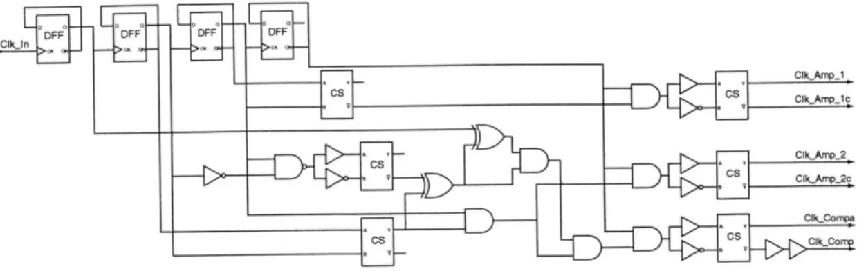
Figure 3-9: Clock generation block.
The top row of DFFs is used to divide the global clock. For simplicity, only four
DFFs are shown, although the actual implementation would require nine to produce
the 1:512 feedback ratio. The block labeled CS in the schematic is a clock-separation
block based on an RS flip-flop. It is used to generate non-overlapping clocks from
purely differential clocks. Essentially, it "separates" the clock pulses in time, and thus
is referred to as a clock-separator. These non-overlapping clocks prevent glitches from
occuring during the various logical operations performed in the block. The output
clocks of the block are shown in the timing diagram of Fig. 3-8.
3.2
Circuits of the Delay Line
The delay line and supporting circuits are based on the self-biased architecture
pub-lished by Maneatis [13, 14]. This includes the bias circuit, delay elements, and
differential-to-single-ended converter as shown in the block diagram of Fig. 3-10.
As with the local controller, the layout of the delay line employed spherical
common-centroid layout wherever possible in order to increase matching. The self-biased
topology of the Maneatis architecture increases the symmetry of the design, and
therefore is quite amenable to this type of layout. The following sections will discuss
the topology as it pertains to the 0DB, with particular attention devoted to any
modifications made.
ConrolBn, Bp
Global Clock
(Differential) Differential-to Local Clock
10 Delay Line Single Ended
Converter
Figure 3-10: Delay circuits block diagram.
3.2.1
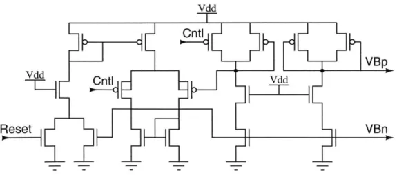
Bias Generator
The bias generator was implemented exactly as described by Maneatis and is shown
below in Fig. 3-11 [13, 14]. This block receives the control voltage from the loop
capacitor as its input, and generates two bias voltages, VBp and VBn, as outputs.
The VBp output is a buffered version of the control voltage, and typically tracks it
over the operating region of the circuit. VBn is basically the complement of VBp
since it inversely tracks the control voltage. Since the control voltage of the system
always begins at zero, the reset signal is asserted upon startup to force the circuit
into a known state.
Vdd
OntI
VBp
Vdd
Reset
VBn
3.2.2
Delay Elements
Maneatis delay elements were implemented in the delay line [13, 141. As mentioned in
Chapter 2, the architecture requires the delay line to have a minimum of one period
of delay across all operating regions to allow the system to acquire lock, plus added
delay to enable tracking of voltage, temperature, and load fluctuations. To ensure
adequate dynamic range, the delay line was designed to provide about two periods
of delay at operating frequencies ranging from 100 MHz to 500 MHz at all process
corners. This required an array of fourteen delay elements as illustrated in Fig. 3-12.
Figure 3-12: Delay line.
The dynamic range of the delay line across process corners is summarized in Table
3.1. These measurements were made by sweeping the control voltage entering the bias
generator and observing the change in delay across the 14-stage delay line. As shown,
the delay line provides at least two periods of delay across all process corners, and
thus meets the design requirements. At the extreme corners, where both NMOS and
PMOS devices are either fast or slow, the elements have additional delay range.
The schematic of a single delay element is shown in Fig. 3-13. The elements uses
symetrric loads composed of two PMOS transistors, one of which is diode-connected.
This helps linearize the delay vs. control voltage characteristic of the element. Due
to the self-biased architecture of the entire delay line circuits, considerable symmetry
Table 3.1: Delay line dynamic range at 100 MHz, 1.8 V, and 25 'C.
Corner Delay Periods of Delay
TT
20 ns
2.0
SS
28 ns
2.8
FF
21 ns
2.1
SF
20 ns
2.0
exists between the delay elements and the bias generator. By including a replica
of a delay element in the bias generator, the control voltages produced by the bias
generator are better matched to the operating point of the delay elements.
Vdd
W=1.25 W=1.25
OutB
A F6VBp
L .6OutAmA0
L =36 L =.36
Figure 3-13: Delay element.
A plot of delay vs. control voltage is shown in Fig 3-14. While the control voltage
is below .4 V, the input clock is delayed by a fixed amount which is the intrinsic
propagation time of the delay line. Above this level, incremental delay is added as
the control voltage increases. Once the voltage reaches 1.2 V, however, the delay line
fails and the end of the dynamic range is reached. As the plot shows, delay is a
non-linear function of control voltage, meaning that incremental increases in the control
voltage do not result in uniform increases in total delay. Indeed, when the control
votlage is around 1.0 V, the system is operating in the high-gain region, meaning that
very small increases in voltage produce very large amounts of delay to be added to
the global clock.
The Maneatis self-biased architecture compensates for this non-linearity through
the use of feedback between the delay line bias generator and the charge pump. By
modulating the tail current source of the charge pump with the VBn output of the
bias generator, the charge pump is able to deliver smaller quantities of charge to the
2- .1.5- 1-Ca, . -0 0.5-0 0 0.2 0.4 0.6 0.8 1 1.2 1.4 Control voltage (V]
Figure 3-14: Normalized delay vs. control voltage.
loop capacitor when the delay line is in the high-gain region. Since the charge pump is ultimately operated by administering either Up or Down pulses to it, the delay vs.
Up pulses relationship of Fig. 3-15 is a better performance metric of the delay line.
To generate this plot, a simulation of the charge pump, bias generator, and delay line was run. Beginning with the system in the reset state, the charge pump was directed to administer continuous Up pulses at a rate of 20 MHz. The rising edge of the local clock exiting the delay line was then measured. By normalizing the delay of the local clock to the its period (5 ns), the delay vs. Up pulse relationship was determined. As the figure shows, this relationship is highly linear over most of the operating range.
3.2.3
Differential-to-Single-Ended Converter
Since the outputs of the delay line are not full-swing waveforms, some form of amplifi-cation is necessary. One possibility would be to simply amplify one of the outputs, but
2.5- 2--~ 1.5-0 to 0 0.5 0 -0.5 1II I I 0 200 400 600 800 1000 1200 1400 1600 1800 2000 UP pulses
Figure 3-15: Normalized delay vs. Up pulses received by the charge pump.
this would result in both duty-cycle distortion and skew. To avoid this, a differential-to-single-ended converter published by Maneatis is used to generate a single-ended full-swing waveform [13, 14]. A schematic of the block is shown in Fig. 3-16. The circuit consists of two differential amplifiers that accept the low-swing inputs followed
by two common-source amplifiers connected by a current mirror. A pair of buffers at
the end produces a final full-swing clock output. At this point, a buffer chain would typically be inserted to increase the drive capability of the signal. For the purposes of this research, those blocks were deemed unnecessary and the outputs of the delay line were directly used to generate the feedback clock that is sampled by the phase detector. The additional buffers required to drive a large clock network would simply add further latency within the feedback loop.
For proper operation of the phase detector, the electrical feedback clock inputs must be both complementary and non-overlapping. To facilitate this second require-ment, a modified SR-latch was inserted between the converter and the phase detector.
Vdd
Out
mA B __ Outc
VBn VBn
Figure 3-16: Differential-to-single-ended converter.
This latch served to insure a uniform non-overlap period between each pulse and its complement. Since this block required complementary inputs, the differential-to-single-ended converter was designed to provide complementary outputs as shown in the figure.
3.3
Local Controller and Delay Circuits
Interac-tion
The steady state phase error of the system is a function of the step size of the charge pump, the delay vs. pulse signal characteristic of the delay line, the size of the loop capacitor, and the feedback ratio of the system. Since phase error must be accounted for as clock uncertainty in the timing budget, it is desirable to minimize or eliminate phase error. In the system implemented, the charge pump continues to administer both Up and Down pulses to the loop capacitor even after the system is in lock. If each Up and Down pulse resulted in symmetric changes in the control voltage, every pulse would exactly cancel the previous one, and the control voltage would oscillate between two constant voltages. This would cause the delay line to alternately add and subtract an incremental amount of delay. In this situation, the phase error would be exactly equal to the incremental delay of the delay line.
Equilibrium Level
of Control Voltage.--..--... ---...---...---- 13 States
Pulse Sequence U D U D U D D U D U D U D D
Figure 3-17: Control voltage of ODB while in lock.
Perfect matching of Up and Down pulses of the charge pump is not possible for the design implemented. With even the slightest mismatch, the charge pump will still alternate between Up and Down pulses, but instead of each pulse exactly cancelling the previous one, a residue will now be left behind, thus causing the system to slowly drift away from the equilibrium point. Once the system is a full step away from equilibrium, the charge pump administers two consecutive pulses of the same direction to bring the system back to equilibrium. In this scenario, shown in Fig. 3-17, the system can drift as far as one step out of lock in each direction, such that its range of control voltage is equal to three steps. Therefore, the system implemented will, at best, experience a phase error equal to the phase associated with two quantization steps of the charge pump. Given a loop capacitor of 2 pF with a control voltage of
800 mV, one Up pulse results in a .9 mV increase in the control voltage, while each
Down pulse produces a .5 mV decrease in the control voltage. Therefore, the control
voltage should fluctuate within a 2 mV range due to the mismatch in Up and Down pulses. From the delay vs. control voltage characteristic of the delay line presented in
Fig. 3-14, a voltage change of 2 mV (at 800 mV control voltage) yields an incremental delay of ~6 ps. As a result, the local clock output from the delay line can be expected to experience jitter of 6 ps due to quantization noise on the loop capacitor.
The phase error also depends on the feedback rate of the system. This affects how often the local controller updates the control voltage, and thus, how often the delay line adjusts the delay added to the global clock. As the feedback rate of the system is increased, stability declines. This causes the control voltage to oscillate around the equilibrium level by more than the inherent two quantization steps as previously
described. These larger oscillations result in increased phase error since the delay line is continually adding and then subtracting larger amounts of delay from the global clock. Fundamentally, this occurs because corrections to the phase do not have time to fully propagate through delay line to the phase detector before the next correction is applied. This causes the local controller to issue the next correction before knowing the effect of the last correction. This problem can be alleviated by simply slowing down the rate at which the loop controller updates the control voltage. This does not come without a price, however, as slower updates to the control voltage mean that the acquisition time, or the time it takes for the loop to reach lock, will increase.
Whereas a longer acquisition time hinders the performance of a microprocessor at startup, phase error degrades performance during normal operation by reducing the useful portion of each clock cycle. For this reason, the implementation of the ODB architecture attempts to minimize phase error at the expense of increased acquisition time. The feedback rate of the ODB system is controlled by the clock generation block which, through a variety of logical operations, generates the four amplifier clocks as well as the two comparator clocks from the global clock. (The clock controlling the charge pump pulses is the same as the first amplifier clock.) To decrease the feedback rate, the global clock is further divided upon entering the clock generation block, such that all of the ODB system clocks run slower. Through simulation, this proper feedback rate was determined to be 1:512, meaning that the local controller updates once every 512 cycles of the global clock. At this feedback rate, the system is stable, and thus all phase error is contributed by quantization effects of the charge pump.
3.4
Auxiliary Components
The components described in this section are not fundamental to the ODB architec-ture. They were designed and implemented in order to better test the design and inclusion of them here is for completeness.

![Figure 1-4: Optical clock distribution using waveguides [9].](https://thumb-eu.123doks.com/thumbv2/123doknet/13846061.444414/21.918.243.657.150.500/figure-optical-clock-distribution-using-waveguides.webp)