3D integrated photonics platform
with deterministic geometry control
The MIT Faculty has made this article openly available.
Please share
how this access benefits you. Your story matters.
Citation
Michon, Jérôme et al. "3D integrated photonics platform with
deterministic geometry control." Photonics Research 8, 2 (January
2020): 194-201 © 2020 Chinese Laser Press
As Published
http://dx.doi.org/10.1364/prj.375584
Publisher
Optical Society of America (OSA)
Version
Author's final manuscript
Citable link
https://hdl.handle.net/1721.1/128025
Terms of Use
Creative Commons Attribution-Noncommercial-Share Alike
Detailed Terms
http://creativecommons.org/licenses/by-nc-sa/4.0/
A 3-D integrated photonics platform with deterministic geometry
control
Jérôme Michon1, Sarah Geiger1,2, Lan Li3,4, Claudia Gonçalves5, Hongtao Lin6, Kathleen Richardson5, Xinqiao Jia2,*, Juejun Hu1,*
1Department of Materials Science and Engineering, MIT, Cambridge MA, USA 2Department of Biological Engineering, University of Delaware, Newark DE, USA 3Key Laboratory of 3D Micro/Nano Fabrication and Characterization of Zhejiang Province,
School of Engineering, Westlake University, Hangzhou, China
4Institute of Advanced Technology, Westlake Institute for Advanced Study, Hangzhou, China 5College of Optics & Photonics, University of Central Florida, Orlando FL, USA
6College of Information Science and Electronic Engineering, Zhejiang University, Zhejiang,
China
*[email protected]; [email protected] Abstract:
3-D photonics promises to expand the reach of photonics by enabling both the extension of traditional applications to non-planar geometries and adding novel functionalities that cannot be attained with planar devices. Available material options and device geometries are, however, limited by current fabrication methods. In this work, we pioneer a method allowing for placement of integrated photonic device arrays at arbitrary pre-defined locations in 3-D using a fabrication process that capitalizes on the buckling of a 2-D pattern. We present theoretical and experimental validation of the deterministic buckling process demonstrating implementation of the technique to realize what we believe to be the first fully-packaged 3-D integrated photonics platform. Application of the platform for mechanical strain sensing is further demonstrated.
Keywords: integrated photonics, three-dimensional photonics, flexible photonics, buckling,
optical sensing
3-D integrated photonics has recently emerged as a means to provide optical systems with the same deployment flexibility as widely successful flexible and 3-D electronics. While fiber optic-based strategies can be utilized in 3-D structures, 3-D integrated photonics present advantages of manufacturing scalability and tight optical confinement that allows for strong light-matter interactions, as well as the possibility to readily define complex geometries without axial symmetry in high-volume production. Furthermore, the addition of integrated photonic capabilities to 3-D mesostructures is poised to broaden the range of applications of such structures far beyond the cutting-edge mechanical, electrical, and optical capabilities that have been demonstrated to date [1–5].
Existing 3-D fabrication methods for integrated photonics present limitations on achievable geometries with currently available materials. So-called 3-D photonic multilayer devices, made by stacking 2-D layers of optical components, remain inherently planar and can only interact with their environment at the surface of the device stack [5–7]. While bendable or stretchable membranes such as "e-skin" can be deformed into various 3-D shapes, they remain limited to curvilinear geometries that are inherently 2-D in topology [8–12]. 3-D printing technologies are capable of producing almost arbitrary 3-D shapes but are limited by their resolution and the lack of printable high optical index materials required for small footprint, high-quality waveguide devices [13,14]. Buckling of 2-D structures after fabrication or strategies for transference of planar structures onto a pre-stretched elastomeric substrate has been demonstrated as a viable way of creating many different 3-D shapes [15,16], although compatibility of the technique with integrated photonic device fabrication methodologies has yet to be validated.
In this article, we propose a new fabrication route for realizing 3-D integrated photonics with deterministic device array placement. We demonstrate fabrication and packaging of devices precisely matching pre-defined 3-D geometries using this technique. Finally, we show that such a device can be used for mechanical sensing by quantifying its stress-optical coupling response. As mechanical constraints play an important role in biological systems, since they are involved in e.g. cell migration [17,18] and differentiation [19], wound healing [20–22], and tumor progression [23], our platform yields promises for multifunctional sensing in 3-D in biological and soft materials such as tissue models.
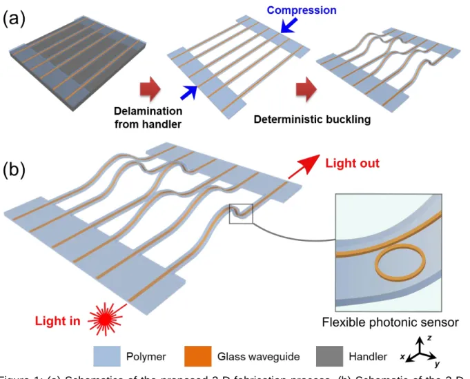
Deterministic 3-D fabrication via buckling. Our fabrication method is illustrated in
Figure 1a. The entire photonic device is first fabricated on top of a rigid handler substrate. It is then delaminated from the handler and deformed into a 3-D structure. The exact shape of the buckled strips is controlled by the thickness profile of the strip and the relative displacement of the two ends during compression. The final structure is illustrated in Figure 1b, with the waveguides and optical components embedded in a polymer cladding structure. The polymer is shaped into strips joining two planar edge platforms with input/output light coupling ports for the devices. For 3-D sensing applications, the design allows arbitrary spatial locations to be accessed by strategically placing waveguide-coupled components (e.g. resonator sensors) on the strips. The in-plane x-y spatial coordinates of a sensing spot are given by the resonator position along the strip, whereas the out-of-plane z-coordinate is defined by the buckle height.
Figure 1: (a) Schematics of the proposed 3-D fabrication process. (b) Schematic of the 3-D device layout.
This fabrication process offers three key advantages. First, it leverages mature planar processing technologies that allow for highly reliable fabrication of optical components.
Second, it is readily scalable to a large number of sensing channels, simply by changing the dimensions of the device (strip width, strip spacing, device overall width, etc.) without compromising the quality and throughput of fabrication. Third, it enables construction of 3-D architectures by controlled, deterministic mechanical deformation – much like pop-up books which come in a planar form and are then deformed into the desired 3-D objects.
For this fabrication method to be deterministic, we need to be able to control the final shape of the buckles such that optical components can be placed at the positions of interest. The buckling of a strip (typically called a "beam" in mechanics) has been solved in a number of specific cases [24]. Our case corresponds to the buckling of a beam with “fixed ends” in which the position and tangent of the ends of the beam are kept constant. The profile of a beam with uniform cross-section buckled under these conditions is given by [25]:
{ 𝑥(𝜙) =1 𝑘[2𝐸(𝜙, 𝑝) − 𝐹(𝜙, 𝑝)] ℎ(𝜙) =2𝑝 𝑘 [1 − cos(𝜙)] , for 0 ≤ 𝜙 ≤ 2𝜋 (1)
where E (resp. F) is the incomplete elliptic integral of the first (resp. second) kind, and p and k are constants determined using the boundary conditions on the initial length of the buckle and its final span (SI-I).
However, in this example the span is the same for all the buckles on a device and all of them end up with the same shape. In order to probe the full 3-D space we need to be able to give different shapes to adjacent buckles. To that end, we modulate the cross-section of the strips by varying their thickness, to create new buckling profiles. The thickness is simply controlled by the number and pattern of top polymer cladding layers on the strips. By applying an additional layer on some areas of the strips but not others, the cross-section and thus the moment of the inertia of the beam vary along its length (Figure SI-2a). The buckled strip shape in this case can also be solved analytically and the solution is presented in SI-I.
This added degree of freedom allows for many more buckle geometries. We show in the next section that fabricated devices with beams made of two segments of different thicknesses agree well with the theoretically predicted shapes. Any more complicated cases, with three or more segments of two or more thicknesses, can be solved and fabricated in a similar way.
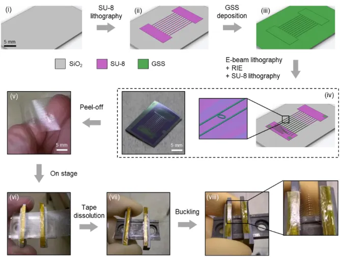
Fabrication and packaging. As mentioned previously, our approach for the
fabrication of our 3-D device was to first fabricate a planar device using well-established 2-D fabrication techniques and then transform it into the target 3-dimensional geometry. The fabrication route is presented in Figure 2. An important feature of this route is that the core material of the waveguides is deposited and processed directly on its polymer cladding. We chose a chalcogenide glass of the composition Ge23Sb7S70 (GSS, with a refractive index of
2.22 at 1550 nm) since it possesses properties important to our target application of a sensing platform notably for biological materials: it is transparent in the near-infrared, has been shown to be non-toxic and resistant to oxidation, and has previously been used to fabricate low-loss devices with a diverse range of applications including flexible photonics [26–29]. SU-8 was used as the polymeric substrate as it meets all the requirements for the encapsulation material: it has good chemical resistance notably to hydrofluoric acid (HF) which is used in a key step of our process as detailed below, is optically transparent at 1550 nm, is known to be biocompatible, is easy to process via photolithography, and is available in a wide range of viscosity allowing for deposition of many different thicknesses (from hundreds of nanometers to hundreds of microns) via spin-coating.
Figure 2: Overall fabrication process flow of the 3-D integrated photonics devices.
Particular care is needed to release the device from its handler substrate (step (v) of Figure 2) while preserving the integrity of the device. A distinguishing feature of our device lies in its patterned structure versus other demonstrations of flexible integrated photonics based on an intact continuous film spanning the entire substrate area [30,31]. Here, the perforated membrane structure is mechanically vulnerable in a free-standing state and therefore we developed a release process using water-soluble tape as a sacrificial supporting substrate [8] before transferring the sample to the precision motion stage for buckling. After transfer, the device lays flat on the stage. It is buckled by bringing the two ends closer together by a controlled distance (step (viii) of Figure 2) and takes on its final 3-D geometry (Figure SI-2b). Figure 3 compares the predicted buckle geometries from Equation (1) and (SI-6), (SI-7) to the experimentally obtained shapes, showing good agreement between the results. This process ensures high fabrication yield of the devices. Further details about the process flow can be found in the Methods section.
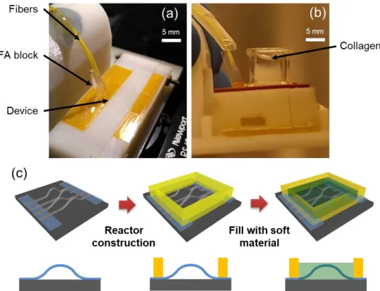
Finally, to provide an easy-to-use, rugged, and reliable platform that readily interfaces with applications involving 3-D photonics, the buckled devices were integrated with an optical fiber array (FA) (Figure 4a). After permanently bonding of the FA to the device using an UV-curable epoxy, no optical alignment setup is required anymore to operate the device, and the devices can be remotely interrogated through the fiber cable connection. This is a critical advantage for many biological and biomechanical sensing applications, where the sensors often need to be deployed in a controlled environment (e.g. inside an incubator or a reactor). FAs also represent a scalable coupling scheme, allowing (time-)multiplexed interrogation of many photonic devices. By combining the packaged devices with spectrally and spatially multiplexed resonators [32], the interrogation scheme can be applied to monitoring a 3-D distributed sensor array containing a large number of individual sensing elements.
Figure 3: Comparison of the fabricated buckle shapes (full lines) with the theoretical predictions (dashed lines). Inset: Picture of the fabricated buckles.
We further demonstrated that the fiber-packaged 3-D sensor array can be embedded inside a soft, biologically-derived material. Figure 4c illustrates the process to integrate the sensor with a cell-laden collagen hydrogel, and Figure 4b shows a photo of the embedded device. The approach enables in-situ, read-time monitoring of various physical and chemical parameters in a 3-D tissue model [33].
Figure 4: (a) Buckled device with bonded 16-channel fiber array. On the left, a stress-relieving structure is used to increase the robustness of the packaged device. (b) Packaged device integrated in collagen. (c) Schematic integration process flow of the 3-D sensor with a material of interest.
Mechanical sensing. As its fabrication relies on planar processing, our platform can
leverage all the functionalities available in the toolbox of standard integrated photonics. Optical resonators have notably been used in a wide spectrum of physical and chemical sensing applications such as label-free protein sensing [34,35], small molecule spectroscopy [36], ultrasound detection [37], or pH and humidity monitoring [38]. Our platform therefore enables multifunctional sensing and mapping in the 3-D space. A promising application of the platform is 3-D mechanical sensing in tissue models. Measuring stress or strain in soft tissues is critical to the understanding of processes such as cell migration and differentiation, yet current methods either do not provide 3-D information [39,40], or are either limited in their spatial extent [41,42], or require complex post-processing [43,44]. Therefore, here we further demonstrate the use of our platform for mechanical sensing. Optical measurements enable strain, or equivalently stress, monitoring through strain-optical coupling in resonator devices [30,45,46]. It has been shown that resonant cavity optical sensors can detect extremely small strains below 0.01% when capitalizing on high-quality resonances [30].
To achieve the target high sensitivity, the stress-induced resonant peak shift must be quantified and isolated from other interfering effects which also result in resonance drift, in particular temperature-dependent wavelength shift (TDWS) due to the thermal-optic effect and thermal expansion of the resonator materials. The TDWS in our resonator devices was measured to be 72 pm/°C [47]. The thermally induced resonance drift is thus much larger than our resonant wavelength measurement accuracy (below 1 pm [48]) even with small temperature fluctuations. We account for the TDWS by placing a second, "temperature-tracking" resonator along each bus waveguide in the flat edge platform of the device that does not undergo deformation. This second resonator only responds to temperature changes in the environment and is used as a reference to nullify TDWS, with the assumption that the temperature is uniform in the space between the strain-sensing and reference resonators (Equation SI-10). To validate this approach, both sets of resonators (Figure SI-3) were measured without any mechanical constraint applied. As shown in Figure 5a, a linear relationship is indeed observed between the resonant wavelengths of the sensing resonator and of the temperature-tracking resonator. This method therefore enables accurate correction for noise caused by temperature fluctuations.
We then quantified the strain response of our sensors by mechanically deforming the individual strips (inset of Figure 5b). The measurement protocols are described in SI-III. The measured resonance shift Δ𝜆 is plotted against the local strain at the resonator (Figure 5b), showing a linear dependence as expected for small deformations [30], with a slope of 3.2 nm/%. This value applies to all resonators with a similar geometry and a similar set of materials. In that respect, it is notably independent of the exact buckle shape and of the position of the resonator with respect to the neutral axis, as both these contributions are accounted for in the value of the strain at the resonator's location. The data further indicate strain measurement accuracy down to 0.01%, suggesting that the embedded photonic sensor platform can be used for sensitive 3-D strain mapping in soft materials (with modulus down to 300 Pa).
Figure 5: (a) Resonant wavelength of the sensing resonator as a function of the peak of the reference (temperature-tracking) resonator, without any stress applied to the device. The error bar on the wavelength readings (both vertically and horizontally) are 1 pm, too small to be seen. The linear fit equation is 𝜆𝑠𝑒𝑛𝑠𝑖𝑛𝑔= 1.2077 ⋅ 𝜆𝑟𝑒𝑓𝑒𝑟𝑒𝑛𝑐𝑒− 326.342 nm . Inset: transmission spectrum of a device over several free-spectral ranges (FSR), with black (resp. red) arrows denoting reference (resp. sensing) peaks, identified through the different FSR of the two resonators. (b) Measured resonance shift as a function of local strain at the resonators. The linear fit equation is Δ𝜆 = 3.2 ⋅ Δ𝜖 − 0.04 nm. Inset: COMSOL model of the system, with a buckle being deformed by a moving block.
Conclusion
In this paper, we present a new method for fabrication and packaging of 3-D integrated photonics with deterministic geometry control. Our fabrication approach benefits from the performances of mature planar processing techniques, offers a controlled, deterministic means by which to position photonic components in 3-D, and is readily scalable to a large volume of devices with unique geometries. Combining this robust manufacturing strategy with
the diverse sensing capabilities offered by integrated photonics will enable a host of applications requiring the complexity of 3-D. Notably, the demonstrated approach will significantly benefit applications where monitoring complex physical/chemical parameter distributions and fluxes is mandatory, for instance in directional electromagnetic wave sensors, flow monitoring in microfluidics, non-destructive structural health monitoring (SHM) in soft materials, as well as synthetic process control in tissue engineering and additive manufacturing. In biological materials, it can also be used to selectively deliver and collect light at/from precise 3-D locations to enable different in-situ light-based diagnosis and stimulation. Overall, the 3-D integrated photonic architecture is well poised to become a multifunctional 3-D sensing and light delivery platform.
Methods
Our device consists of a 2 µm-thick bottom SU-8 layer, a 450 nm-thick GSS layer, and an 8 µm-thick top SU-8 layer (a second 8 µm-thick top layer is used for thickness modulation). Waveguides are 1 µm wide, ring resonators have radii of 30 to 45 µm and a coupling gap of 600 nm. Loaded quality factors of ~30,000 were obtained. Light is coupled into the waveguides using a 250 µm-pitched 16-channel FA of single-mode fibers (SQS Vlaknova Optika) bonded to the device's grating couplers with UV-curable epoxy (Masterbond). The insertion loss per connection is ~10 dB. While not the focus of the present study, the insertion loss can be further reduced with optimized grating coupler designs.
Planar fabrication. Si wafers coated with 300 nm thermal oxide (University Wafer)
were used as substrates. To create the bottom cladding layer, SU-8 2002 (Microchem) was spin-coated, soft baked, patterned using photolithography (MA-4, Süss), hard baked, and developed with propylene glycol monomethyl ether acetate (PGMEA), according to the resist datasheet [49]. Since SU-8 films are prone to stresses [50,51], the more so the thicker they get, we used a temperature ramp for all baking steps, with a hold at 60°C before and after each bake at 95°C. GSS was then deposited onto the entire sample by thermal evaporation. Patterning of the optical components was done using electron-beam lithography followed by dry etching. Prior to electron-beam resist spin-coating, the sample underwent 1 minute of oxygen plasma (100 W, 100 mTorr) to enhance adhesion of the resist, especially on top of the relatively narrow buckles where the step profile would cause poor coverage due to edge effects. 200 nm-thick SU-8 2000.2 (Microchem) was used as the electron-beam resist. During the exposure, we used a height map of the sample to correct for the error in automatic focusing due to the sample surface lying 2 µm above the surface of the substrate, which the laser-based height sensor detects. The SU-8 pattern was then transferred onto the GSS by fluorine-based reactive ion etching (CHF3/Ar gases at 15/35 sccm, 5 mTorr, 300 W ICP power, 60 W
high-frequency power) on an inductively coupled plasma system (Oxford Instruments). SU-8 2005 was then spin-coated, soft baked, exposed, and developed with PGMEA, to create the top cladding layer.
Buckling process. The final planar sample on its substrate was dipped in 12.5%
hydrofluoric acid (HF) for about 5 minutes to undercut the oxide layer and release the device, until it can be visually seen to start lifting off. Water-soluble tape (3M) was then applied onto the sample. Using water-soluble tape alone led to cracks in the device after peel-off because of the low rigidity of the polyvinyl alcohol backing of the tape. We therefore also applied Kapton tape on top of the water-soluble tape to provide structural rigidity during the peeling process. Once on tape and peeled-off from the substrate, the device was placed onto the stage in its flat configuration, with both ends of the stage prepared with double-sided Kapton tape. The entire stage was then dipped in 5% hydrochloric acid (HCl) for a few hours to dilute the tape away. After rinsing in IPA, the flat device was buckled by bringing the two ends of the stage closer together by a controlled distance.
Analytical theory for buckle shapes, temperature-dependent wavelength shift, strain sensing experiment protocols
Acknowledgements
The authors gratefully thank Lionel C Kimerling and Anu Agarwal for providing access to device measurement facilities, and Mark Mondol for technical support with electron-beam lithography. Funding support is provided by the National Science Foundation under awards number 1453218 and 1709212. The authors also acknowledge fabrication facility support by the MIT Microsystems Technology Laboratories and the Harvard University Center for Nanoscale Systems, the latter of which is supported by the National Science Foundation under award 0335765.
References
1. J. H. Cho, M. D. Keung, N. Verellen, L. Lagae, V. V. Moshchalkov, P. Van Dorpe, and D. H. Gracias, "Nanoscale origami for 3D optics," Small 7(14), 1943–1948 (2011). 2. R. J. Wood, "The challenge of manufacturing between macro and micro," Am. Sci.
102(2), 124–131 (2014).
3. D. Bishop, F. Pardo, C. Bolle, R. Giles, and V. Aksyuk, "Silicon micro-machines for fun and profit," J. Low Temp. Phys. 169(5–6), 386–399 (2012).
4. T. G. Leong, C. L. Randall, B. R. Benson, N. Bassik, G. M. Stern, and D. H. Gracias, "Tetherless thermobiochemically actuated microgrippers," Proc. Natl. Acad. Sci.
106(3), 703–708 (2009).
5. K. A. Arpin, A. Mihi, H. T. Johnson, A. J. Baca, J. A. Rogers, J. A. Lewis, and P. V. Braun, "Multidimensional architectures for functional optical devices," Adv. Mater.
22(10), 1084–1101 (2010).
6. T. Ergin, N. Stenger, P. Brenner, J. B. Pendry, and M. Wegener, "Three-Dimensional Invisibility Cloak at Optical Wavelengths," Science (80-. ). 328(5976), 337–339 (2010). 7. K. Suzuki, K. Kitano, K. Ishizaki, and S. Noda, "Three-dimensional photonic crystals
created by single-step multi-directional plasma etching.," Opt. Express 22(14), 17099– 106 (2014).
8. L. Li, H. Lin, S. Qiao, Y.-Z. Huang, J.-Y. Li, J. Michon, T. Gu, C. Alosno-Ramos, L. Vivien, A. Yadav, K. Richardson, N. Lu, and J. Hu, "Monolithically integrated stretchable photonics," Light Sci. Appl. 7(2), 17138 (2018).
9. J. Missinne, N. Teigell Benéitez, A. Lamberti, G. Chiesura, G. Luyckx, M. A. Mattelin, W. Van Paepegem, and G. Van Steenberge, "Thin and Flexible Polymer Photonic Sensor Foils for Monitoring Composite Structures," Adv. Eng. Mater. 20(6), 1701127 (2018).
10. W. Gao, S. Emaminejad, H. Y. Y. Nyein, S. Challa, K. Chen, A. Peck, H. M. Fahad, H. Ota, H. Shiraki, D. Kiriya, D. H. Lien, G. A. Brooks, R. W. Davis, and A. Javey, "Fully integrated wearable sensor arrays for multiplexed in situ perspiration analysis," Nature
529(7587), 509–514 (2016).
11. Z. Bao and X. Chen, "Flexible and Stretchable Devices," Adv. Mater. 28(22), 4177– 4179 (2016).
12. N. Lu, C. Lu, S. Yang, and J. Rogers, "Highly Sensitive Skin-Mountable Strain Gauges Based Entirely on Elastomers," Adv. Funct. Mater. 22(19), 4044–4050 (2012).
13. T. Gissibl, S. Thiele, A. Herkommer, and H. Giessen, "Two-photon direct laser writing of ultracompact multi-lens objectives," Nat. Photonics 10(8), 554–560 (2016).
14. J. T. Muth, D. M. Vogt, R. L. Truby, Y. Mengüç, D. B. Kolesky, R. J. Wood, and J. A. Lewis, "Embedded 3D printing of strain sensors within highly stretchable elastomers.," Adv. Mater. 26(36), 6307–12 (2014).
15. S. Xu, Z. Yan, K.-I. Jang, W. Huang, H. Fu, J. Kim, Z. Wei, M. Flavin, J. McCracken, R. Wang, A. Badea, Y. Liu, D. Xiao, G. Zhou, J. Lee, H. U. Chung, H. Cheng, W. Ren, A. Banks, X. Li, U. Paik, R. G. Nuzzo, Y. Huang, Y. Zhang, and J. A. Rogers,
"Assembly of micro/nanomaterials into complex, three-dimensional architectures by compressive buckling," Science (80-. ). 347(6218), 154–159 (2015).
16. Z. Yan, F. Zhang, J. Wang, F. Liu, X. Guo, K. Nan, Q. Lin, M. Gao, D. Xiao, Y. Shi, Y. Qiu, H. Luan, J. H. Kim, Y. Wang, H. Luo, M. Han, Y. Huang, Y. Zhang, and J. A. Rogers, "Controlled Mechanical Buckling for Origami-Inspired Construction of 3D Microstructures in Advanced Materials," Adv. Funct. Mater. 26(16), 2629–2639 (2016).
17. D. A. Lauffenburger and A. F. Horwitz, "Cell Migration: A Physically Integrated Molecular Process," Cell 84(3), 359–369 (1996).
18. R. Sunyer, V. Conte, J. Escribano, A. Elosegui-Artola, A. Labernadie, L. Valon, D. Navajas, J. M. García-Aznar, J. J. Muñoz, P. Roca-Cusachs, and X. Trepat,
"Collective cell durotaxis emerges from long-range intercellular force transmission," Science (80-. ). 353(6304), 1157–1161 (2016).
19. D. A. Lee, M. M. Knight, J. J. Campbell, and D. L. Bader, "Stem cell mechanobiology.," J. Cell. Biochem. 112(1), 1–9 (2011).
20. J. J. Tomasek, G. Gabbiani, B. Hinz, C. Chaponnier, and R. A. Brown, "Myofibroblasts and mechano: Regulation of connective tissue remodelling," Nat. Rev. Mol. Cell Biol.
3(5), 349–363 (2002).
21. W. J. Polacheck and C. S. Chen, "Measuring cell-generated forces: A guide to the available tools," Nat. Methods 13(5), 415–423 (2016).
22. V. W. Wong, M. T. Longaker, and G. C. Gurtner, "Soft tissue mechanotransduction in wound healing and fibrosis.," Semin. Cell Dev. Biol. 23(9), 981–6 (2012).
23. G. Cheng, J. Tse, R. K. Jain, and L. L. Munn, "Micro-environmental mechanical stress controls tumor spheroid size and morphology by suppressing proliferation and
inducing apoptosis in cancer cells.," PLoS One 4(2), e4632 (2009). 24. S. Timoshenko, Theory of Elastic Stability, 2nd ed. (McGraw-Hill, 1961).
25. T. Hauck, W. H. Müller, and I. Schmadlak, "Nonlinear buckling analysis of vertical wafer probe technology," Microsyst. Technol. 16(11), 1909–1920 (2010).
26. Q. Du, Y. Huang, J. Li, D. Kita, J. Michon, H. Lin, L. Li, S. Novak, K. Richardson, W. Zhang, and J. Hu, "Low-loss photonic device in Ge–Sb–S chalcogenide glass," Opt. Lett. 41(13), 3090 (2016).
27. H. Lin, Y. Song, Y. Huang, D. Kita, S. Deckoff-Jones, K. Wang, L. Li, J. Li, H. Zheng, Z. Luo, H. Wang, S. Novak, A. Yadav, C.-C. Huang, R.-J. Shiue, D. Englund, T. Gu, D. Hewak, K. Richardson, J. Kong, and J. Hu, "Chalcogenide glass-on-graphene photonics," Nat. Photonics 11(12), 798–805 (2017).
28. L. Li, H. Lin, Y. Huang, R.-J. Shiue, A. Yadav, J. Li, J. Michon, D. Englund, K. Richardson, T. Gu, and J. Hu, "High-performance flexible waveguide-integrated photodetectors," Optica 5(1), 44 (2018).
29. Q. Du, C. Wang, Y. Zhang, Y. Zhang, T. Fakhrul, W. Zhang, C. Gonçalves, C. Blanco, K. Richardson, L. Deng, C. A. Ross, L. Bi, and J. Hu, "Monolithic On-chip Magneto-optical Isolator with 3 dB Insertion Loss and 40 dB Isolation Ratio," ACS Photonics
5(12), 5010–5016 (2018).
30. L. Li, H. Lin, S. Qiao, Y. Zou, S. Danto, K. Richardson, J. D. Musgraves, N. Lu, and J. Hu, "Integrated flexible chalcogenide glass photonic devices," Nat. Photonics 8(8), 643–649 (2014).
31. L. Li, P. Zhang, W.-M. Wang, H. Lin, A. B. Zerdoum, S. J. Geiger, Y. Liu, N. Xiao, Y. Zou, O. Ogbuu, Q. Du, X. Jia, J. Li, and J. Hu, "Foldable and Cytocompatible Sol-gel TiO2 Photonics.," Sci. Rep. 5, 13832 (2015).
32. S. Mandal and D. Erickson, "Nanoscale optofluidic sensor arrays," Opt. Express
16(3), 1623 (2008).
33. S. J. Geiger, J. Michon, L. Li, J. Hu, and X. Jia, "Modeling 3-D Photonic Sensor Arrays for Stiffness Gradient Detection in Perfusion-Limited Cardiac Graft Tissue Models," Prep. (n.d.).
34. A. Ksendzov and Y. Lin, "Integrated optics ring-resonator sensors for protein detection," Opt. Lett. 30(24), 3344 (2005).
35. A. Yalcin, K. C. Popat, J. C. Aldridge, T. A. Desai, J. Hryniewicz, N. Chbouki, B. E. Little, V. Van, D. Gill, M. Anthes-Washburn, M. S. Unlu, and B. B. Goldberg, "Optical sensing of biomolecules using microring resonators," IEEE J. Sel. Top. Quantum Electron. 12(1), 148–155 (2006).
36. A. Nitkowski, L. Chen, and M. Lipson, "Cavity-enhanced on-chip absorption spectroscopy using microring resonators," Opt. Express 16(16), 11930 (2008). 37. C. Chao, S. Ashkenazi, S. Huang, M. O’Donnell, and L. Guo, "High-frequency
ultrasound sensors using polymer microring resonators," IEEE Trans. Ultrason. Ferroelectr. Freq. Control 54(5), 957–965 (2007).
38. B. Bhola, P. Nosovitskiy, H. Mahalingam, and W. H. Steier, "Sol-Gel-Based Integrated Optical Microring Resonator Humidity Sensor," IEEE Sens. J. 9(7), 740–747 (2009).
39. S. V. Plotnikov, B. Sabass, U. S. Schwarz, and C. M. Waterman, "High-Resolution Traction Force Microscopy," in Methods in Cell Biology (2014), 123, pp. 367–394. 40. C. Grashoff, B. D. Hoffman, M. D. Brenner, R. Zhou, M. Parsons, M. T. Yang, M. A.
McLean, S. G. Sligar, C. S. Chen, T. Ha, and M. A. Schwartz, "Measuring mechanical tension across vinculin reveals regulation of focal adhesion dynamics," Nature
466(7303), 263–266 (2010).
41. C. Franck, S. Hong, S. A. Maskarinec, D. A. Tirrell, and G. Ravichandran, "Three-dimensional Full-field Measurements of Large Deformations in Soft Materials Using Confocal Microscopy and Digital Volume Correlation," Exp. Mech. 47(3), 427–438 (2007).
42. J. Toyjanova, E. Bar-Kochba, C. López-Fagundo, J. Reichner, D. Hoffman-Kim, and C. Franck, "High resolution, large deformation 3D traction force microscopy," PLoS One 9(4), e90976 (2014).
43. H. Xu, S. F. Othman, and R. L. Magin, "Monitoring Tissue Engineering Using Magnetic Resonance Imaging," J. Biosci. Bioeng. 106(6), 515–527 (2008).
44. A. Buljac, C. Jailin, A. Mendoza, J. Neggers, T. Taillandier-Thomas, A. Bouterf, B. Smaniotto, F. Hild, and S. Roux, "Digital Volume Correlation: Review of Progress and Challenges," Exp. Mech. 58(5), 661–708 (2018).
45. W. J. Westerveld, J. Pozo, P. J. Harmsma, R. Schmits, E. Tabak, T. C. van den Dool, S. M. Leinders, K. W. A. van Dongen, H. P. Urbach, and M. Yousefi, "Characterization of a photonic strain sensor in silicon-on-insulator technology.," Opt. Lett. 37(4), 479– 81 (2012).
46. L. Fan, L. T. Varghese, Y. Xuan, J. Wang, B. Niu, and M. Qi, "Direct fabrication of silicon photonic devices on a flexible platform and its application for strain sensing.," Opt. Express 20(18), 20564–75 (2012).
47. S. Geiger, Q. Du, B. Huang, M. Y. Shalaginov, J. Michon, H. Lin, T. Gu, A. Yadav, K. A. Richardson, X. Jia, and J. Hu, "Understanding aging in chalcogenide glass thin films using precision resonant cavity refractometry," Opt. Mater. Express 9(5), 2252 (2019).
48. J. Hu, X. Sun, A. Agarwal, and L. C. Kimerling, "Design guidelines for optical resonator biochemical sensors," J. Opt. Soc. Am. B 26(5), 1032 (2009). 49. "SU-8 Datasheet,"
http://microchem.com/pdf/SU-82000DataSheet2000_5thru2015Ver4.pdf.
50. H. Lorenz, M. Laudon, and P. Renaud, "Mechanical characterization of a new high-aspect-ratio near UV-photoresist," Microelectron. Eng. 41–42, 371–374 (1998). 51. S. Keller, G. Blagoi, M. Lillemose, D. Haefliger, and A. Boisen, "Processing of thin
SU-8 films," J. Micromechanics Microengineering 1SU-8(12), 125020 (200SU-8).
52. G.-D. Kim, H.-S. Lee, C.-H. Park, S.-S. Lee, B. T. Lim, H. K. Bae, and W.-G. Lee, "Silicon photonic temperature sensor employing a ring resonator manufactured using a standard CMOS process," Opt. Express 18(21), 22215 (2010).
53. S. Katz and S. Givli, "The post-buckling behavior of a beam constrained by springy walls," J. Mech. Phys. Solids 78, 443–466 (2015).
54. T. Y. Wang, C. G. Koh, and C. Y. Liaw, "Post-buckling analysis of planar elastica using a hybrid numerical strategy," Comput. Struct. 88(11–12), 785–795 (2010). 55. A. Pocheau and B. Roman, "Uniqueness of solutions for constrained Elastica," Phys.
D Nonlinear Phenom. 192(3–4), 161–186 (2004).
56. B. Roman and A. Pocheau, "Postbuckling of bilaterally constrained rectangular thin plates," J. Mech. Phys. Solids 50(11), 2379–2401 (2002).
Supporting Information
A 3-D integrated photonics platform with deterministic geometry
control
Jérôme Michon1, Sarah Geiger1,2, Lan Li3,4, Claudia Gonçalves5, Hongtao Lin6, Kathleen Richardson5, Xinqiao Jia2, Juejun Hu1
1Department of Materials Science and Engineering, MIT, Cambridge MA, USA 2Department of Biological Engineering, University of Delaware, Newark DE, USA 3Key Laboratory of 3D Micro/Nano Fabrication and Characterization of Zhejiang Province,
School of Engineering, Westlake University, Hangzhou, China
4Institute of Advanced Technology, Westlake Institute for Advanced Study, Hangzhou, China 5College of Optics & Photonics, University of Central Florida, Orlando FL, USA
6College of Information Science and Electronic Engineering, Zhejiang University, Zhejiang,
SI-I: Analytical theory for predicting the shape of buckles with non-uniform
cross-sections
Here we show that, given parameters under control such as the buckle's total length and its span, we can predict the shape of the buckle. The assumptions made throughout the derivations are as follows:
• The material of the beam is homogeneous and isotropic. Previous work in our group has shown that the presence of the glass could be neglected [16, 29].
• The compressive load on the beam is axial only. • The beam is free from initial stress.
• The weight of the beam (and any other lateral load) is neglected. • The stress never exceeds the yield strain.
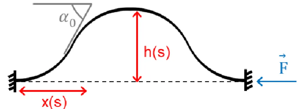
The following notations are also used (Figure SI-1): - x: horizontal coordinate of points of the beam
- h: vertical coordinate of points of the beam (i.e. height profile of the beam) - 𝛼0: angle of deflection of the buckle
- s: arc length along the buckle - Ltot: total length of the beam
- L: length of the beam along the x-direction after buckling - E: Young's modulus of the beam material
- I: moment of inertia of the beam (for a given cross-section). In particular, for a beam with rectangular cross-section of width w and thickness t, its moment of inertia with respect to its neutral axis is 𝐼 = 𝑤ℎ3/3.
- F: load applied at the end of the beam
Figure SI-1: Schematic side-view of a uniform cross-section buckle. 1. Uniform cross-section beam buckling
Using a large-deformation approach, the curvature is given by 𝑑𝛼/𝑑𝑠, with 𝛼 the angle of deflection of the beam at each position. The differential equation governing the behavior of the beam is thus [25]:
𝐸𝐼𝑑 2𝛼 𝑑𝑠2+ 𝐹
𝑑ℎ
𝑑𝑠 = 0 (SI-1)
The value of F is unknown but will be determined later on. The profile of the buckle is then given by: { 𝑥(𝜙) =1 𝑘[2𝐸(𝜙, 𝑝) − 𝐹(𝜙, 𝑝)] ℎ(𝜙) =2𝑝 𝑘 [1 − cos(𝜙)] , for 0 ≤ 𝜙 ≤ 2𝜋 (SI-2)
where 𝑘2= 𝐹/𝐸𝐼, 𝑝 = sin(𝛼0
2) with 𝛼0 the angle of deflection at the inflection point, and 𝐸(𝜙, 𝑝) and 𝐹(𝜙, 𝑝) are the incomplete elliptic integrals of the second and first kind, respectively. The boundary conditions used to obtain these expressions are:
{𝑥(0) = ℎ(0) = 0
ℎ′(0) = ℎ′(𝐿) = 0 (SI-3)
The values of k and p0 are found by considering two additional conditions: the total length 𝐿𝑡𝑜𝑡 of the device is conserved upon buckling, and the position 𝑥(2𝜋) = 𝐿 of the right edge of the buckle is known. The total length of the buckle can be calculated as:
𝐿𝑡𝑜𝑡= ∫ √𝑥′(𝑡)2+ ℎ′(𝑡)2𝑑𝑡 = 4𝐾(𝑝) 𝑘 2𝜋 0 (SI-4) where K(p) is the complete elliptic integral of the first kind.
The conditions on k and p0 are therefore: { 𝐿 =1 𝑘[2𝐸(2𝜋, 𝑝) − 𝐹(2𝜋, 𝑝)] 𝐿𝑡𝑜𝑡= 4𝐾(𝑝) 𝑘 (SI-5) Because elliptic integrals have no analytical expression, this system needs to be solved numerically.
2. Piecewise uniform cross-section
We consider here the case of a beam made of two segments of different thicknesses. This treatment can easily be extended to three or more segments. The two segments are described by their moment of inertia I1 and I2, and their length l1 and l2 = Ltot – l1. Solving Equation 9 for each segment yields two profiles of the form of Equation 10, for 0 ≤ 𝜙 ≤ Φ and Φ ≤ 𝜙 ≤ 2π, with Φ the (unknown yet) parameter giving the junction's position. We can write the horizontal position of the beam as:
𝑥(𝜙) = { 1 𝑘1 [2𝐸(𝜙, 𝑝1) − 𝐹(𝜙, 𝑝1)], for 0 ≤ 𝜙 ≤ Φ 1 𝑘1 [2𝐸(Φ, 𝑝1) − 𝐹(Φ, 𝑝1)] + 1 𝑘2 [2[𝐸(𝜙, 𝑝2) − 𝐸(Φ, 𝑝2)] − [𝐹(𝜙, 𝑝2) − 𝐹(Φ, 𝑝2)]] (SI-6) for Φ ≤ 𝜙 ≤ 2π
Its vertical position is:
ℎ(𝜙) = { 2𝑝1 𝑘1 [1 − cos(𝜙)], for 0 ≤ 𝜙 ≤ Φ 2𝑝1 𝑘1 [1 − cos(Φ)] +2𝑝2 𝑘2 [cos (Φ) − cos(𝜙)] , for Φ ≤ 𝜙 ≤ 2π (SI-7) In both cases we used the continuity at Φ.
We have 5 parameters (𝑝1, 𝑘1, 𝑝2, 𝑘2, Φ), we need 5 equations. These are given by the
lengths of each segment, the boundary conditions at each end of the buckle, and the relation between 𝑘1 and 𝑘2 due to the force balance at the junction.
{ 𝑙1= 1 𝑘1 𝐹(Φ, 𝑝1) 𝑙2= 1/𝑘2[𝐾(𝑝2) − 𝐹(Φ, 𝑝2)] 𝐿 = 1 𝑘1 [2𝐸(Φ, 𝑝1) − 𝐹(Φ, 𝑝1)] + 1 𝑘2 [2[4𝐸(𝑝2) − 𝐸(Φ, 𝑝2)] − [4𝐾(𝑝2) − 𝐹(Φ, 𝑝2)]] 0 =2𝑝1 𝑘1 [1 − cos(Φ)] +2𝑝2 𝑘2 [cos (Φ) − 1] 𝑘1 𝑘2 = (𝑡2 𝑡1 ) 3 (SI-8)
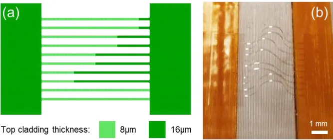
Figure SI-2: (a) Mask for the top cladding. (b) Sample fabricated using this mask, whose buckles were used as the experimental shapes in Figure 3.
SI-II: Temperature-dependent wavelength shift correction
The equation giving the temperature-dependent wavelength shift (TDWS) is [52]: Δ𝜆𝑇𝐷𝑊𝑆= 𝛼 𝑛𝑒𝑓𝑓 𝑛𝑔 𝜆Δ𝑇 + 1 𝑛𝑔 𝜕𝑛𝑒𝑓𝑓 𝜕𝑇 𝜆Δ𝑇 = 𝛼𝑛𝑒𝑓𝑓+ 𝜎 𝑛𝑔 𝜆Δ𝑇 = 𝛽Δ𝑇 (SI-9)
with T the temperature, 𝜆 the wavelength, 𝛼 the thermal expansion coefficient, 𝜎 = 𝜕𝑛𝑒𝑓𝑓⁄𝜕𝑇, and 𝛽 = (𝛼𝑛𝑒𝑓𝑓+ 𝜎)𝜆 𝑛⁄ 𝑔. Over a small range of temperature, we can neglect the dependence of the coupling coefficient 𝛽 on temperature (through the wavelength, the effective index 𝑛𝑒𝑓𝑓, and the group index 𝑛𝑔), leading to a linear relationship between TDWS and temperature. This equation can be applied to both sensing and reference resonators, with different values for beta as the local geometry varies between the temperature-tracking resonator on the flat "island" and the resonator in the bent buckle. The two equations can then be combined to yield a linear relation linking the TDWS of the two resonators:
Δ𝜆𝑇𝐷𝑊𝑆,𝑏𝑢𝑐𝑘𝑙𝑒 =
𝛽𝑏𝑢𝑐𝑘𝑙𝑒 𝛽𝑇−𝑡𝑟𝑎𝑐𝑘𝑖𝑛𝑔
Δ𝜆𝑇𝐷𝑊𝑆,𝑇−𝑡𝑟𝑎𝑐𝑘𝑖𝑛𝑔 (SI-10)
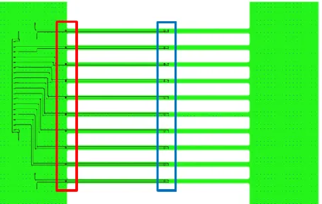
Figure SI-3: 2-D layout (blue) of the photonic device on top of the base SU-8 pattern (green). The temperature-tracking rings are boxed in red and the stress-sensing rings are boxed in blue.
SI-III: Strain sensing experiment protocols
We use external force to controllably deform the strips and quantify the strain-optical coupling behavior of our sensors. Specifically, the buckled strips are subjected to linear displacement of a rigid boundary (practically speaking, a block of stiff material). The experimental setup was used to acquire optical data, while finite element models where used to calculate the local strains.
In order to get repeatable and precise deformation, we used a piezoelectric actuator (TRA25CC, Newport) to control the vertical position of the block. The initial position was chosen such that the block would barely not touch the top of the buckle. It was then lowered in steps of 0.1 or 0.2 mm. After each block movement, an optical spectrum was acquired. The block was lowered down to 1.3 mm below its original position, then brought back up in the same increments, and several such rounds of lowering and raising were performed. The acquired spectra were analyzed to extract the peak shift of the resonators. The experiment was performed in an open laboratory without ambient temperature control. Therefore, the measured peak shift included both deformation-induced and temperature-induced contributions. The spectra acquired at the initial position, when no deformation is applied to the buckle, were thus used to calibrate the relationship between the temperature-dependent wavelength shifts of the temperature-tracking resonator and the pressure-tracking resonator. This relationship was then applied to the other spectra to calculate the temperature-induced peak drift, subtract it from the total measured peak shift, and thereby isolate the deformation-induced resonance change.
The configuration used, with the buckle constrained between the stage and an upper block, is commonly referred to as "the constrained elastica" – a beam under buckling constrained in the vertical direction. Its treatment has been the subject of a number of numerical and analytical studies [53–56]. Yet no analytical solution was found in a general case. We therefore implement numerical simulations to study this problem. We used the finite element modeling (FEM) software COMSOL to simulate the behavior of the system under the applied constraints. Given the symmetries of the problem, with the block moving only vertically and the buckle standing in a plane, a 2-D model can be used. The results of the simulations include the displacement field and final curvature of the buckle. We then compared the final curvature to the curvature in the initial state to calculate the change in curvature along the buckle due to the deformation. Finally, knowing the position of the sensor along the buckle, and using the relationship between curvature and strain, we calculated the change in stress as a function of the magnitude of the deformation (in this case, the height change of the upper block).