HAL Id: hal-03091793
https://hal.archives-ouvertes.fr/hal-03091793
Submitted on 7 Jan 2021
HAL is a multi-disciplinary open access
archive for the deposit and dissemination of
sci-entific research documents, whether they are
pub-lished or not. The documents may come from
teaching and research institutions in France or
abroad, or from public or private research centers.
L’archive ouverte pluridisciplinaire HAL, est
destinée au dépôt et à la diffusion de documents
scientifiques de niveau recherche, publiés ou non,
émanant des établissements d’enseignement et de
recherche français ou étrangers, des laboratoires
publics ou privés.
Double side nanostructuring of microcantilever sensors
with TiO2-NTs as a route to enhance their sensitivity
Guillaume Thomas, Geoffrey Gerer, Laurent Schlur, Fabien Schnell, Thomas
Cottineau, Valérie Keller, Denis Spitzer
To cite this version:
Guillaume Thomas, Geoffrey Gerer, Laurent Schlur, Fabien Schnell, Thomas Cottineau, et al.. Double
side nanostructuring of microcantilever sensors with TiO2-NTs as a route to enhance their sensitivity.
Nanoscale, Royal Society of Chemistry, 2020, 12 (25), pp.13338-13345. �10.1039/D0NR01596B�.
�hal-03091793�
rsc.li/nanoscale
Nanoscale
rsc.li/nanoscaleISSN 2040-3372
PAPER Shuping Xu, Chongyang Liang et al. Organelle-targeting surface-enhanced Raman scattering (SERS) nanosensors for subcellular pH sensing
Volume 10 Number 4 28 January 2018 Pages 1549-2172
Nanoscale
This is an Accepted Manuscript, which has been through the
Royal Society of Chemistry peer review process and has been
accepted for publication.
Accepted Manuscripts are published online shortly after acceptance,
before technical editing, formatting and proof reading. Using this free
service, authors can make their results available to the community, in
citable form, before we publish the edited article. We will replace this
Accepted Manuscript with the edited and formatted Advance Article as
soon as it is available.
You can find more information about Accepted Manuscripts in the
Information for Authors
.
Please note that technical editing may introduce minor changes to the
text and/or graphics, which may alter content. The journal’s standard
Terms & Conditions
and the
Ethical guidelines
still apply. In no event
shall the Royal Society of Chemistry be held responsible for any errors
or omissions in this Accepted Manuscript or any consequences arising
from the use of any information it contains.
Accepted Manuscript
This article can be cited before page numbers have been issued, to do this please use: G. Thomas, G. Gerer, L. Schlur, F. Schnell, T. Cottineau, V. Keller and D. Spitzer, Nanoscale, 2020, DOI:
COMMUNICATION
Please do not adjust margins
Please do not adjust margins
Received 00th January 20xx, Accepted 00th January 20xx DOI: 10.1039/x0xx00000x
Double side nanostructuring of microcantilever sensor with
TiO
2-NTs as a route to enhance their sensitivity
Guillaume Thomas,
aGeoffrey Gerer,
a,bLaurent Schlur,
aFabien Schnell,
aThomas Cottineau,
bValérie Keller
band Denis Spitzer
a *We reported a new strategy to enhance the sensing performances of a commercial microcantilever with optical readout in dynamic mode for the vapor detection of organophosphorous coumpounds (OPs). In order to increase significantly the surface area accessible to the molecules in vapor phase, we nanostructured both sides of the microcantilever with ordered, open and vertically oriented amorphous titanium dioxide nanotubes (TiO2-NTs) in one step by
an anodization method. However, due to the agressive conditions of anodization synthesis it remains a real challenge to nanostructure both sides of the microcantilever. Consequently, we developped and optimized a protocol of synthesis to overcome these harsh conditions which can lead to the total destruction of the silicon microcantilever. Moreover, this protocol was also elaborated in order to maintain a good reflection of the laser beam on one side of the cantilever towards the position sensitive photodiode and limit the light diffusion by the NTs film. The first results related to the detection of dimethyl methylphosphonate (DMMP) showed that TiO2 and the nanostructuring on both sides
of the microcantilever with NTs improved indeed the response of the sensor to vapors compared to a microcantilever nanostructured on only one side. The dimensions and morphology of NTs guaranteed the access of molecule to the surface of NTs. This approach showed promising perspectives to enhance the sensing performances of microcantilevers.
Introduction
Potential exposure to chemical warfare agents (CWAs) from terrorist organizations or military groups is real.1–3 They have
been used during the 2013 Syrian civil war and more recently, in 2017-2018, against civilians in Syria, Malaysia and United Kingdom.4 Among these agents, organophosphorous
compounds (OPs) such as tabun (GA), sarin (GB) or VX can be used as weapons of mass destruction and are toxic molecules.1,3
This potential threat leads to develop sensors with high selectivity and sensitivity. The next generation of sensors must be fast, sensitive, selective, portable and inexpensive. However, it remains a challenge to satisfy all the requirements in a single sensor. Different sensors based on mass spectrometry,5
colorimetry,6 photonic crystals,7 surface acoustic wave8,9 have
been proposed but they often require bulky instrumentations and high costs. Microgravimetric sensors and more particularly microcantilevers are a good candidate and showed promising results due to their low cost, their ease of handle, their reversibility and their good sensitivity.10–16 To date, different
strategies have been explored to improve their effectiveness about the detection of OPs. The first strategy consists mostly in functionalizing the microcantilever surface. For example, a self-assembled composite layer of Cu2+/11-mercaptoundecanoic
acid,10 a hyper-branched polymer,12,14 or 78-mer 5’-biotinylated
aptamer have been fixed on the microcantilever surface.13
However, the organic molecules are not stable at high temperatures and over long periods of time. The second strategy to improve molecule capture ability of the microcantilevers consists in enhancing their surface of capture which is originally low.17 It usually achieved by the formation of
a nanostructure on its surface. It has begun since a decade with the synthesis of titanium dioxide nanotubes (TiO2-NTs) on one
side of a microcantilever for the detection of explosives.17–20
Thundat et al. also nanostructured the surface of the microcantilever with a nanoporous TiO2.19 Their
nanostructuring required a two-step anodization and photolithography process for the detection of trace explosives. However, the use of photolithography process is not cost-effective. More recently, Cai et al. developed a metal-organic framework (MOF) of UiO-66 film on a Parylene-C patterned piezoresistive microcantilever in order to increase the active
a.Nanomatériaux pour les Systèmes Sous Sollicitations Extrêmes (NS3E), UMR 3208
ISL/CNRS/UNISTRA, French-German Research Institute of Saint-Louis, 5, rue du Général Cassagnou, 68300 Saint-Louis, France.
b.Institut de Chimie et Procédés pour l’Energie, l’Environnement et la Santé (ICPEES)
UMR 7515 CNRS/Université de Strasbourg, 25 rue Becquerel, 67087 Strasbourg, France.
*Corresponding author: denis.spitzer@isl.eu
† Footnotes relating to the title and/or authors should appear here.
Electronic Supplementary Information (ESI) available: [details of any supplementary information available should be included here]. See DOI: 10.1039/x0xx00000x
Page 1 of 8
Nanoscale
Nanoscale
A
cc
ep
te
d
Ma
n
u
sc
ri
p
t
View Article Online
COMMUNICATION
Journal Name
2 | J. Name., 2012, 00, 1-3 This journal is © The Royal Society of Chemistry 20xx
surface area and the probability of DMMP capture.11 However,
the use of MOFs is limited due to drawbacks such as high fabrication costs, low reversibility, pore modulation or stability.21 Despite the fact that these strategies improve
significantly the sensitivity of the microcantilever, the nanostructures were only limited to one side of the microcantilever. They did not nanostructure the opposite side of the microcantilever may be due to harsh conditions of synthesis17,18 for microcantilevers, important costs19 or
problems of laser beam reflection as reported previously for microcantilevers nanostructured with zinc oxide nanorods.22
Microcantilever with optical readout consists in reflecting a laser beam on a side of the microcantilever towards a position-sensitive detector in order to follow the resonance frequency during sensing experiments in dynamic mode. This technique is expected to result in a better sensitivity than the piezoresistive detection, especially in this mode.17,23 Indeed, local heating can
appear due to flowing current during measurement and piezoresistive layer needed for integration affects the mechanical performance.23
Here, to overcome the cited problems, we report for the first time, a cost-effective and optimized synthesis of ordered and vertically aligned TiO2 nanotubes on both (upper and lower)
sides of a commercial microcantilever with optical readout by anodization. This process has the advantage to (i) not require photolithography process (high costs),19 (ii) to use TiO
2 which is
a material widely employed in photochemical and photoelectrochemical applications24–26, to be easily
synthesize25 and showing a good interaction with simulant of
OPs,20,27,28 (iii) to generate NTs which develop a high surface to
volume ratio, (iv) to reflect the laser beam on the microcantilever and (v) to offer a higher enlargement of the surface area due to the double side nanostructuring compared to the single one. The aim of the double nanostructuring is to increase the surface area of the microcantilever and consequently its sensitivity by enhancing the number of captured molecules. Among the different syntheses of TiO2
-NTs, we chose anodization synthesis. It consists of the anodization of titanium layer for NTs formation. This synthesis has the advantage to be relatively easy on centimeter-sized area, simple, inexpensive and different kind of electrolytes can be used to allow the growth of a wide variety of TiO2-NTs
morphologies and dimensions.17,29 However, it remains a big
challenge to nanostructure both sides of the commercial microcantilever in a one-step anodization without damaging the microcantilever. Indeed, the presence of fluoride in the electrolyte as well as high applied voltage can easily dissolve the microcantilever which is characterized by a small size (few square micrometer area). The microcantilevers must resist to the synthesis conditions in order to preserve their mechanical properties and consequently their high sensitivity. Moreover, the NTs on the microcantilever surface have to reflect the laser beam light used to measure the resonance frequency. This is also a challenge to conserve this property due to the decrease of the reflective index of TiO2 compared to Si and also the
formation of the porous surface coming from NTs which can prevent the laser reflection.
Due to the extreme high toxicity of the nerve agents, simulants as DMMP,2 are preferentially used as model for sensing
experiments. These molecules are less toxic and are characterized by a behavior close to the nerve agents making them good candidates for laboratory experiments.2
Results and discussion
The protocol developed to nanostructure both sides of the microcantilever is presented in Scheme 1: (1) A bare silicon microcantilever (TL-NCL-50 from NanosensorsTM) with a
thickness of 7 ± 1 µm, a length of 225 ± 10 µm, a width of 38 ± 8 µm and a force constant of 21-98 N.m-1 was used as
received. (2) The front side of the microcantilever was coated with a thick layer (layer No.1) of titanium by physical vapor deposition (PVD). The process used here is sputtering. Deposition was done at a pressure of 2 x 10⁻³ mbar under argon
atmosphere at 60 °C and the magnetron power density was 9.66 W.cm2. (3) The previous step was also applied to the back
side of the microcantilever (layer No. 2). The front side (layer No. 1) of the microcantilever was deposited on a gel layer composed of polydimethylsiloxane (PDMS) in order to protect it during titanium deposition. However, the deposition temperature was here fixed at room temperature (23 °C). The deposition parameters were optimized in order to guarantee the growth of TiO2-NTs. (4) Synthesis of vertically aligned
TiO2-NTs on the microcantilevers was done by electrochemical
anodization of the metallic Ti layers. This method has been reported in a previous work30 and modified here in order to
obtain dense, open and oriented TiO2-NTs on both sides
without any damage on microcantilever (e.g. dissolution of silicon). Briefly, the anodization was conducted in a two electrodes cell with the titanium covered microcantilever as working electrode and a platinum foil as counter electrode. The electrolyte was composed of 0.5% (w/w) NH4F and 10.0% H2O
(v/v) in ethylene glycol at 45 °C. The same protocol (except step 2) was applied to the microcantilever nanostructured on one side.
The anodization process is a competition between the electrochemical oxidation of Ti into TiO2 and the dissolution of
the oxide by the fluoride of the electrolyte according to the Eqs. (1) and (2):17,31
Scheme 1 Schematic synthesis of the double side nanostructuring of
microcantilevers with optical readout by TiO2-NTs.
Nanoscale
A
cc
ep
te
d
Ma
n
u
sc
ri
p
t
View Article Online
Journal Name
COMMUNICATION
This journal is © The Royal Society of Chemistry 20xx J. Name., 2013, 00, 1-3 | 3
Please do not adjust margins
Please do not adjust margins
(1) Ti + 2H2O→TiO2+4e―+4H+
(2) TiO2+6F-+4H+→[TiF6]2 ―+2H2O
In the case of thin silicon substrate (7 ± 1 µm), it is crucial to pay attention not to dissolve the silicon with the fluoride of the electrolyte as presented in Fig 1.17 Silicon and silicon dioxide
suffer indeed from dissolution in the fluoride solutions.32,33
Consequently, we used an ethylene glycol based electrolyte having a high viscosity which slows down the diffusion of fluorides and consequently limits the silicon dissolution. Moreover, parameters were specifically adapted to generate the formation and opening of TiO2-NTs while limiting the
dissolution of silicon by fluorides. Electrolyte was composed of 0.5% (w/w) NH4F and 10.0% H2O (v/v) in ethylene glycol at
45 °C. The same protocol (except step 2) was applied to the microcantilever nanostructured on one side.
Scanning electron microscopy (SEM) images of a one and double side nanostructured microcantilever with a potential of anodization of 60 V are presented on Fig.2. We observe the presence of NTs on one side (Fig.2 a) and on both sides (Fig.2.b) of the single and double side nanostructured microcantilever, respectively. This protocol of synthesis allows the nanostructuring on both sides. With these conditions, NTs of the single nanostructured microcantilever have a length of 1240 ± 38 nm, an external diameter of 137 ± 13 nm and an internal diameter of 105 ± 13 nm. Concerning the double side nanostructured microcantilever, NTs have a length of 1854 ± 137 nm, an external diameter of 100 ± 6 nm and an internal diameter of 72 ± 7 nm. Then, we optimized the conditions of synthesis by applying a potential of anodization of 20 V and a time of synthesis of 1800 s in order to increase the surface area of the microcantilevers by reducing the diameter and increasing the length of NTs.
SEM images (top views) after each optimized synthesis step are displayed on Fig.3. The side views of the microcantilever after the synthesis of TiO2-NTs are exposed on Fig.4. As
observed on the Fig.3, bare microcantilever shows a smooth surface. After sputtering deposition, Ti layers are characterized by a slight roughness (Fig.3 b)). The Ti layers are formed of
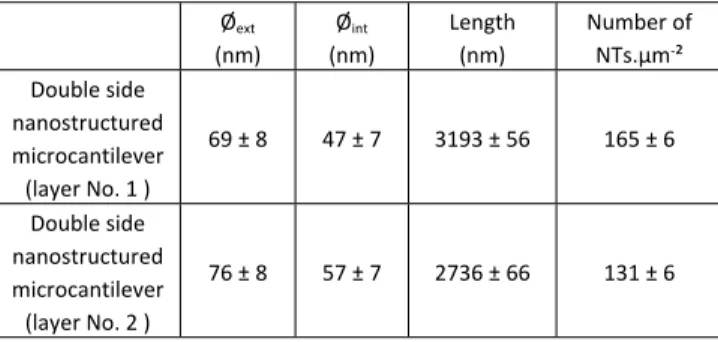
randomly oriented platelet-shaped particles. The thickness of Ti films measured by scanning electron microscopy (SEM) was 2.2 ± 0.1 µm. These Ti layers were then anodized in the optimized conditions (1800 s, 20 V). After anodization, SEM images show ordered and vertically aligned NTs on both surfaces of the microcantilever. Moreover, the top of NTs are completely open. Transmission electron microscopy (TEM) images confirm also the formation of NTs (Fig.5). This opening ensures the access of molecules into the NTs allowing a possible increase of the molecules capture. The layer No. 1 exhibits NTs with a length of 2736 ± 66 nm, an external diameter of 76 ± 8 nm and an internal diameter of 57 ± 7 nm (Table 1 and Fig.3 b). The layer No. 2 exhibits NTs with a length of 3193 ± 56 nm, an external and internal diameter of 69 ± 8 nm and 47 ± 7 nm, respectively (Table 1 and Fig. 3 b)). We reach a density of 131 ± 6 and 165 ± 6 NTs.µm-² (determined by
counting the NTs on SEM images) on the layer No. 1 and No. 2, respectively. NTs are characterized by a high aspect ratio (length to diameter ratio) of 46 and 36 for layer No. 1 and 2, respectively. The orientation and morphology of NTs lead to increase significantly the surface area until a factor of 343 (theoretical value extracted from dimensions of the NTs) for double side nanostructured microcantilever (Table 1). This value is much higher than the result obtained in a previous study with one side nanostructured microcantilever (80).18
We also observe that the length of TiO2-NTs between the
two layers is slightly different. This difference could be explained by the temperature applied during the sputtering
Fig. 1 Optical images of a microcantilever covered by a Ti layer (thickness of
2.2 ± 0.1 µm) a) before anodization and b) after anodization without synthesis optimization (one side of the cantilever was not protected during deposition of Ti layer, potential of anodization and time of synthesis were fixed at 30 V and 1800 s, respectively).
Fig. 2 SEM images of microcantilever covered on a) one side (back side) and b) on both sides by TiO2-NTs. The potential of anodization is fixed at 60 V for single nanostructured microcantilever and double side nanostructured microcantilever. The potential of anodization was fixed at 60 V.
Page 3 of 8
Nanoscale
Nanoscale
A
cc
ep
te
d
Ma
n
u
sc
ri
p
t
View Article Online
COMMUNICATION
Journal Name
4 | J. Name., 2012, 00, 1-3 This journal is © The Royal Society of Chemistry 20xx
deposition of Ti layer (60 °C and 25 °C for layer No. 1 and layer No. 2, respectively). We suppose here that a high temperature modifies Ti layer by increasing the grain size as reported in previous works.34–36 Moreover, this effect lead to reduce the
defect/gap between the grains resulting in denser film as previously reported.35 As observed on Fig.2, the layer No. 2 is
characterized by a more pronounced stacking of platelet-shaped titanium and less dense film than on layer No. 1. This arrangement leads to more grain boundaries and interfaces on Layer No 2. These interfaces may act like passages for the interstitial rapid diffusions of O2- according to the diffusion
theory that may facilitate chemical reaction between Ti4+ and
O2- improving the growth of TiO
2-NTs as observed in a previous
report.37 Moreover, as we used only one counter electrode
during anodization process, the local electric field is consequently different between the two sides of the microcantilever which could lead to modify the dimensions of NTs on both sides. Further experiments are necessary to explain completely the mechanism of reaction during this step.
To determine crystallinity of nanostructures, X-ray diffraction (XRD) was employed (Fig. 6). After sputter deposition on a silicon wafer, we observed the (100), (002), (101) and (102) planes corresponding to the Ti crystal structure (JCPDS: 00-44-1294).38,39 After anodization, we observe that the peaks
corresponding to the Ti crystal structure remain present on the XRD pattern. However, we noticed that their intensity is
reduced indicating the titanium consumption during the anodization. NTs are amorphous because no peaks characteristic of any titanium oxide phase is observed. Additionally, after a thermal treatment of the anodized sample at 450 °C during 4 hours (with a rate of 5 °C/min), we observe three diffraction peaks at 25.4°, 44.5° and 48.2°. The peaks at 25.4° and 48.2° are attributed to (101) and (200) planes of anatase crystalline phase respectively (JCPDS: 01-078-2486).40
The peak at 44.5° is attributed to the diffusion of Si in Ti grain boundaries.41 The remaining peaks correspond to the Si wafer.
To resume, these results confirm that (i) a layer of Ti remains
Fig. 3 SEM images of bare microcantilever, microcantilever covered by a Ti layer and microcantilever covered by TiO2-NTs on both upper (layer No. 2) and lower surfaces (layer No. 1) with a a) large and b) close view. The particles visible on bare microcantilever (b)) are dust particles present on the microcantilever and they were used to adjust the focus on the microcantilever surface.
Fig. 4 SEM images of double side nanostructured cantilever with TiO2-NTs.
Fig. 5 TEM images of TiO2-NTs obtained from nanostructured wafer.
Table 1. Dimensions of TiO2-NTs (length, external (Øext) and internal diameter
(Øint)) and numbers of TiO2-NTs on the double side nanostructured
microcantilevers (layer No. 1 and layer No. 2).
Øext (nm) Øint (nm) Length (nm) Number of NTs.µm-² Double side nanostructured microcantilever (layer No. 1 ) 69 ± 8 47 ± 7 3193 ± 56 165 ± 6 Double side nanostructured microcantilever (layer No. 2 ) 76 ± 8 57 ± 7 2736 ± 66 131 ± 6
Nanoscale
A
cc
ep
te
d
Ma
n
u
sc
ri
p
t
View Article Online
Journal Name
COMMUNICATION
This journal is © The Royal Society of Chemistry 20xx J. Name., 2013, 00, 1-3 | 5
Please do not adjust margins
Please do not adjust margins
between the substrate (Si) and the layer of TiO2-NTs and (ii)
TiO2-NTs are amorphous after anodization.
We have successfully nanostructured both surfaces of the microcantilever with ordered, completely open and vertically oriented TiO2-NTs. The anodization synthesis took place in a
single step. This strategy of patterning on both sides increases highly the surface area. This high surface area coming from intratubular, interstitial channels, external groove and external rounded surfaces of NTs could highly enhance the sensing properties of the next generation of microcantilever.
In order to evaluate the benefits of this nanostructuring strategy, bare microcantilever, microcantilever covered by metallic titanium film and microcantilever nanostructured on its both sides with TiO2-NTs were exposed to DMMP vapor. The
potential of anodization and the synthesis time used to nanostructure the microcantilever were fixed at 20 V and 1800 s. The microcantilever was exposed to 594 ppm of DMMP for 10 minutes at a flow rate of 50 mL.min-1.The DMMP vapors
were generated from an air flow going through a stainless steel bubbler containing a pure solution of DMMP maintained at a temperature of 16 °C. The DMMP concentration was determined by gas chromatography-mass spectrometry with a measured concentration of 594 ppm which was close to the estimated saturated concentration (562 ppm) by using the Antoine equation.42 The adsorption measurements are
illustrated in Fig 7. The three microcantilevers respond to DMMP vapor with a resonance frequency drop just after the injection of DMMP. The frequency shifts are -13, -50, -632 Hz for bare microcantilever, microcantilever with Ti layer and double side nanostructured microcantilever respectively. Despite the presence of the TiO2-NTs, the reflection of the laser
beam on the TiO2-NTs surface towards the position sensitive
photodiode is conserved. The measurement of the resonance frequency shift is thus ensured. Uncovered and Ti covered microcantilevers respond very slightly to DMMP. However, the
cantilever covered by a Ti layer shows a higher response (-50 Hz) compared to the uncovered cantilever (-13 Hz). This effect could be attributed to the increase of the surface area due to presence of the platelet-shaped titanium structures on the surface of the microcantilever as observed in Fig. 3. The observed difference can also be due the fact that a native titanium oxide layer formed at air exposure has been probably generated on the surface of titanium layer and which could be more reactive to DMMP than silicon. Previous studies showed that TiO2 has indeed a good reactivity to DMMP.20,27,43,44 The
initial uptake of DMMP on TiO2 surface involves hydrogen
bonds between the P=O group and hydroxyl groups of the oxide surface.27,44,45 When both sides of the microcantilever are
nanostructured with two dense layers of TiO2-NTs, a high
response is observed with a shift of -632 Hz (f0 = 166.105 kHz).
The response is multiplied by a factor of 48 compared to the uncovered microcantilever. This result confirms that the nanostructuring offers better response than bare microcantilever. Moreover, it confirms also that TiO2 is a
material having a positive response to DMMP while the dimensions of NTs ensure an access of DMMP molecules on their surface. After 10 min of exposure to DMMP, microcantilevers are again exposed to air. As observed, for all tested microcantilevers, the resonance frequency shift decreases, indicating that DMMP molecules are progressively desorbed from the surface (Fig. 4). For the double side nanostructured microcantilever, we can underline that the response of the cantilever to DMMP vapor is very fast with a response time inferior to 2 s and an initial rate of 527 Hz.s-1. 90%
of the threshold is reached in only 14 s. After 100 s, the frequency of the microcantilever reached an equilibrium value (-632 Hz). However, the desorption process takes more time
Fig.7 Resonance frequency shift of the bare microcantilever (Si), microcantilever
covered by a Ti layer and double side nanostructured microcantilever with TiO2-NTs. The
microcantilevers were exposed to 594 ppm of DMMP for 10 min. Double side nanostructured cantilever was synthesized with a potential of anodization of 20 V and a synthesis time of 1800 s.
Fig. 6 XRD patterns of silicon wafer before (green) and after deposition of a titanium layer
(blue), TiO2-NTs before (black) and after thermal treatment at 450 °C (red). TiO2-NTs are
obtained by anodization.
Page 5 of 8
Nanoscale
Nanoscale
A
cc
ep
te
d
Ma
n
u
sc
ri
p
t
View Article Online
COMMUNICATION
Journal Name
6 | J. Name., 2012, 00, 1-3 This journal is © The Royal Society of Chemistry 20xx
than adsorption with a response time inferior to 2 s. 90% of the return to the baseline is achieved in 125 s. A time superior to 600 s is necessary to observe a return of the baseline. The comparison of adsorption and desorption times shows that desorption is much slower process than adsorption. It can be explained by the fact that DMMP could be trapped in pores which results in a slow release process. Further studies are necessary to determine in details the mechanisms of DMMP adsorption and desorption on TiO2-NTs. According to the
mechanism of vapor permeation, the response of the nanostructured microcantilever to DMMP can be considered by three steps: i.e. adsorption, diffusion, and desorption process. First, the frequency changes sharply (initial rate of 527 Hz.s-1)
when the double side nanostructured mirocantilever is introduced with vapors (DMMP), which results from surface adsorption effect. Then, the frequency shifts very slowly and the frequency nearly not change because of bulk diffusion effect between sensitive sensor material (TiO2) and vapor. This
interaction process is called a dynamic process where adsorption and desorption processes occur simultaneously. When the number of adsorbed vapor molecules is equal to the number of desorbed vapor molecules, the frequency change reaches a stable value. After flushing the air, a rapid change of kinetic response will occur due to desorption of DMMP vapor which is a surface and bulk effect.
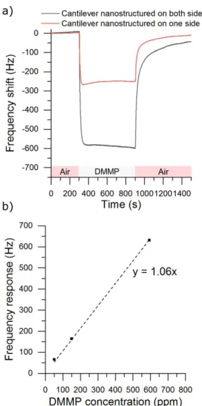
Additionally, we also exposed the double side nanostructured microcantilever to 50 and 147 ppm of DMMP (Fig. 8-b)). We observed respectively a frequency response of 66 and 164 Hz. The estimated limit of detection (LOD) is 2.8 ppm and the sensitivity is about 1.06 Hz.ppm-1.
The response to DMMP of a double nanostructured microcantilever is also compared to a microcantilever nanostructured on only one side, as illustrated in Fig. 8. The potential of anodization and the synthesis times were respectively fixed at 15 V and 1800 s for both cantilevers. We notice a response of -247 Hz and -583 Hz, for the single and double side nanostructured sensor respectively. As observed on Fig.8, the double side nanostructuring improves significantly the response of the sensor by a factor of 2.3, compared to the microcantilever nanostructured on only one side. This result highlights here the benefit of the dual nanostructuring over the single nanostructuring by increasing the surface area and offering consequently a higher amount of interaction sites on the surface of the sensor.
As a result, TiO2 material offers a good reactivity towards
DMMP molecules. TiO2-NTs and double side nanostructuring
offer a high opportunity to increase easily and highly the sensitivity of the microcantilever by enhancing capabilities to adsorb the molecules due to the large surface area enhancement. We are currently developing different organic molecules in order to functionalize the nanostructure surface. The aim is to increase the sensitivity of the sensor as well as the selectivity to organophosphorous compounds.
Conclusion
In summary, we have developed a fast route for enhancing commercial microcantilever response to DMMP vapor. First, we have covered both sides (upper and lower) of a silicon microcantilever with a titanium layer by physical vapor deposition and then, we nanostructured the microcantilever with TiO2-NTs by anodization. Anodization of both surfaces has
been realized in a one-step process. Through an optimized protocol of titanium deposition and anodization synthesis, we have successfully kept sufficient reflectivity by maintaining surface properties and morphology of the microcantilever as well as the initial structure and morphology of the microcantilever despite the harsh conditions of titanium anodization for silicon. Additionally, we have homogenously nanostructured the sensor with open, dense and vertically oriented amorphous TiO2-NTs. The morphology of NTs ensures
a good accessibility of the DMMP molecules on the nanostructures surface. Moreover, the NTs morphology and the double side nanostructuring offers a high enhancement of the surface area which should increase the sensor sensitivity.
Fig. 8 a) Resonance frequency shift of a microcantilever nanostructured on one and both
sides with TiO2-NTs. The microcantilevers were exposed to 594 ppm of DMMP for 10 min.
Nanostructured microcantilevers were synthesized with a potential of anodization of 15 V and a synthesis time of 1800 s. b) Frequency responses of the double side microcantilever. Double side nanostructured cantilever was synthesized with a potential of anodization of 20 V and a synthesis time of 1800 s.
Nanoscale
A
cc
ep
te
d
Ma
n
u
sc
ri
p
t
View Article Online
Journal Name
COMMUNICATION
This journal is © The Royal Society of Chemistry 20xx J. Name., 2013, 00, 1-3 | 7
Please do not adjust margins
Please do not adjust margins
Indeed, NTs allowed to capture more molecules on the surface of the microcantilever and double side nanostructured microcantilever showed an enhancement of the sensor response by a factor of two compared to the single nanostructured microcantilever. In addition, TiO2 is a good
candidate to detect OPs. Double side nanostructured microcantilever showed a fast response and a good recovery. By taking advantage of the high surface area of the double side nanostructuring, further development will be conducted in order to develop a more sensitive and selective sensor to OPs.
Conflicts of interest
There are no conflicts to declare.
References
1 M. Kloske and Z. Witkiewicz, Chemosphere, 2019, 221, 672–682. 2 Y. J. Jang, K. Kim, O. G. Tsay, D. A. Atwood and D. G. Churchill,
Chem. Rev., 2015, 115, PR1–PR76.
3 R. C. Gupta, Handbook of toxicology of chemical warfare agents, Academic Press, 2015.
4 M. Lane, D. Carter, J. D. Pescrille, Y. Aracava, W. P. Fawcett, G. W. Basinger, E. F. R. Pereira and E. X. Albuquerque, bioRxiv, 2020, 2020.02.03.932798.
5 Y. Seto, M. Kanamori-Kataoka, K. Tsuge, I. Ohsawa, K. Iura, T. Itoi, H. Sekiguchi, K. Matsushita, S. Yamashiro, Y. Sano and others, Anal. Chem., 2013, 85, 2659–2666.
6 S. Qian and H. Lin, Anal. Chem., 2015, 87, 5395–5400. 7 J. D. Kittle, B. P. Fisher, A. J. Esparza, A. M. Morey and S. T.
Iacono, ACS Omega, 2017, 2, 8301–8307.
8 B. Minot, C. Frenois, S. Besnard, J. Bordet, N. Martins and F. Pereira, Procedia Eng., 2016, 168, 423–427.
9 X. Du, Z. Ying, Y. Jiang, Z. Liu, T. Yang and G. Xie, Sens. Actuators
B Chem., 2008, 134, 409–413.
10 G. Zuo, X. Li, P. Li, T. Yang, Y. Wang, Z. Cheng and S. Feng, Anal.
Chim. Acta, 2006, 580, 123–127.
11 S. Cai, W. Li, P. Xu, X. Xia, H. Yu, S. Zhang and X. Li, Analyst, 2019,
144, 3729–3735.
12 Y. Liu, P. Xu, H. Yu, G. Zuo, Z. Cheng, D.-W. Lee and X. Li, J.
Mater. Chem., 2012, 22, 18004–18009.
13 R. Zhao, Y. Wen and X. Yu, in 2015 Transducers-2015 18th
International Conference on Solid-State Sensors, Actuators and Microsystems (TRANSDUCERS), IEEE, 2015, pp. 1487–1490.
14 S. Guo, P. Xu, H. Yu, X. Li and Z. Cheng, Sens. Actuators B Chem., 2015, 209, 943–950.
15 S. Guo, P. Xu, H. Yu, Z. Cheng and X. Li, Anal. Chim. Acta, 2015,
863, 49–58.
16 M. Chaudhary and A. Gupta, Def. Sci. J., 2009, 59, 634–641. 17 T. Cottineau, S. N. Pronkin, M. Acosta, C. Mény, D. Spitzer and V.
Keller, Sens. Actuators B Chem., 2013, 182, 489–497. 18 D. Spitzer, T. Cottineau, N. Piazzon, S. Josset, F. Schnell, S. N.
Pronkin, E. R. Savinova and V. Keller, Angew. Chem. Int. Ed., 2012, 51, 5334–5338.
19 D. Lee, S. Kim, S. Jeon and T. Thundat, Anal. Chem., 2014, 86, 5077–5082.
20 U. Biapo, A. Ghisolfi, G. Gerer, D. Spitzer, V. Keller and T. Cottineau, ACS Appl. Mater. Interfaces, 2019, 11, 35122–35131.
21 K. Vikrant, V. Kumar, K.-H. Kim and D. Kukkar, J. Mater. Chem. A, 2017, 5, 22877–22896.
22 L. Schlur, J. R. Calado and D. Spitzer, R. Soc. Open Sci., 2018, 5, 180510.
23 H. Debéda and I. Dufour, in Advanced Nanomaterials for
Inexpensive Gas Microsensors, Elsevier, 2020, pp. 161–188.
24 T. Cottineau, N. Béalu, P.-A. Gross, S. N. Pronkin, N. Keller, E. R. Savinova and V. Keller, J. Mater. Chem. A, 2013, 1, 2151–2160. 25 B. Yin, Q. Qian, Z. Xiong, H. Jiang, Y. Lin and D. Feng,
Nanotechnology, 2019, 30, 155702.
26 M. Lampimäki, S. Schreiber, V. Zelenay, A. e elov , M. Birrer, S. Axnanda, B. Mao, Z. Liu, H. Bluhm and M. Ammann, J. Phys.
Chem. C, 2015, 119, 7076–7085.
27 D. A. Panayotov and J. R. Morris, Langmuir, 2009, 25, 3652– 3658.
28 D. A. Panayotov and J. R. Morris, J. Phys. Chem. C, 2009, 113, 15684–15691.
29 Y. Fu and A. Mo, Nanoscale Res. Lett., 2018, 13, 187. 30 I. Gonzalez-Valls, A. Mirloup, T. Le Bahers, N. Keller, T.
Cottineau, P. Sautet and V. Keller, RSC Adv., 2016, 6, 91529– 91540.
31 P. Roy, S. Berger and P. Schmuki, Angew. Chem. Int. Ed., 2011,
50, 2904–2939.
32 J. H. Ouyang, X. S. Zhao, T. Li and D. C. Zhang, J. Appl. Phys., 2003, 93, 4315–4320.
33 Y. A. Simonov, A. Kritskii, V. Rychkov and V. Tomashov, Russ. J.
Non-Ferr. Met., 2010, 51, 320–323.
34 M. Einollahzadeh-Samadi, R. S. Dariani and M. Abdi, J. Mater.
Res., 2015, 30, 3093–3103.
35 K. N. Chappanda, Y. R. Smith, L. W. Rieth, P. Tathireddy, M. Misra and S. K. Mohanty, IEEE Trans. Nanotechnol., 2014, 14, 18–25.
36 C.-P. Liu and H.-G. Yang, Mater. Chem. Phys., 2004, 86, 370–374. 37 L. Zhang and Y. Han, Nanotechnology, 2009, 21, 055602. 38 I. Jauberteau, R. Mayet, J. Cornette, D. Mangin, A. Bessaudou, P.
Carles, J. Jauberteau and A. Passelergue, Coatings, 2017, 7, 23. 39 D. Constantin, C. Moura, D. Munteanu and L. Cunha, J.
Optoelectron. Adv. Mater., 2012, 14, 964.
40 N. Raddaha, L. Cordero-Arias, S. Cabanas-Polo, S. Virtanen, J. Roether and A. Boccaccini, Materials, 2014, 7, 1814–1829. 41 O. Chaix-Pluchery, B. Chenevier, I. Matko, J.-P. Sénateur and F.
La Via, J. Appl. Phys., 2004, 96, 361–368.
42 A. B. Butrow, J. H. Buchanan and D. E. Tevault, J. Chem. Eng.
Data, 2009, 54, 1876–1883.
43 J. A. Moss, S. H. Szczepankiewicz, E. Park and M. R. Hoffmann, J.
Phys. Chem. B, 2005, 109, 19779–19785.
44 C. N. Rusu and J. T. Yates, J. Phys. Chem. B, 2000, 104, 12292– 12298.
45 V. Bermudez, J. Phys. Chem. C, 2011, 115, 6741–6747.
Page 7 of 8
Nanoscale
Nanoscale
A
cc
ep
te
d
Ma
n
u
sc
ri
p
t
View Article Online
Table of content
Double side nanostructured microcantilever with ordered, aligned and open TiO2 nanotubes
Nanoscale
A
cc
ep
te
d
Ma
n
u
sc
ri
p
t
View Article Online