Design of a Photonic Crystal Planar Luneburg Lens
for Optical Beam Steering
by Samuel Kim B.A. Physics Harvard University, 2015
Submitted to the
Department of Electrical Engineering and Computer Science in Partial Fulfillment of the Requirements for the Degree of Master of Science in Electrical Engineering and Computer Science
at the
Massachusetts Institute of Technology June 2019
@2019
Massachusetts Institute of Technology. All rights reservedSignature redacted
Signature of the author:Department of Electrical Engineering and Computer Science
I A April 26, 2019
Signature redacted
Certified by: Marin Soljaei6 Professor of Physics Thesis SupervisorSignature redacted
Accepted by: L/ V Leslie A. Kolodziejski Professor of Electrical Engineering and Computer Science MASSACHUSETTS INSTITUTE Chair, Department Committee on Graduate StudentsOF TECHNOLOGY
77 Massachusetts Avenue (Cmhridge, MA 02139
http://ibraries.mit.edu/ask
DISCLAIMER NOTICE
Due to the condition of the original material, there are unavoidable flaws in this reproduction. We have made every effort possible to provide you with the best copy available.
Thank you.
The images contained in this document are of the best quality available.
Design of a Photonic Crystal Planar Luneburg Lens for Optical
Beam Steering
by Samuel Kim
Submitted to the Department of Electrical Engineering and Computer Science on April 26, 2019 in Partial Fulfillment of the
Requirements for the Degree of
Master of Science in Electrical Engineering and Computer Science
ABSTRACT
Optical beam steering has numerous applications including light detection and ranging (LIDAR) for three-dimensional (3D) sensing, free space communications, additive manufac-turing, and remote sensing. In particular, there is an increasing demand for LIDAR in a variety of applications including autonomous vehicles, unammaned aerial vehicles (UAVs), robotics, and remote sensing. Ideal solutions are small in size, weight, and power consump-tion (SWaP) while maintaining long range, high resoluconsump-tion, and large field of view (FOV).
Here I present a design for a planar Luneburg lens for use in a silicon photonics optical beam steering device fabricated using CMOS-compatible techniques. The gradient index of the lens is achieved using a photonic crystal consisting of amorphous silicon patterned with a triangular lattice of holes layered on top of silicon nitride. Multiple waveguides can be placed along the focal circle of the lens and the lens is designed to collimate the beam from the waveguides. Through full-wave simulations, the lens is shown to be diffraction-limited with a beamwidth of 0.55' for a lens with radius R = 100 um. The lens is also studied for
robustness to fabrication variations. The lens would allow a solid-state on-chip optical beam steering device with a FOV of 1600 with no off-axis aberrations.
Thesis Supervisor: Marin Soljaeid Title: Professor of Physics
Acknowledgements
I would like to first acknowledge my research supervisor, Professor Marin Solja3id, for his continuous support of my research. He has allowed me to work as independently as possible while also keeping his door open to me to talk about anything ranging from tackling specific technical challenges in my work to approaching my career goals. He is an inspiring scientist and advisor who pushes me to be successful.
I would also like to thank everyone with whom I have had the pleasure to work with on this project. Professor Steven Johnson has taught me a tremendous amount on the beauty of photonic crystals, and he and Professor George Barbastathis have provided insightful comments on how to approach this project during its early stages. I am grateful for my entire research group for their support both technically and personally, and for providing a collaborative and fun environment to work in. In particular, I would like to thank Josue L6pez and Jamison Sloan who have been working on related projects before I started this work. They got me up to speed and worked closely with me on pushing this project forward. Finally, I am grateful for my family and friends including my blockmates from college and my friends here at MIT. They have all supported me throughout the years and pushed me to pursue my passions and go as far as possible. Without them I would not have pursued this path.
Contents
1 Introduction 13
2 Luneburg Lens Theory 17
3 Lens Implementation 23
3.1 Materials and Fabrication . . . . 24
3.2 Photonic Crystals . . . . 24
3.3 Photonic Crystal Lens . . . . 30
3.4 Other Photonic Crystals . . . . 31
4 Methods for Lens Simulation 35 5 Results 39 5.1 Lens Perform ance . . . . 39
5.2 Robustness to Fabrication . . . . 48
List of Figures
1.1 Architecture .of lens-based chip-scale LIDAR system. Figure from [30]
@2017
M IT . . . .. . . . 15 2.1 Ray tracing of the Luneburg lens in normalized coordinates such that theradius of the lens is R = 1. The Luneburg lens focuses two spheres concentric
with the lens onto each other. In this example, the conjugate focal spheres have radii ro oc and r1 = s such that rays emanating from a point source
are collim ated by the lens. . . . . 17 2.2 Luneburg lens normalized refractive index as a function of normalized radius.
(a) Original Luneburg formulation for fixed ro = oc and various r1 = s. (b)
Generalized formulation with an outer shell of constant index nc, ro = 00, and r1 = 2. n= 1 is equivalent to the original Luneburg formulation. Note that setting n, > 1 increases the maximum refractive index required but also decreases the range of the refractive index required. . . . . 19 3.1 (a) 3D Schematic of the photonic crystal consisting of a layer of a-Si with a
triangular lattice of holes sitting on a layer of SiN. The a-Si and SiN layers have thicknesses t and 200 nm, respectively. (b) Top view of the photonic crystal. The lattice has periodicity a and the holes have diameter d. . . . . . 25
3.2 Reciprocal lattice of the triangular lattice. The dotted line represents the Brillouin zone and the shaded triangle represents the irreducible Brillouin zone. The corners of the irreducible Brillouin zone are denoted as the IF, K,
and M points. . . . . 26 3.3 Wavelength and thickness dependence of refractive index of a-Si layer. . . . . 27 3.4 Dependence of the refractive index of the photonic crystal as a function of t
an d d . . . . 28 3.5 Anisotropy of the photonic crystal as measured by the ratio of the effective
indices at the K and M points in (a) 3D and (b) 2D. . . . . 28 3.6 Validity of the effective index approximation of the photonic crystal as
mea-sured by the ratio of phase to group index in (a) 3D and (b) 2D. . . . . 29 3.7 (a) Luneburg lens index profile for s = 2.8 (blue) and the effective index
achieved by the photonic crystal (orange). (b) Photonic crystal d as a function of lens radius to achieve the Luneburg lens index profile. . . . . 30 3.8 Photonic crystal implementation of the Luneburg lens with R = 10 Jm. Black
represents the a-SI slab while white represents the SiN slab. (a) s = 2.8. The index profile is shown in Figure 3.7. Note the region in the center of the lens where d = 0 pm and it is a solid a-Si slab. (b) s = 5. The dotted line
represents the desired perimeter of the lens, but the desired the index is too low to achieve with the photonic crystal and so the lens region is truncated. 31 3.9 (a) Cross and (b) 3-stepped cross shapes for a triangular lattice. The crosses
are inscribed in a regular hexagon (inner dotted line) which is concentric with and oriented the same way as the hexagonal unit cell that it lies in (outer dotted line). The dimensions of the crosses are determined by a single param eter, d. . . . . 32
3.10 (a) Ratio nross/nhole where ncross and nhole are the refractive indices of the cross and circular hole-based photonic crystals, respectively. (b) Ratio ncross/nhole where neroes and nhole are the refractive indices of the 3-stepped cross and cir-cular hole-based photonic crystals, respectively. . . . . 32 3.11 Anisotropy of the photonic crystal as illustrated by the ratio nM/nK for (a)
the cross photonic crystal and (b) the 3-stepped cross photonic crystal. . . . 33
4.1 (a) Permittivity profile of the 2D simulation in MEEP. Black is a-Si, grey is SiN, and white is SiO2. (b) Resulting magnetic field, H, of the MEEP
sim ulation . . . . 36 4.2 Farfield plots for a lens with radius R = 30 lim. (a) Polar plot of the farfield
in the SiN slab. (b) Farfield corrected for air and zoomed into the main lobe. 37 5.1 Simulation of the lens (gray) with a plane wave sent in from the right so
that we can see focusing. (a) H, profile (red and blue). (b) Time-averaged magnetic field energy density, to H 12/2 (orange). . . . . 40
5.2 Results of sending in a plane wave into the lens and measuring the focused field. (a) Error in the focal length measured by the location of the maximum field. (b) Resolution criterion of the focused field as measured by the distance from the maximum field to the first minimum, 6, and the analytical solution for the Rayleigh diffraction limit. The points for R = 50 jim and R = 100 pm are overlayed on each other and thus cannot be seen separately. . . . . 40 5.3 H, (red and blue) overlayed on the permittivity profile (greyscale) of a
simu-lation of a dipole source and an ideal lens with s = 2 and R = 25 pm. .... 42 5.4 Far field FWHM of the collimated beam using an ideal lens and both a dipole
source and waveguide (WG) source. The dotted line is the analytical FWHM assuming a uniformly illuminated aperture, which results in a sine function pattern in the farfield. . . . . 42
5.5 Behavior of a waveguide mode traveling from a waveguide into a waveguide slab. (a) H, (b) Streamlines of the time-averaged Poynting vector, S. Only vectors above an aribtrary threshold are plotted to better visualize the beam in the lab. The point at which the waveguide meets the slab waveguide is at x = 0 . . . . . 4 3 5.6 The predicted focal point at each yi along several slices in xi. . . . . 44 5.7 Effect of photonic crystal periodicity. Lens simulation with (a) a = 300 nm,
(b) 400 nm , and (c) 500 nm . . . . 45 5.8 Far field of photonic crystal lens and idealized lens for R = 30 im. . . . . 46 5,9 (a) Far field of the photonic crystal lens for various radii. (b) FWHM of the
photonic crystal lens, idealized lens, and idealized lens illuminated by a dipole source for various lens radii. For reference the analytical FWHM of an Airy disk profile and a Gaussian beam are also plotted. . . . . 46 5.10 Far field of photonic crystal lens as a function of lens rotation. . . . . 47 5.11 Measuring robustness to fabricated a-Si thickness, where the designed a-Si
thickness is t = 30 nm . . . . 48 5.12 Measuring robustness to fabricated a-Si thickness, where the designed a-Si
thickness is t = 30 nm and there are 64 ports. . . . . 49 5.13 Robustness of the lens performance to the hole size by applying Gaussian
noise 6
d ~ A(pd, Jd) to the hold size as d' = d +E. This is measured fractional
change of the FWHM with respect to the unperturbed lens as a function of (a) Ad for 0d = 10 (the dotted line represent the case where Ad = and o = 0
and (b) Ud for Ad = 0 . . . . 49 5.14 Robustness of the lens performance to the hole location by applying Gaussian
noise 6, ~ JV(,, ar) to the coordinates of each hole as x' = x + c, and
y y + cr. Set y, = 0. This is measured as the fractional change of the
Chapter 1
Introduction
Optical beam steering consists of actively controlling the direction of a laser beam over a range of angles. It has numerous applications [1, 2] including light detection and ranging (LIDAR) for mapping and navigation [3], free-space optical communications, projection [4], and additive manufacturing.
In LIDAR, a three-dimensional (3D) map of an environment or remote object is con-structed by sending out a pulsed laser light at various angles and measuring the reflected pulse. Analagous to radar, LIDAR uses the return time and wavelength of the reflected light to compute the distance and relative velocity at each direction in space. The number of re-ceived photons can also be used to measure reflectance of the surface. LIDAR has long been used for creating detailed 3D maps of terrains for construction [5], mining [6], agriculture [7], archaeology [8], environmental science (e.g., flood mapping, forestry, vegetation map-ping, erosion of sandy beaches) [9], and many more applications. More recently, commercial interest in more portable LIDAR has increased dramatically for applications in self-driving vehicles [10], autonomous robots [7], and unmanned aerial vehicles (UAVs) [11].
Free-space optical communications encodes information in a modulated light pulse to wirelessly send information to a remote receiver and is useful in scenarios where physical connections are impractical such as communications with vehicles, aircraft, or spacecraft. It
is also attractive because the bandwidth of optical communications is orders of magnitude greater than that of radio-frequency (RF) communications. While optical communications typically uses LEDs as the light source, there is large interested in using a steered laser beam to improve efficiency, range, and security [12].
With increasing use of robots, vehicles, and drones, there is also increasing interest in LIDAR or free-space optical communications devices that are suited for these platforms. These applications requires low weight, size, power, and cost (SWAP-C) while maintaining performance metrics such as range, resolution, scan rate, and field of view (FOV). Because these platforms are moving and often undergo harsh conditions, they require high reliability and robustness. Additionally, the increasing commercial interest in LIDAR requires future solutions to be more scalable. All of these factors drive towards solid-state on-chip solutions for optical beam steering [13].
Current commercial solutions for optical beam steering typically use lasers that are mounted on a rotating stage or stationary lasers that are redirected using a moving mir-ror, lens, prism, or diffraction grating. However, the moving parts make these solutions bulky, heavy, power-hungry, difficult to mass manufacture, and unreliable. There have been a number of solid-state solutions for optical beam steering that do not use moving parts, although they all currently face tradeoffs in the aforementioned factors. A tunable spatial light modulator (SLM) using liquid crystals as the tunable element can be used as a passive optical phased array (OPA) where the liquid crystal controls the phase of a reflected or trans-mitted beam at each point in space, thus tuning the direction of the reflected or transtrans-mitted beam [1, 13, 14, 15, 16]. Metasurfaces that are actively controlled through electronically tunable materials such as vanadium oxide can be used in a similar manner to redirect the phase front of a transmitted beam through the metasurface [17]. Microelectromechanical systems (MEMS) optical beam steering typically consists of actuated mirrors fabricated on a silicon chip to steer a beam [18, 19, 20, 21, 22]. MEMS offers greater reliability and smaller SWAP-C characteristics than macro-mechanical solutions because of the on-chip integration,
but it is not truly solid-state because of the moving parts and so it still suffers from sensitiv-ity to vibrations. Active OPAs use an array of optical antennas that are actively controlled in phase to steer the outgoing beam [2, 3, 4, 23, 24, 25, 26, 27]. Active OPAs are attractive because of their fully integrated and solid-state design but still suffer from limited FOV due to sidelobes and have high complexity of phase controls. Another solution uses discrete switching between different waveguides combined with a 3D lens for beam steering, although this is not on-chip and would require an extra alignment step in manufacturing [28, 29].
Edge Fiber MZI Switch Waveguide Slab-Waveguide Aplanatic 1D Coupling Matrix Feed Interface Lens Grating
Si02 Silicon Nitride Amorphous Silicon
Figure 1.1: Architecture of lens-based chip-scale LIDAR system. Figure from [30]
@2017
MIT.An alternative architecture for chip-scale LIDAR has been proposed [30] and experimen-tally demonstrated [31] to address the shortcomings of other optical beam steering solutions, and a schematic of the architecture is shown in Figure 1.1. In this architecture, a tunable laser source centered at 1550 nm couples into an on-chip waveguide made of silicon nitride (SiN) encapsulated in silicon dioxide (SiO2). The waveguide feeds into a switch matrix
com-posed of Mach-Zehnder interferometers that can route the signal into one of N waveguide ports. The waveguide ports feed into a SiN slab at different azimuthal (in-plane) angles, where an aplanatic lens consisting of amorphous silicon (a-Si) layered on top of SiN colli-mates the beam from each port. Thus, by switching the port that the signal routes through, this architecture can change the in-plane angle of the collimated beam. Finally, a grating consisting of a-Si rulings on top of SiN scatters the beam out of plane. By tuning the wave-length of the source, one can change the out-of-plane angle, thus enabling two-dimensional
(2D) beam steering.
This architecture has much lower power consumption than OPAs due to the need to control only O(log2 N) switches at a time as opposed to M phase tuners for OPAs. It also
has the advantage of reduced thermal management, simpler control systems, and robustness to environmental factors. However, this architecture has an azimuthal FOV of 20' due to off-axis aberrations of the lens, which limits its applications. There are a number of wide angle lens designs with FOV up to 1900, but these suffer from asymmetric behavior of the entrance pupil and aperture size as one moves off-axis [32] which would reduce performance off-axis and make the following grating more difficult to design.
Here, I propose a new lens design based on the Luneburg lens that has a theoretical FOV of 3600. The Luneburg lens is a spherically symmetric lens that maps two spheres onto each other. It is a gradient-index (GRIN) lens in that the index of refraction smoothly varies across the lens. Here, a photonic crystal is used to realize the gradient index of the lens. The lens is designed within the constraints of CMOS-compatible fabrication techniques. Full-wave electromagnetic simulations are used to predict the behavior of the lens as well as study the robustness of the lens to variations in fabrication.
Chapter 2
Luneburg Lens Theory
Focal sphere
Parallel rays Luneburg Lens
S
Point source
Figure 2.1: Ray tracing of the Luneburg lens in normalized coordinates such that the radius of the lens is R = 1. The Luneburg lens focuses two spheres concentric with the lens onto each other. In this example, the conjugate focal spheres have radii ro = 00 and r1 = s such
that rays emanating from a point source are collimated by the lens.
The Luneburg lens is a spherically symmetric gradient-index lens that focuses two spheres concentric with the lens onto each other, where the focal spheres have radii equal or greater than that of the lens as shown in Figure 2.1 [33]. For example, in the case where the object sphere has radius ro = oo and image sphere has radius r1 = R where R is the radius of the
lens, then parallel rays coming from any direction focus onto a point on the surface of the lens opposite of the incoming rays. Vice versa, rays emanating from a point source on the
surface of the lens will be collimated by the lens on the opposite side of the lens from the point source. As opposed to traditional lenses that use a single material with a constant index of refraction, the index of refraction of the Luneburg lens n(r) varies smoothly as a function of the radial position r < R inside the lens, thus making it a gradient-index lens. The gradient index causes the rays to bend inside the lens, enabling focusing.
For simplicity in this discussion, assume that n(r) is normalized by the index of the surrounding medium, no, and that radial quantities (r, ro, and ri) are normalized to R. For the case where ro - so and r1 = 1, Luneburg presented the simple solution
n(r) = v2 -r 2 (2.1)
While this case permits a simple analytical solution, it is not ideal for our application of an on-chip planar lens. First, the index variation is too high to achieve with our materials as it requires a maximum index contrast of V2 - 1 ~ 41%. For reference, the 2D effective index of the SiN slab with thickness 200 nm is 1.584 and the effective index of a-Si with thickness 30 nm on top of the SiN slab waveguide is 1.775, giving an available index contrast of 12%. Second, the beam exiting the waveguides into the SiN slab has a beam divergence angle of 13.50 [30], which would not use the full aperture of the lens. The reduced aperture of the exiting beam would increase the beam divergence in the far-field and reduce performance.
Thus, we look for solutions for the case where r1 5 1. The scenario where ro = so and r, = s > 1 is shown in Figure 2.1. Luneburg derived a general solution for the index profile:
n = exp [W(p, ro)
+
w(p, r1)]p = nr (2.2)
W(p, s) = I arcsind(,) p , s ;> 1 (2.3)
(2.1). Otherwise, this is a transcendental equation without closed-form solutions so solutions must be solved numerically. Additionally, solutions are not unique, which gives us flexibility to find a solution that accomodates fabrication constraints. Fixing ro = 00, solutions for various r1 = s are shown in Figure 2.2(a). Note that fixing ro oc simplifies Equation (2.3) to: w(p, oo) = 0 (a) 15(b) 1, _s=1 ... - n =1... 1.14 s= =1&3 (D - s=31.15 E 1.3 E 1.1 1.15 1.2 "0 1.05 1 1 0 0.2 0.4 0.6 0.8 1 0 0.2 0.4 0.6 0.8 1
Radius r (normalized) Radius r (normalized)
Figure 2.2: Luneburg lens normalized refractive index as a function of normalized radius. (a) Original Luneburg formulation for fixed ro = oc and various r1 = s. (b) Generalized formulation with an outer shell of constant index nc, ro = oc, and r, = 2. n, = 1 is equivalent to the original Luneburg formulation. Note that setting n, > 1 increases the maximum refractive index required but also decreases the range of the refractive index required.
The original formulation of the index profile derived by Luneburg sets n(1) =1 such that the index at the surface of the lens matches that of the surrounding medium. In this case, the lens and surrounding medium are index-matched and there are minimal reflections off of the surface of the lens. There also exist generalizations of the Luneburg lens in which the index is not necessarily smoothly varying and may have discontinuities or where the index at the edge of the lens does not match the index of the surrounding material [34]. In particular, consider the case where the lens can have an outer shell with a specified index profile. The index of the lens inside the shell can then be solved under the constraints of the outer shell.
The index profile is modified to:
1
n= - exp [W(p, ro) + W(p,' ri) - Q(p)] a
Q(p) = - arctan
(jj
_) 1/2 (2.4)gr p2(r) - I r
where a < 1 is the radial distance that separates the inner core and the outer shell and P(r) defines p(r) in the outer shell. p and w(p, s) are defined as in Equations (2.2) and (2.3) respectively.
Additionally, consider a lens which has an outer shell with a constant index of refraction nc. Suppose the index profile is continuous at the transition radius r = a. Then this gives
in the outer shell a < r < 1:
P(r) =r/a
n, =1/a (2.5)
Additionally, Equation (2.4) simplifies to:
Q (p) = 2 (w (p, an,) - w(p, nc))
This results in an upper limit on the index n,. If ro = oc and r1 s, then this upper
limit is:
n < 2s s- /s2-1 (2.6)
which also imposes an upper limit on the thickness of the outer shell through Equation (2.5). The lens index profile for this case is shown in 2.2(b). It turns out that with a homo-geneous outer shell, although the maximum index of the lens increases and the lens is no
longer impedance-matched to the environment, the range of n(r) decreases. This is more amenable in the case where the available material to construct such a lens can only achieve
a limited range of n, as is the case with our photonic crystals.
Finally, note that Equation (2.3) as formulated by Luneburg has a singularity in the integral at K = p. While the integral does not diverge, the transcendental equations are solved for numerically and it can be troublesome to evaluate Equation (2.3) through nu-merical techniques without special care. Southwell uses a change of variables to remove the singularity and present an alternative version of w(p, s) that, while seems more complex, is numerically easier to solve
[35]:
1 (1) 1 p 1-P 2 arcsin (
)
yw(p, s) = - 2 arcsin - -
]
dy7r 1+p o s2 _ (y + p)2 y + 2p y + 2p
Because we are interested in collimating a beam from a source, I set ro = 00 and for simplicity rename the focal length r1 = s. The generalized Luneburg lens index profile is
used with an outer shell at the upper limit of n, shown in Equation (2.6). s can be optimized to fit the parameters of the architecture, and the challenge then becomes how to implement the gradient-index lens.
Chapter 3
Lens Implementation
As the goal is to design a lens for optical beam steering using an integrated silicon platform, we must design an implementation of the lens subject to fabrication constraints. GRIN lenses such as the Luneburg lens are difficult to implement in practice because of the need for a continuous range of refractive indices, which is not available in natural materials.
In microwave frequencies, Luneburg lenses have been implemented using discrete shells of different materials to approximate the gradient-index [36, 37, 38, 39, 40, 41].
Planar Luneburg lenses have been design and demonstrated for integrate optics by ther-mal evaporation [42] or sputtering [43] on glass, where the gradient index is realized through varying the thickness of the deposited material. Similar lenses have been demonstrated on silicon photonics platforms using sputtering [44, 45], focused ion beam [46], and grey-scale lithography [47].
Another way to implement GRIN lenses is through metamaterials and photonic crystals, which are periodic structures with periodicity smaller than or comparable to the wavelength of light A. By slowly varying unit cell of the periodic structure, one can vary the effective index across the structure and realize a GRIN lens. Graded photonic crystals to implement the Luneburg lens have been analyzed [48, 49, 50, 51, 52] and experimentally demonstrated using electron beam lithography [53]. However,electron beam lithography is expensive and
not scalable. Thus, we explore the implementation of a Luneburg lens constrained by scalable fabrication techniques using photonic crystals.
3.1
Materials and Fabrication
In particular, low pressure chemical vapor deposition (LPCVD) is a CMOS-compatible and scalable fabrication technique that can pattern silicon nitride (Si3N4 or SiN) and amorphous
silicon (a-Si).
Silicon nitride is becoming a choice material for photonics due to its low loss at visible to infrared wavelengths and its ability to handle high power [54, 55] compared to silicon-on-insulator (SOI). The index of refraction of SiN is 1.996 at a wavelength of 1.55 Jim and deviates less than 0.1% in the wavelength range 1.5 pm to 1.6 pim [56]. The thickness of SiN is assumed to be 200 nm.
Additionally, a-Si can be patterned on top of the SiN layer, and we refer to this stack as the "a-Si slab." I assume that the thickness of a-Si can range 20 nm to 40 nm, although the actual fabricated thickness can vary from the desired thickness. This effect is explored in the Results section. The refractive index of a-Si is taken to be 3.48 [57]. The SiN and a-Si are surrounded by a silicon dioxide (Si02) cladding, which has a refractive index of 1.44. Because of the higher index of SiN relative to Si02, we can create a waveguide using SiN.
The minimum feature size and minimum gap size of a-Si are assumed to be 100 nm.
3.2
Photonic Crystals
Metamaterials and photonic crystals are periodic structures with periodicity smaller than or comparable to the wavelength of light, A, and thus cannot be analyzed directly using common approximations such as ray optics which assume that A is significantly smaller than all physical features of the system. The periodicity of metamaterials is typically less than ~ A/10, which allows them treated with an effective index of refraction [58, 59] and achieve
refractive indices not found in natural materials, including negative index of refraction [601. Photonic crystals are typically dielectric structures with periodicity on the order of A/2 that can be designed to display a wide variety of fascinating optical phenomena that do not exist in natural materials [61] such as supercollimation [62] and the superprism effect [63].
(a) (b)
a-Si d'
x60' 200 nmj
,,SiNa
Figure 3.1: (a) 3D Schematic of the photonic crystal consisting of a layer of a-Si with a triangular lattice of holes sitting on a layer of SiN. The a-Si and SiN layers have thicknesses t and 200 nm, respectively. (b) Top view of the photonic crystal. The lattice has periodicity a and the holes have diameter d.
Here we consider the effective index of such a periodic structure. By slowly varying the unit cell of the periodic structure across the material, one can vary the effective index across the structure and realize a GRIN lens. This relies on the assumption that the unit cell is varying slowly enough such that the structure is still approximately locally periodic and thus can be treated as a metamaterial or photonic crystal at each point in the mate-rial. The structure used to implement the Luneburg lens, which we refer to as a photonic crystal, is a triangular lattice of holes in amorphous silicon (a-Si) layered on top of a solid 200 nm layer of silicon nitride (SiN) encapsulated in Si02. The a-Si layer has a thickness
of t =20 nm to 40 nm, where t is fixed for a particular implementation of the Luneburg lens and can be optimized. The triangular lattice has periodicity a and the hole has diameter d. A schematic of the photonic crystal is shown in Figure 3.1.
The periodicity a has to be carefully chosen to optimize for performance while taking into account fabrication constraints. The smallest hole diameter achievable is dmin = 100 nm based on the minimum gap size, and the largest hole diameter achievable is dm, = a
-100 nm based on the minimum feature size. A small periodicity ensures that the unit cells are sufficiently sub-wavelength such that we can accurately treat the material using an effective index, but it limits the range of achievable refractive index due to limitations on the rnage of achievable hole diameters. A larger periodicity allows a greater range of achievable refractive index, but may violate the effective index approximation, and is ultimately limited by a < A/2 as violating this limit would cause significant diffractive effects. Thus, I choose a = 400 nm as a compromise. Simulation results of the effect of periodicity on the lens performance is presented in Section 5.1, and shows that treating the structure with an effective index is a valid approximation. a = 400 nm is on the order of ~ A/2, and so I refer to our material as a photonic crystal although we use the effective index approximation, as the distinction between metamaterials and photonic crystals can be quite nebulous.
0
M K
* ---
-* 0
Figure 3.2: Reciprocal lattice of the triangular lattice. The dotted line represents the Bril-louin zone and the shaded triangle represents the irreducible BrilBril-louin zone. The corners of the irreducible Brillouin zone are denoted as the ', K, and M points.
It is convenient to deal with the effective 2D properties because we are only considering guided modes inside either the waveguide or the slab. To do this, I simulate the electromag-netic behavior of the waveguide slabs and the photonic crystal using an open-source software package, MPB [64]. MPB uses frequency-domain methods to solve Maxwell's equations to find the modes of a structure at a given wavevector k. Because the boundary conditions in
MPB simulations are periodic, space is added in the z directions of the simulation such that the guided mode has decayed sufficiently away from the waveguide slab or photonic crystal. The reciprocal lattice of the triangular lattice is shown in Figure 3.2. Along each of the edges of the irreducible Brillouin zone, I extract the dispersion w(k) of the photonic crystal as a function of k = 1, the wavenumber. An effective index of refraction is calculated using
the relation ne f = k) where c is the speed of light. This is also known as the phase index since it is calculated using the phase velocity vP = 'k. Unless otherwise specified, assume
that neff and v, are extracted along the F - M edge of the Brouillin zone, although we will see shortly that this choice does not have a large impact.
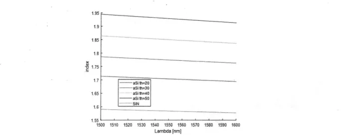
1.65 17, i tfr=20 aSi ft30 1.65 aSI th-40 -asi ui=5a 16 SIN 1500 1510 1520 1530 1540 1550 1560 1570 1580 1590 1600 Lambda [nm
Figure 3.3: Wavelength and thickness dependence of refractive index of a-Si layer.
I use the TE mode (where the magnetic field is pointing out of plane, i.e., E, = 0 and Hx = HY = 0). This mode is the fundamental mode of the waveguide. Because the electric field is in plane, this mode also maximizes the index contrast between SiN and a-Si, giving us a greater index contrast and thus a greater range of the refractive index. For the waveguide slabs, the effective indices of SiN and a-Si are shown in Figure 3.3 as a function of wavelength and a-Si thickness.
By changing d in the photonic crystal, we tune the dispersion w(k) and thus the effective index. For periodicity a = 400 nm, the hole diameter can range from dmai = 100 nm to
function of d and t. Here, I refer to "3D" as simulating the full 3D structure of the photonic crystal unit cell. For comparison, I also analyze the unit cell using 2D simulations where the hole region and a-Si regions use the 2D effective indices of SiN and a-Si slabs, respectively. The 2D effective indices are also shown in Figure 3.4. These are used to build 2D simulations which are more computationally feasible relative to full 3D simulations. The plot of neff for the 2D dispersion is extended out to d = 350 nm so that it contains the full range of neff of the 3D dispersion. C '3) 0 C a, C, Figure d. 1.95- 1.9- 1.85- 1.8- 1.75-1.7 1.65 1.6 - 3D, t=20 nm ' - - 2D, t=20 nm -3D, t=30 nm - - -2D, t=30 nm -3D, t=40 nm - - -2D, t=40 nm -3D, t=50 nm - - -2D, t=50 nm 100 150 200 250 300 350 Diameter of hole, d [nm]
3.4: Dependence of the refractive index of the photonic crystal as a function of t and
(h~i 1.0005 1.00005 0.99995 0.9995 CC 0.9999 0.999 -- t=20 nm 0.99985 0.9985 --t=30 t=40 nm nm 0.9998 -t=50 nm 0.998 0.99975-100 150 200 250 300 350 100 Diameter of hole [nm]
Figure 3.5: Anisotropy of the photonic crystal as measured indices at the K and M points in (a) 3D and (b) 2D.
-t=20 nm --- t=30 nm ---t=40 nm -- - t=50 nm 150 200 250 300 350 Diameter of hole [nm]
by the ratio of the effective
The triangular lattice was chosen because it has the highest degree of symmetry for 2D lattices and thus minimizes anisotropic behavior. The anisotropy of the photonic crystal
refractive index is illustrated in Figure 3.5(a) through a plot of nm/nK, where nM and nK
are the effective indices extracted along the F - M and F - K edges in the reciprocal lattice. The anisotropy. increases with t which is expected since the electromagnetic behavior of the photonic crystal deviates further from that the isotropic SiN slab as t increases. However, the anisotropy is less than 0.2% across all parameter ranges of interest, so we can ignore anisotropic effects in our modeling. The anisotropy of the photonic crystal modeled in 2D is less than 0.03%, so this is a valid substitute model of the 3D system assuming negligible anisotropy. (a) 1.26 (b) 1.012 t=20 nm 1 --- t=20 nm 1.24 m1.01 --- -3 -t=40nm -t=40 nm -- t=50 nm 1.2 1.006 C 1.18 1.004 -1.16 1.002 1.14 1 100 150 200 250 300 100 200 300 400
Diameter of hole [nm] Diameter of hole [nm]
Figure 3.6: Validity of the effective index approximation of the photonic crystal as measured by the ratio of phase to group index in (a) 3D and (b) 2D.
To further validate the assumption of an effective index, I compare the phase index of the photonic crystal to its group index ng = - where v9 = is the group velocity. In the
regime where the use of an effective index is valid, the dispersion should be linear such that
VP = vg and thus nr = ng. The ratio np/ng is plotted in Figure 3.6 for both the 3D model
and the equivalent 2D model. For the 3D model, the ratio increases with t and is on the order of - 20% which is not negligible. Because we are interested in the lensing behavior,
i.e., how the phase front is transformed by the lens, I use the phase index as opposed to the group index for designing the lens. The 2D model shows a relatively small ratio of - 1%, so
2D simulations will fail to show the effects of this discrepancy. However, because the lens is such a small structure relative to the entire system (as opposed to a waveguide), the effects
of the group index can be ignored.
3.3
Photonic Crystal Lens
(a) (b) 300 -Desired n neff achieved 250 1. ~ 200 a) 0 -6 150 1.05 100 70 E 50 1 0 0 0.2 0.4 0.6 0.8 1 0 0.2 0.4 0.6 0.8 1
Radius r (normalized) Radius r (normalized)
Figure 3.7: (a) Luneburg lens index profile for s = 2.8 (blue) and the effective index achieved
by the photonic crystal (orange). (b) Photonic crystal d as a function of lens radius to achieve the Luneburg lens index profile.
To build the lens using the photonic crystal, the hole size is slowly varied across the lens to realize the GRIN structure. In particular, a triangular lattice with periodicity a is superimposed on the lens, and at each unit cell in the lattice, the required refractive index of the lens is calculated and the hole size d is determined to match that index. If d required is outside of the range 100 nm to 300 nm, then d is either (1) truncated to the ends of the range 100 nm to 300 nm, (2) set to d = 0 nm (solid a-Si slab with no holes), or (3) set to d = oc (SiN slab without an a-Si layer).
An example of a Luneburg lens index profile with s = 2.8 and the realized index profile by the photonic crystal are shown in Figure 3.7(a) and the corresponding d is shown in Figure 3.7(b). We can see for r < 0.31R, the desired index profile is too high to achieve for the photonic crystal and so we set d = 0 nm (a-Si slab with no hole). In the range 0.31R <
r < 0.41R, the index is approximated with d = 100 nm. In the range 0.90R < r < 0.97R, the index is approximated with photonic crystal of d = 300 nm. In the range r > 0.97R, the desired index is too low for the photonic crystal and so we set d = oc, which is just the SiN
slab. Because the surrounding medium is also the SiN slab, this is equivalent to truncating the radius of the lens. The resulting lens is shown in Figure 3.8(a). Figure 3.8(b) shows the case for s = 5. Note that the lens truncation is more apparent for s = 5 because a larger s
requires a lower desired index.
(a) (b)
Figure 3.8: Photonic crystal implementation of the Luneburg lens with R = 10 Jim. Black
represents the a-SI slab while white represents the SiN slab. (a) s = 2.8. The index profile is shown in Figure 3.7. Note the region in the center of the lens where d = 0 Jim and it is a solid a-Si slab. (b) s = 5. The dotted line represents the desired perimeter of the lens, but the desired the index is too low to achieve with the photonic crystal and so the lens region is truncated.
3.4
Other Photonic Crystals
Other photonic crystal structures were considered to implement the GRIN lens. A triangular lattice of posts would achieve a range of refractive indices lower than that of the lattice of holes. Combining both holes and posts would thus achieve a greater total range of refractive indices, giving us greater flexibility in design. However, from a fabrication perspective, it is easier to use just one type of photonic crystal because each type of shape (holes versus posts) needs to be calibrated separately. Thus, for simplicity, we opted to use only a lattice of holes. We will see in the next section that truncating the lower range of effective index does not significantly harm the performance of the lens.
lattice and thus minimizes anisotropy, non-regular lattices were also considered including concentric rings of holes or posts and randomized positions of holes or posts. However, while non-regular lattices can decrease anisotropy or reduce unwanted diffraction orders [65], they
are often much more complex to design.
(a) (b) .1 I. d 60 * d 2d/3 d d/3.-I.
Figure 3.9: (a) Cross and (b) 3-stepped cross shapes for a triangular lattice. The crosses are inscribed in a regular hexagon (inner dotted line) which is concentric with and oriented the same way as the hexagonal unit cell that it lies in (outer dotted line). The dimensions of the crosses are determined by a single parameter, d.
(a) C 0 0 (V 0 a, -C C ~~0) CI, 0 LI C .003 1.002 1.001 (b) th=20 - th=30 -th=40 a: 0 0 , 0 X _0 6. P 1.0005 0.9995 0.999 0.9985 7 th=20 -th=30 -- th=40 -th=50 100 150 200 250 300 Diameter of hole/cross [nm] 10098 100 150 200 250 300 Diameter of hole [nm]
Figure 3.10: (a) Ratio nross/nhole where neross and nhole are the refractive indices of the cross and circular hole-based photonic crystals, respectively. (b) Ratio ncross/nhole where ncross and nhole are the refractive indices of the 3-stepped cross and circular hole-based photonic crystals, respectively.
Another photonic crystal structure I considered is a triangular lattice of holes where the holes are not circular, such as crosses or 3-stepped crosses as shown in Figure 3.9. The
: I
_JDL
ID
ID
1r-r--
D-boundaries of these unit cells are aligned with the Cartesian coordinates which simplifies the process of physically writing the lithography mask because the laser or electron beam that etches the mask usually travels along the Cartesian coordinates. The size of these non-circular holes is defined by d and can range from dmin = 100 nm to dmax = a - 100 nm based on the minimum feature size and minimum gap size. The refractive indices of these alternate photonic crystals is very similar to that of the circular-hole photonic crystal for a given d as shown in Figure 3.10. (a) (b) 0..998 0.99998-0o 0 th=20 .~0.996-.0 0.994 -0 th=30 -th=20 th=40 -- th=30 0.992 -th=50 -th=40 0.994 - -- th=50 0.99 100 150 200 250 300 100 150 200 250 300
Diameter of hole [nm] Diameter of hole [nm]
Figure 3.11: Anisotropy of the photonic crystal as illustrated by the ratio nM/nK for (a) the cross photonic crystal and (b) the 3-stepped cross photonic crystal.
The anisotropy of these alternate photonic crystals are shown in Figure 3.11. Both structures are more anisotropic than the circular-hole photonic crystal, as suspected, because the new structures reduce the symmetry from 6-fold to 4-fold symmetry. However, the anisotropy is still small enough that it can be safely ignored.
For simplicity of analysis, I implement the lens using the circular-hole photonic crystal. However, as previously stated, the alternate photonic crystals can be simpler and faster to implement in fabrication.
Chapter 4
Methods for Lens Simulation
To characterize and optimize the lens performance, simulations of the lens are carried out us-ing the finite-difference time-domain (FDTD) method usus-ing MEEP, an open-source software package [66]. MEEP is a full-wave electromagnetic solver that simulates the electromag-netic fields exactly using Maxwell's equations. While ray-tracing is often used to simulate electromagnetic phenomena such as lens behavior, it is only valid in the limit where feature sizes are much larger than the wavelength of light. Photonic crystals by definition have sub-wavelength features and so we must treat it using Maxwell's equations to study the effects of the photonic crystal.
Because full-scale 3D simulations of the lens are prohibitively computationally expensive, 2D simulations are used to simulate the lens. The effective refractive indices of the a-Si and SiN slabs are used in place of the bulk indices for a-Si and SiN. The hole sizes are determined using the 2D effective indices plotted in Figure 3.4 while also being constrained to the index ranges of the 3D structure.
The 2D MEEP simulations implement open boundaries using a perfectly matched layer (PML) with a thickness of 1 pm. The boundaries of the simulation 10 im away from the edges of the lens. The resolution of the simulation is 30 mesh cells per pm. Increasing these values do not make any appreciable difference to the simulation results. The waveguide that
feeds into the waveguide slab is 5 pm long and 1 jim wide. To accurately represent the source, I take advantage of MPB's integration with MEEP to calculate the fundamental mode of the waveguide, and use a current source that excites this mode. The point at which the waveguide feeds into the waveguide slab is placed at the focal point of the lens.
(a) (b)
Figure 4.1: (a) Permittivity profile of the 2D simulation in MEEP. Black is a-Si, grey is SiN, and white is SiO2. (b) Resulting magnetic field, Hz of the MEEP simulation.
The permittivity profile of the simulation along with the resulting magnetic field H, are shown in Figure 4.1 for a lens with radius R = 5 rim. This small size is chosen to display the photonic crystal structure in the lens. We can see from the H, profile that the waveguide mode spreads after it enters the waveguide slab, passes through the lens, and is collimated on the other side of the lens. There is some energy that does not impinge on the lens and thus does not get collimated. Additionally, there appears to be diffraction of the electromagnetic field in and around the lens due to the small size of the lens, but these effects become insignificant as the lens size increases.
The far field is calculated in MEEP by using a Fourier transform to extend the fields out 1 m from the edge of the simulation along all 4 boundaries of the simulation. This is far enough such that any Gaussian beam with a waist size equal to the lens radius we are simulating reaches the far field, allowing us to measure the far field beam divergence accurately. A polar plot of the farfield of a lens with radius R = 30 Jim is shown in Figure 4.2(a), where the angle 0 = 0' is aligned with the x-axis. The farfield is normalized to the
maximum power. collimation of the
(a)
We can see that most of the energy is in the main lobe, demonstrating
lens. 135' 45* 0 180* 0. 225' 31.5' 270' (b) 0 -5 -20 -25 -30 Frctonpoerwihi FHM=0.47 Sidelobe level = -11.9 dB -20 -15
Figure 4.2: Farfield plots for a lens with radius R = 30 pm. the SiN slab. (b) Farfield corrected for air and zoomed into
0 -5 0 5
Agle [deg]
(a) Polar plot the main lobe.
of the farfield in
The background and boundaries of the simulation are in the SiN slab. However, we want to know how the beam behaves when it exits the chip into air. Thus, we correct for this using Snell's Law by multiplying the angle of the farfield plot by the effective refractive index of SiN. A farfield plot corrected for air and zoomed into the main lobe is shown in Figure 4.2(b). To measure the degree of collimation of the outgoing beam from the lens, we use the -3dB farfield beamwidth, also known as the full-width half-max (FWHM), as our primary figure of merit. The FWHM is proportional to the beam divergence and gives us a measure of how well collimated. the beam is and thus the resolution of beam steering that can be achieved. The remainder of the farfield plots shown in this thesis are corrected for air.
(a)
Chapter 5
Results
5.1
Lens Performance
There are three assumptions that we made when designing the lens: (1) the size of the lens is sufficiently larger than the wavelength of light such that we can approximate the light as rays (which is how the semi-analytical formulation of the Luneburg lens was derived), (2) the rays are emanating from a point source, and (3) the gradient-index lens is sufficiently realized by the photonic crystal. For reference, we simulate an "idealized lens" with the exact desired index of refraction at each point in the lens without discretization from a metamaterial or photonic crystal. The idealized lens achieves a true gradient index and fulfills our third assumption so that we can examine the first two assumptions in isolation.
To examine the first assumption, I run the lens setup "in reverse" using the idealized lens, in which I send a plane wave from the +x direction onto the idealized lens and analyze how the lens focuses the energy. This setup is shown in Figure 5.1 where we can see from the field profile and the energy profile that the wave is focused into a tight spot. The time-averaged energy density is calculated by pOiHj2/2, where H is the complex magnetic field.
The focal length of the lens is measured by calculating the location of the maximum in the magnetic field energy density. The error in the measured focal length relative to the
(a) (b)
Figure 5.1: Simulation of the lens (gray) with a plane wave sent in from the right so that we can see focusing. (a) H, profile (red and blue). (b) Time-averaged magnetic field energy density, toIH12/2 (orange).
(a) -0.25- 0.500.75 --1.00 ---1.25 -0 .5 -1.50-u -1.75- -2.00-30 40 50 60 70 R 19m] 80 90 100 (b) - 2.4 E a 02.2 a 1.8 0 5 1.6 S1.4 4. 1.2 r 1.0
Figure 5.2: Results of sending in a plane wave into the lens and measuring the focused field. (a) Error in the focal length measured by the location of the maximum field. (b) Resolution criterion of the focused field as measured by the distance from the maximum field to the first minimum, 6, and the analytical solution for the Rayleigh diffraction limit. The points for R = 50 pm and R = 100 jim are overlayed on each other and thus cannot be seen separately.
S s =23 s =3 . s 4 Analytical " R = 25 pm - R = 50 pm - R = 100 pm 2.00 2.25 2.50 2 75 3.00 3.25 3.50 3.75 4.00
designed focal length is plotted in Figure 5.2(a) for various R and s. Surprisingly, despite our expectations of smaller diffraction effects for larger lenses, the error appears to increase for larger lenses, which is an area for further investigation. However, while the absolute error increases for larger lenses, the error when normalized to the lens radius decreases.
Additionally, at the measured focal length, I take a cross-section of the energy density transverse to the beam propagation direction and measure the Rayleigh resolution criterion, which is the -distance from the maximum to the first minimum. The analytical solution for the Rayleigh diffraction limit is:
0.61A0
n usinO0
where A = 1.55 pim is the wavelength in free space, n 1.584 is the effective index inside the SiN slab, and 0 = arctan
(1)
is the half-angle of the focused beam. The measured and analytical Rayleigh resolution limits are plotted in Figure 5.2(b). Interestingly, the measured resolution limit is better than the analytical resolution limit. This may be due to the analytical limit assuming a uniformly illuminated aperture which produces a sinc function at the focal point. Implicitly, this also assumes a flat lens. However, the Luneburg lens is not flat and focuses the fields inside the lens, thus resulting in a non-uniform energy profile at the exit aperture of the lens. We can conclude that approximating the light as rays is a valid approach to designing the lens index profile and that the idealized lens is a diffraction-limited system.To examine the second assumption, I use a dipole source at the point of the idealized len's designed focal lens and analyze how well the beam is collimated. Figure 5.3 shows the permittivity profile of a simulation where a dipole source is placed at the focal point of the lens and the resulting H, field. The dipole source emits isotropically and the field that impinges on the lens is collimated. As seen in Figure 5.4, the farfield FWHM of the collimated waveguide source is much larger than that of the collimated dipole source, demonstrating that the waveguide does not approximate a point source very well. This is expected as the
Figure 5.3: H, (red and blue) overlayed on the permittivity profile (greyscale) of a simulation of a dipole source and an ideal lens with s = 2 and R = 25 pm.
2.00 1.75-1.50 1.25- U-.U 1.00 0.75 0.50 * dipole s= 2 a dipole, s = 3 * dipole, s = 4 Analytical * WG, s = 2 * WG, s = 3 e WG, s =4 S.. +++ .. 30 40 50 60 70 80 90 100 R [pmj
Figure 5.4: Far field FWHM of the collimated beam using an ideal lens and both a dipole source and waveguide (WG) source. The dotted line is the analytical FWHM assuming a uniformly illuminated aperture, which results in a sinc function pattern in the farfield.
waveguide mode has a non-zero width, and this mode propagates in a non-trivial way once it exits the waveguide.
Interestingly, the dipole farfield FWHM is approximately constant as a function of s for a fixed value of R, whereas the waveguide farfield FWHM decreases as s increases for a fixed value of R. This is because for a small s, the waveguide beam does not fully illuminate the lens, decreasing the effective aperture and increasing the farfield FWHM. For larger s,
the waveguide beam fully illuminates the lens so the lens sees a more uniform source. The tradeoff is that some of the energy from the waveguide may miss the lens, thus increasing losses in the system.
(a) (b) 100 _ 5 0--50 --100 -0 100 200 300 400 560
Figure 5.5: Behavior of a waveguide mode traveling from a waveguide into a waveguide slab. (a) H, (b) Streamlines of the time-averaged Poynting vector, S. Only vectors above an aribtrary threshold are plotted to better visualize the beam in the lab. The point at which the waveguide meets the slab waveguide is at x = 0.
To characterize the output from the waveguide, I simulate the waveguide mode as it travels from the waveguide into the slab waveguide without a lens. The time-averaged Poynting vector is calculated as S = !R (E x H*) where E and H are the complex electric
43
and magnetic fields,. respectively. The H, field and a streamline plot of S are shown in Figure 5.5 which shows the beam spreading as it exits the waveguide. Additionally, the streamline plot contains straight vectors across the entire beam, which suggests that we can approximate the beam using ray optics and find the focal point of these rays.
0.6- 0.4- 0.2-0.0 -0.2--0.4- - x=400 pm x=200 pm - x=100 pm -0.6--100 -50 0 50 100 y [pml
Figure 5.6: The predicted focal point at each yi along several slices in xi.
At each point in the slab waveguide (xi, yi) (in units of lim) where (xi = 0, yi = 0) is at the point where the waveguide meets the waveguide slab, we calculate where a ray parallel to S would intersect the line y = 0 which represents the focal point xf:
_YiSX Xf
Xi-where Sx and Sy are the x and y components of S. This quantity is plotted as a function of yi for various cuts along the x-axis in Figure 5.6. We can see that most of the vectors point away from x = 0 as expected. There is a dip at y = 0 showing that it does not represent a perfect point source. However, the shift is small so I do not adjust the waveguide position to account for this.
Finally, to examine the final assumption, I simulate the lens constructed with the photonic crystal. Figure 5.7 shows the field results for lenses built using various a. For now, we ignore the fabrication constraints on minimum feature size and gap size so that we are not
![Figure 1.1: Architecture of lens-based chip-scale LIDAR system. Figure from [30] @2017](https://thumb-eu.123doks.com/thumbv2/123doknet/14685153.560060/16.917.116.689.363.583/figure-architecture-lens-based-chip-scale-lidar-figure.webp)