HAL Id: hal-00001649
https://hal.archives-ouvertes.fr/hal-00001649
Submitted on 30 May 2004
HAL is a multi-disciplinary open access
archive for the deposit and dissemination of
sci-entific research documents, whether they are
pub-lished or not. The documents may come from
teaching and research institutions in France or
abroad, or from public or private research centers.
L’archive ouverte pluridisciplinaire HAL, est
destinée au dépôt et à la diffusion de documents
scientifiques de niveau recherche, publiés ou non,
émanant des établissements d’enseignement et de
recherche français ou étrangers, des laboratoires
publics ou privés.
in S/F/S junctions
Hermann Sellier, Claire Baraduc, Francois Lefloch, Roberto Calemczuk
To cite this version:
Hermann Sellier, Claire Baraduc, Francois Lefloch, Roberto Calemczuk.
Temperature induced
crossover between 0 and pi states in S/F/S junctions. Physical Review B: Condensed Matter and
Materials Physics (1998-2015), American Physical Society, 2003, 68, pp.054531. �hal-00001649�
Temperature-induced crossover between 0 and
states in S
ÕFÕS junctions
Hermann Sellier,*Claire Baraduc, Franc¸ois Lefloch, and Roberto Calemczuk
De´partement de Recherche Fondamentale sur la Matie`re Condense´e, CEA-Grenoble, 17 rue des Martyrs, 38054 Grenoble, France 共Received 6 May 2003; published 26 August 2003兲
Ferromagnetic Josephson junctions can show at equilibrium a phase difference between the supercon-ducting electrodes. We explain this state in an original way by a modified spectrum of Andreev bound states shifted by the exchange energy. A simplified expression for the spectral supercurrent density is calculated and the nonmonotonic temperature dependence of the critical current is discussed. This model accounts for the cancellation of the critical current with temperature observed in a small range of barrier thickness in our Nb/Cu52Ni48/Nb junctions. This cancellation corresponds to an inversion of the supercurrent and to a
ground-state crossover from a 0 ground-state to a state. This transition is caused both by the thermal distribution of quasiparticles and by the temperature dependence of the exchange energy. The experimental curves are well reproduced by our theoretical expression except for the very small amplitude of the supercurrent attributed to a large spin-flip scattering.
DOI: 10.1103/PhysRevB.68.054531 PACS number共s兲: 74.50.⫹r, 74.45.⫹c
I. INTRODUCTION
A Josephson junction at equilibrium has usually a phase difference gs⫽0 between the two superconductors, this property being related to the positive coefficient of the current-phase relation. A mechanism leading to a negative coefficient and a ground state with gs⫽ was first pro-posed in S/I/S junctions with magnetic impurities in the barrier,1 but any experimental evidence of this effect has never been obtained. Then S/F/S junctions were also pre-dicted to produce states for an appropriate ratio between the thickness dependent Thouless energy and the exchange energy of the ferromagnetic layer.2,3
The experimental study of S/F/S multilayers started with the use of high Curie temperature ferromagnets4and a sig-nature of the state was searched for in the ferromagnetic thickness dependence of the critical temperature. Nonmono-tonic behaviors of Tc were observed and attributed either to the state5 or to the onset of ferromagnetism.6 These ex-periments are indeed difficult to interpret because the large values of the exchange energy require very thin layers for which ferromagnetic properties are strongly thickness depen-dent. The conclusions of these studies regarding the exis-tence of the state remain controversial.
Recently, perpendicular transport measurements through the ferromagnetic barrier have been carried out on S/F/S Jo-sephson junctions with low Curie temperature ferromagnets. Ryazanov et al. observed a nonmonotonic temperature de-pendence of the critical current in Nb/CuNi/Nb junctions in-terpreted as a crossover between a 0 state and a state.7 They also placed five of these junctions in a double loop interferometer and observed a shift of half a flux quantum in the interference pattern.8 These results provide the first un-ambiguous proof of the existence of the state. More
re-cently similar results have been obtained in
Nb/Al2O3/PdNi/Nb junctions using the ferromagnetic
thick-ness dependence instead of the crossover in temperature which has not been observed.9,10
This paper presents both a theoretical analysis and an ex-perimental study of the transition between the 0 state and the
state in S/F/S junctions. In Sec. II we give an alternative explanation of thestate based on the Andreev bound-states spectrum instead of the superconducting correlation function considered in the previous works. The origin of the supercur-rent in S/N/S junctions derives indeed from the existence of these bound states in the normal metal.11The ‘‘sign’’ of the supercurrent can be directly deduced from the dependence of the Andreev spectrum with the phase difference. This ap-proach therefore provides an intuitive understanding of the ‘‘negative sign’’ of the critical current in S/F/S junctions re-sponsible for thestate. For clarity we will first consider the ballistic and one-dimensional case because the Andreev spectrum is easier to describe.
However, the experimental devices are in the diffusive regime and the distribution of Andreev bound states becomes more complicated. The significant quantity is the spectral supercurrent density which is closely related to the Andreev spectrum of the ballistic case. This function gives the super-current carried by the Andreev bound states at a given energy and was originally introduced to analyze nonequilibrium situations.12In Sec. III we calculate this spectral supercurrent density for S/F/S junctions using the linearized Usadel equa-tions and explain the ‘‘negative’’ critical current by an un-usual spectral behavior instead of a spatial oscillation of the superconducting correlation function.
We also consider the spectral approach instead of the Mat-subara formalism in order to clarify the temperature depen-dence of the supercurrent which is very unusual in S/F/S junctions. It should be noticed that the early theoretical works neglected the influence of temperature on the pair den-sity in the ferromagnetic region because the experimental studies focused only on large Curie temperature ferromag-nets. The investigation of low exchange energies is recent and the nontrivial influence of the temperature which can reverse the sign of the supercurrent requires a deeper analy-sis. This behavior has no obvious physical interpretation in the Matsubara formalism whereas the spectral approach pro-vides a simple explanation.13
In Sec. IV we present our experimental study of Nb/Cu52Ni48/Nb junctions with barrier thicknesses close to
the value inducing a crossover between the 0 state and the state. The critical current of these junctions has a nonmono-tonic temperature dependence with a complete cancellation at a temperature which depends on the thickness. This can-cellation actually corresponds to the sign change of the current-phase relation coefficient discussed in the theoretical part and whose consequence is a switch from the 0 state to thestate. This very unusual temperature dependence is the same as the one reported by Ryazanov et al.7However, they used a different copper-nickel alloy with a ferromagnetic be-havior, whereas our alloy is nearly superparamagnetic. Mea-surements of the critical current as a function of the magnetic field show typical Fraunhofer patterns centered around zero field at all temperatures. This confirms that the vanishing supercurrent is an intrinsic property of our S/F/S junctions and is not due to magnetic induction.
This interpretation as a 0 tocrossover is also supported by a comparison in Sec. V between the experimental data for different barrier thicknesses and the theoretical expression of the critical current calculated in Sec. III. We include the con-tribution of the temperature-dependent exchange energy be-cause the measured magnetization does not saturate at low temperature. The extremely small amplitude of the supercur-rent cannot be accounted for by the theoretical expression in its simplest formulation. It can however be reproduced if we include a strong spin-flip scattering which may be present in our superparamagnetic copper-nickel alloy.
II. EXPLANATION OF THE STATE USING THE ANDREEV BOUND STATES
A. SÕN and SÕF proximity effect
The wave function of the superconducting condensate at zero temperature is a coherent superposition of partially oc-cupied states in the energy range of the gap ⌬ around the Fermi level as can be seen from the BCS expression.14,15 Some of these states have therefore a wave vector above the Fermi level and can be injected in the normal metal at the S/N interface 共see Fig. 1兲. However, electrons can only be removed by pairs in a superconductor, so that a second elec-tron has to leave the condensate and it fills a hole state below the Fermi level in N. From the superconductor point of view, two electrons have been transferred from S to N, and from the normal-metal point of view, a hole in N has been re-flected into an electron in N. This mechanism of charge transfer at the S/N interface is called an Andreev reflection.16 The symmetric case is also involved in which an electron above the Fermi level in N cross the S/N interface and a hole is left共Andreev reflected兲 below the Fermi level in N.
We discuss now the phase coherence of an electron and a hole correlated by an Andreev reflection. At the Fermi level, the two particles have the same wave vector ke⫽kh and fol-low exactly the same path with opposite group velocities. The relative phase of their wave functions is constant along this path and the coherence length of the pair is very long
共limited by the phase breaking length L). If the electron is
at finite energy 0⬍⑀⬍⌬ with a wave vector ke(⑀)⫽kF
⫹␦k where␦k⫽⑀/ប vF, the hole has the same energy⑀but below the Fermi level and has therefore a smaller wave
vec-tor kh(⑀)⫽kF⫺␦k. This difference produces a relative phase shift in the Andreev pair equal to 2␦k x. This shift reduces the coherence length in the diffusive regime because the elastic diffusions scatter the two particles differently when their phase difference becomes larger than unity共or equiva-lently when the particles become separated by more than a Fermi wavelength兲.
In a ferromagnetic metal, the two spin subbands are split by the exchange energy ⫾Eex and they have Fermi wave vectors equal to kF⫾q where q⫽Eex/បvF. Because the electron and the hole of an Andreev pair are in opposite spin subbands, their wave vectors are now equal to
再
ke↓共⑀兲⫽kF⫺q⫹␦k, kh↑共⑀兲⫽kF⫹q⫺␦k, and再
ke↑共⑀兲⫽kF⫹q⫹␦k, kh↓共⑀兲⫽kF⫺q⫺␦k, 共1兲for the two types of pairs.17At the Fermi level, they have a phase shift 2qx which is responsible for a short coherence lengthF⫽
冑
បD/Eexin the diffusive regime. However at the particular value ⑀⫽Eex, the excitation energy for pairs with spin-down electrons is exactly compensated by the exchange energy because ␦k⫽q. The wave vectors ke↓(Eex) for the electron and kh↑(Eex) for the hole are both equal to kFand the internal phase shift disappears. A long coherence length can therefore be recovered in case of a small exchange energy Eex⬍⌬.FIG. 1. Electron and hole wave functions of an Andreev pair which forms a bound state in an S/N/S junction. The gray areas represent the distribution of occupied states at zero temperature. An electron is injected from the superconductor into the normal metal above the Fermi level and a hole is captured below at the same time. A bound state is formed when the wave functions satisfy the boundary conditions imposed by the superconducting phases 1
B. Andreev bound states in SÕNÕS junctions
In a ballistic normal metal placed between two supercon-ducting electrodes, the Andreev reflections at the two inter-faces create discrete bound states.18 The spectrum of these levels is sensitive to the superconducting phase difference between the electrodes ⫽2⫺1 as described in the following.11,19–21 The wave function of an Andreev state at energy 0⬍⑀⬍⌬ is evanescent in S and propagates in N 共see Fig. 1兲. At the S1/N (N/S2) interface, the relative phase
⫽e⫺hbetween the electron and hole components is equal to the macroscopic phase 1 (2) of the superconductor, plus an additional term⫺(⫹)arccos⑀/⌬ due to the evanes-cent part of the wave in S. In a ballistic and one-dimensional S/N/S junction, going from one interface to the other, the relative phase of the pair changes by⌬⫽2␦k d, where d is the length of normal metal and ␦k⫽⑀/ប vF. A bound state appears at energy⑀nif this phase shift⌬matches the phase difference at the two interfaces, modulo 2. For a pair with a wave vector in the opposite direction, the phases 1 and
2have to be exchanged. The discrete Andreev bound states
for positive and negative wave vectors are given by
⌬⫽2 ⑀n
ប vF
d⫽⫾⫹2 arccos⑀n
⌬ ⫹2n. 共2兲
There is no state at⑀⫽0 for⫽0 because there is no phase shift during the transport across the normal metal whereas the phase difference imposed by the two interfaces should be equal to. At⑀⫽⌬ no phase shift is required and a bound state is possible even for a very short junction where ⌬
⫽0. Two successive levels are separated by ETh 共for ⑀
Ⰶ⌬) where ETh⫽បvF/d is the Thouless energy. At zero temperature, electrons can be injected above the Fermi level from the superconducting electrodes thanks to the distribu-tion of occupied states in the condensate. The corresponding holes of the pairs are below the Fermi level and carry cur-rents in the same direction because they have opposite charge and group velocity. An Andreev state with k⬎0 car-ries a charge ⫺2e in the direction of its wave vector and therefore a negative current. For this reason we call (⫺) the states k⬎0 and (⫹) the states k⬍0. For⫽0, the (⫹) and (⫺) states are degenerate and there is no resulting current. For ⬎0, the energy of the (⫹) states decreases, whereas the energy of the (⫺) states increases, and the spectrum alternates levels with opposite currents as shown in Fig. 2共a兲. Since the lowest levels are the most occupied, the normal metal carries a finite and positive current which is called ‘‘supercurrent’’ because no voltage is required. An important point to remember for the following is that the direction of the total current is given by the first level. The current is maximum for ⫽⫺ when this first level reaches ⑀⫽0⫹. For ⫽⫹ this (⫹) level disappears and a (⫺) level ap-pears at⑀⫽0⫹. As a result, the current-phase relation shown in Fig. 3共a兲 is a 2-periodic function with a sawtooth shape at zero temperature in this ballistic regime.
C. Andreev bound states in SÕFÕS junctions
In ferromagnetic junctions, the phase shift of the Andreev pairs contains the additional term⫾2qd due to the exchange energy and Eq. 共2兲 has to be changed into
⌬⫽2⑀⫾Eប vex
F
d⫽⫾⫹2 arccos⑀
⌬ ⫹2n. 共3兲
For the (↑↓) pairs with a spin-up electron and a spin-down hole, the additional phase shift is positive and thus the bound
FIG. 2. Discrete spectrum of Andreev bound states in a long one-dimensional ballistic共a兲 S/N/S junction and 共b兲 S/F/S junction with Eex⫽(/2) ETh. Each degenerate state is split by the phase
difference ⫽/2 into states carrying currents in opposite direc-tions. The first state above the Fermi level has the largest contribu-tion to the total supercurrent which is positive for the S/N/S junc-tion and negative for the S/F/S juncjunc-tion.
FIG. 3. 共a兲 Current-phase relation at zero temperature and the corresponding energy-phase relation for a long one-dimensional ballistic S/N/S junction and for an S/F/S junctions with Eex
⫽(/2) ETh. The ground states are, respectively, the 0 state with
gs⫽0 and the state with gs⫽. 共b兲 These two states are
degenerate at the crossover for Eex⫽(/4) ETh, but the critical
states move to lower energies. Similarly, for the (↓↑) pairs, they move to higher energies. Each level is therefore split into its two spin components.
In the following, we consider the particular value Eex
⫽(/2)ETh and analyze the modification of the Andreev spectrum as shown in Fig. 2共b兲. For⫽0 the first level (↑↓) is shifted from (/2)ETh to 0 because the additional phase shift 2qd gives exactly the appropriate value ⌬⫽ to match the boundary conditions with the superconductors. When the phase difference increases, the (⫹) state disap-pears immediately below the Fermi level and the (⫺) state rises above carrying a current in the negative direction. This shifted spectrum with an Andreev bound state at zero energy is therefore responsible for a negative supercurrent at posi-tive phase difference.
The current-phase relation and also the energy-phase re-lation given by dE/d⫽(ប/2e)IS are translated by com-pared to the normal case as shown in Fig. 3共a兲. The mini-mum of the energy corresponding to the ground state is obtained forgs⫽共instead ofgs⫽0 for normal case兲 and this S/F/S junction is therefore called a junction. This de-scription using the Andreev bound states shifted by the ex-change energy provides from our point of view a deeper understanding of the origin of the state than the previous works on this subject.
The Andreev spectrum in this ground state is obtained by setting ⫽ in Eq.共3兲 and is therefore identical to the spectrum of an S/N/S junction with Eex⫽0 andgs⫽0. The additional phase shift 2qd⫽ is compensated by the phase differencegs⫽. In particular the first bound state is not at
⑀⫽0. The situation would be different in an S/F bilayer
be-cause this system corresponds to an S/F/S junction always at
⫽0 共and two times thicker兲. As a result, the density of state
which is always minimum at ⑀⫽0 in S/N systems can be maximum at ⑀⫽0 in the S/F case because of the shifted bound states. This ‘‘reversed’’ density of states has been ob-served experimentally in diffusive Nb/PdNi bilayers.22
Finally we briefly discuss the situation of an exchange energy equal to (/4)ETh. The level spacing of the Andreev bound states for ⫽0 is two times smaller and the current-phase relation has a period of as shown in Fig. 3共b兲. The 0 state and thestate are degenerate but the critical current is nonzero at the crossover in this ballistic regime.
III. TEMPERATURE-INDUCED CROSSOVER IN DIFFUSIVE REGIME
A. Spectral supercurrent in SÕNÕS junctions
In the diffusive regime the Andreev bound states have a continuous distribution and induce a spectral supercurrent density NJ(⑀) in the normal metal.12,23In the following, we derive a simplified expression for NJ(⑀), by first calculating the supercurrent in the Matsubara formalism and then by transforming the expression in real time formalism.
The nonlinear Usadel equations24for the Green functions G(n,x) and F(n,x) can be solved by numerical calcula-tion in the general case. However for a better analysis of the result, an analytical expression for the supercurrent is more
convenient, but requires some approximations. We suppose a small amplitude of the induced correlations in the normal metal and linearize the equations with G⬇1 and FⰆ1. In principle, this approximation is only valid for temperatures larger than the gap, close to the superconducting transition. However, it can also be used at all temperatures for the cal-culation of the supercurrent if the exact numerical values are not needed. We also assume a perfect transparency of the S/N interfaces at x⫽⫾d/2 and do not solve self-consistently the order parameter in the superconductors. We calculate the supercurrent as done in Ref. 25 using the following equa-tions wheren⫽(2n⫹1)kBT: IS共T兲⫽2kBT e RN
兺
n⬎0 Im关d F*“F兴 共4兲 ⫺បD2 ⵜ2F⫹ nF⫽0, 共5兲 F共⫾d/2兲⫽ ⌬冑
⌬2⫹ n 2e⫾i /2. 共6兲In real time formalism, the supercurrent is expressed as an integral over the energies⑀ instead of a sum over the Mat-subara frequencies n. The spectral supercurrent density NJ(⑀) corresponds to the term in the sum in Eq. 共4兲 where
n is replaced by ⫺i(⑀⫹i␥). The parameter ␥⫽0⫹ sup-presses the singularities and comes from the retarded Green functions involved in the spectral densities. In this formalism the supercurrent is now given by the following expressions (␥ is removed when not necessary兲:
IS共T兲⫽ 1 e RN
冕
0 ⫹⬁ NJ共⑀兲 h共⑀兲d⑀, 共7兲 NJ共⑀兲⫽Im冋
⌬2 ⌬2⫺共⑀⫹i␥兲2冑
⫺2i⑀/ETh sinh冑
⫺2i⑀/ETh册
sin, 共8兲 h共⑀兲⫽1⫺2 fT共⑀兲⫽tanh共⑀/2kBT兲. 共9兲 The spectral supercurrent density is plotted in Fig. 4共a兲 in the long junction case EThⰆ⌬ with a Thouless energy in the diffusive regime ETh⫽បD/d2. Only positive energies have a physical meaning but we also plot the function for negative energies to simplify the transition to the S/F/S case. The oscillations correspond to the previously discussed (⫹) and (⫺) discrete bound states split by the phase difference ⫽/2 and carrying the current in opposite directions. The exponential decay comes from the diffusive regime where the coherence of the Andreev states at energy ⑀ is broken beyond a characteristic length l⑀⫽
冑
បD/⑀. The linearization of the equations is responsible for the absence of a minigap around ETh and for a current-phase relation proportional to sin. The critical current is obtained for⫽/2.At zero temperature, all the states are available and the total supercurrent is the integral of NJ(⑀). At finite tempera-ture, quasiparticle states are occupied by thermal excitations
according to the Fermi distribution fT(⑀). The available en-ergies for the coherent Andreev bound states are above these excitations and are given by the function h(⑀). Some An-dreev levels are therefore suppressed and the supercurrent decreases with increasing temperature in a monotonic way as shown in Fig. 5.
The oscillations of the spectral supercurrent density have been taken advantage of to change the sign of the Josephson current.26 A transverse voltage is applied to the mesoscopic normal metal of an S/N/S junction at low temperature and an out-of-equilibrium distribution function with two sharp steps is produced. For a voltage equal to the first node of NJ(⑀), the large positive contribution is suppressed, whereas the small negative one at higher energy is still fully active and the sign of the total supercurrent is reversed. The negative supercurrent of ferromagnetic junctions also comes from these oscillations of the spectral supercurrent density, but in a
different way: the shift of h(⑀) induced by the voltage is replaced by a shift of NJ(⑀) induced by the exchange energy.
B. Spectral supercurrent in SÕFÕS junctions
The exchange energy Eexincreases or decreases the phase shift of the Andreev pairs and affects not only the position of the bound states but also their coherence in this diffusive regime. This coherence is maximum when the excitation en-ergy of the Andreev pair and the exchange enen-ergy compen-sate each other. The spectral supercurrent density is shifted to higher energy by ⫹Eex for the (↓↑) pairs and to lower en-ergy by⫺Eex for the (↑↓) pairs. The total supercurrent den-sity is the sum of the two spin contributions:
NJ共⑀兲⫽Im
冋
⌬2
⌬2⫺共⑀⫹i␥兲2
冉
冑
⫺2i共⑀⫹Eex兲/ETh sinh冑
⫺2i共⑀⫹Eex兲/ETh⫹
冑
⫺2i共⑀⫺Eex兲/ETh sinh冑
⫺2i共⑀⫺Eex兲/ETh冊
册
sin. 共10兲
In the long junction case EThⰆ⌬, the first term contain-ing the gap is close to unity, so that NJ(⑀) in the S/F/S case is simply the sum of two shifted functions of the S/N/S case. The corresponding function is shown in Fig. 4共b兲. The large negative peak which was below the Fermi level in the S/N/S case is now above and gives a negative contribution. This mechanism is the same as in the ballistic case where the first bound state above the Fermi level is a (⫺) state for⬎0. Since the area of the negative part of the function is slightly larger than that of the positive one, the sign of the total supercurrent IS is negative at zero temperature and the ground state of the junction is a state.
At finite temperature, the spectral supercurrent density is multiplied by the distribution function h(⑀). The
contribu-FIG. 4. Spectral supercurrent density for ⫽/2 共solid line兲 and distribution function for kBT⫽5 ETh 共dashed line兲 in long 共a兲
S/N/S junction and 共b兲 S/F/S junction with Eex⫽13EThⰆ⌬. The
vertical bars illustrate the relation with the discrete Andreev bound states of the ballistic regime: the (⫹) and (⫺) states carrying cur-rents in opposite directions are split by the phase difference. In the S/F/S case the two spin components of the spectral density are shifted by⫾Eex. Only the positive energies have a physical
mean-ing and enter in Eq.共7兲.
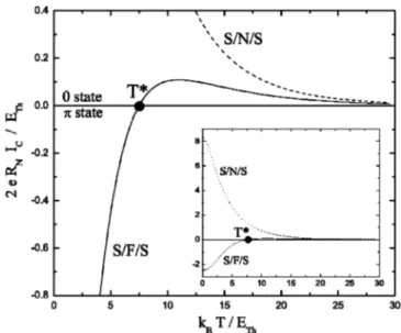
FIG. 5. Crossover between 0 and states at a temperature T*
resulting from a nonmonotonic dependence of the critical current in a long S/F/S junction with Eex⫽13 EThⰆ⌬ 共solid line兲, compared
to the monotonic behavior of S/N/S junctions 共dashed line兲. The inset shows the same curves on a larger scale.
tion of the negative part just above the Fermi level is reduced because the Andreev levels at low energy are partially sup-pressed by the thermal excitations. The positive part be-comes dominant and reverses the sign of the total supercur-rent. When the temperature is increased, the critical current varies continuously from a negative value to a positive one and changes sign at a crossover temperature T*as shown in Fig. 5. Such a junction is in the state at low temperature and in the 0 state above T*.
It is important to notice that this behavior is possible only in the S/F/S case because the negative and positive contribu-tions of the spectral supercurrent density have nearly the same amplitude. This property is due to the decoherence of the diffusive regime which is canceled at⑀⫽Eex共zero inter-nal phase shift兲. In the S/N/S case, because the exponential decay is centered at ⑀⫽0, the positive part is much larger than the negative one and the supercurrent is always positive as a function of temperature. An out-of-equilibrium situation induced by a voltage is required to obtain an S/N/S junc-tion as already menjunc-tioned.
The additional phase shift of the Andreev pairs due to the exchange energy corresponds to a spatial oscillation of the anomalous Green function F(n,x) calculated in Matsubara formalism. This function describes the superconducting cor-relations
具
↑(x)↓(x)典
in the normal metal, but the intrinsic oscillations due to the excitation energy⑀are suppressed by an integration at thermal equilibrium. On the other hand, the additional relative momentum 2q is identical for all the An-dreev pairs and survives to this integration. It induces an oscillatory behavior with a period related to F⫽冑
បD/Eex as explained in Ref. 17. This spatial oscillation can connect the two superconducting order parameters with opposite signs and produce a state when d⬃F 共equivalent to ETh⬃Eex). However, this intuitive explanation
3,7,27does not
ex-plain the electronic process involved in the Josephson cou-pling. A more physical understanding can be obtained with the Andreev bound states as presented in this paper. More-over, the spectral approach is necessary to understand the temperature induced crossover between the 0 state and the state.
C. Short junction case and large exchange energy
The above analysis was done in the long junction case with Eex⬇EThⰆ⌬0. We now discuss the case of an
interme-diate exchange energy Eex⬃⌬0corresponding to our
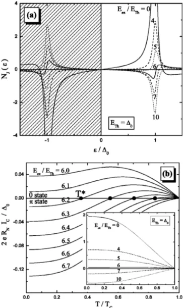
experi-mental situation. A short junction with ETh⬃⌬0 is therefore required to obtain a junction with a 0 – crossover in temperature. When the thickness is decreased, the energy spacing between the Andreev levels increases as shown from Eq.共2兲 for the bound states in ballistic regime: only one state remains at ⑀⫽⌬ for very short junctions. For the same rea-son the function NJ(⑀) in the diffusive regime has a peak around⑀⬃⌬. This peak comes from the first term in Eq. 共8兲 which does not contain the exchange energy because it de-scribes the superconductivity in the electrodes. The function NJ(⑀) in the S/F/S case is thus no more a shift of the S/N/S case as can be seen in Fig. 6共a兲 for increasing exchange energies. When the exchange energy and the Thouless energy
are of the same order, the large positive peak is replaced by a negative peak corresponding to a shifted Andreev spec-trum. The supercurrent becomes negative and the ground state is a state.
The temperature dependence of the critical current is plot-ted in Fig. 6共b兲 using an approximate expression ⌬(T)
⫽⌬0
冑
1⫺(T/Tc)2for the superconducting gap with the BCS relation ⌬0⫽1.76 kBTc. A state at zero temperature isobtained for exchange energies in the range
关6.2 ETh,31ETh兴, but a crossover to a 0 state in temperature is obtained only in the interval关6.2 ETh,6.5 ETh兴. This very narrow range of parameters illustrates the necessity to have an exchange energy as small as possible, at least comparable with the superconducting gap, in order to observe experi-mentally the crossover in temperature.
FIG. 6. 共a兲 Spectral supercurrent density for ⫽/2 at zero temperature in short junctions with ETh⫽⌬0and different exchange
energies Eex/ETh⫽0⫺10. 共b兲 Temperature dependence of the
criti-cal current in the range 6.0– 6.7共and 0–10 in the inset兲. The tem-perature induces a crossover between 0 and states only in the small range 6.2– 6.5.
D. Temperature-dependent exchange energy
In the above description the exchange energy was as-sumed to be a constant parameter. Its dependence with tem-perature can no more be neglected if the crossover occurs when the magnetization has not reached its saturation value
共if T* is not much smaller than TCurie). In this case the Andreev spectrum tends to move back towards the position for zero exchange energy when the temperature is increased and the negative critical current tends to become positive again. This effect suggested in Ref. 2 adds to the intrinsic 0 – crossover we described previously caused by the ther-mal distribution of quasiparticles.
We illustrate this effect in Fig. 7 by plotting the critical current versus temperature for different variations of the form Eex(T)⫽Eex(0)关1⫺(T/TCurie)␣兴1/␣. The value at zero temperature is fixed at Eex(0)⫽6.4ETh corresponding to a negative critical current for ETh⫽⌬0 and we choose TCurie
⫽3Tc typical for dilute ferromagnetic alloys. For ␣⫽100, the exchange energy is constant below Tc, so that the cross-over is induced by the thermal distribution function only. For
␣⫽2, the crossover occurs at lower temperature because the
two mechanisms are involved. For a faster decrease with␣
⫽1.3, the temperature dependence of the critical current is
almost dominated by the variations of the exchange energy. This additional effect can therefore contribute significantly to the 0 – crossover.
IV. EXPERIMENTAL STUDY OF NbÕCu52Ni48ÕNb JUNCTIONS
A. Description of the devices
We now present our experimental results on junctions which support the theoretical analysis of the previous part.
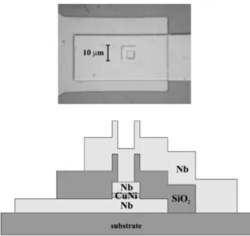
The crossover in temperature is easier to observe if the range of temperature is large共high superconducting transition tem-perature兲 and if the exchange energy is weak. So we chose niobium for the superconducting electrodes and a dilute copper-nickel alloy for the ferromagnet barrier. The first step of the process is to deposit the three layers Nb共100 nm兲/ CuNi共15–20 nm兲/Nb共100 nm兲 in situ in order to achieve a good quality of the interfaces. The patterning of the planar junctions is then made by photolithography. The bottom electrode is defined in this trilayer by a lift-off process and a square of 10⫻10m2 is then dry etched to define the junc-tion. The contact on the top is made with a Nb electrode through a window in a SiO2 layer共Fig. 8兲.
Nb and CuNi are sputtered using dc magnetron sources at room temperature in 1.64⫻10⫺2 mbar of argon gas. The re-sidual pressure inside the chamber is about 10⫺7 mbar. The deposition rates measured by glancing incidence x-ray re-flectometry and ␣-step measurements are 40 Å/s for Nb and 7 Å/s for CuNi in the center of the 75-mm wafer. The CuNi thickness was also determined at different positions on the substrate where several junctions are simultaneously pat-terned and we obtained a thickness range between 15 and 20 nm. The residual resistivity at 10 K for a thick niobium film is 8 ⍀ cm corresponding to a mean free path of 5 nm and the transition temperature is 8.7 K. The residual resistivity for copper-nickel films is 50⍀ cm corresponding to a mean free path about 1 nm and a diffusion coefficient of about 5 cm2/s共using parameters of copper兲. The actual com-position of the CuNi alloy was measured to be 48% of Ni by Rutherford backscattering on 5-nm and 10-nm films.
The magnetic properties of this Cu52Ni48 alloy have been measured using a superconductivity quantum interference device 共SQUID兲 magnetometer on a 20-nm film in a Nb/ CuNi/Nb trilayer and on a 200-nm film in a single CuNi layer. The temperature dependence of the magnetization is
FIG. 7. Crossover in temperature with the additional contribu-tion of a temperature-dependent exchange energy Eex(T) in a short
S/F/S junction with ETh⫽⌬0, Eex(0)⫽6.4 ⌬0, and TCurie⫽3 Tc.
Three different dependencies are compared: ␣⫽100, 2, and 1.3, corresponding to the increasing temperature variations shown in the inset.
FIG. 8. Photograph and cross section of a device: a square junc-tion of 10⫻10m2is etched in the Nb/Cu
52Ni48/Nb trilayer and
shown in Fig. 9 under parallel magnetic fields of 100 G and 200 G. The Curie temperature is about 35 K for the trilayer and 20 K for the single layer. The magnetic-field dependence of the magnetization at 5 K is shown in the inset of Fig. 9 for the 200-nm single layer. The saturation magnetization can be extrapolated to 50 emu/cm3which corresponds to a magnetic moment of 0.06B/atom. Bulk alloys of the same composi-tion have similar characteristics with a Curie temperature of 23 K and a magnetic moment of 0.041B/atom.28 The ex-change energy of bulk alloys has been calculated as a func-tion of the concentrafunc-tion between 100% and 70% of Ni共Ref. 29兲 and a linear extrapolation for 48% 共both the Curie tem-perature and the magnetic moment depend linearly on the concentration兲 indicates a value Eex⬇12 meV which is about ten times larger than the superconducting gap of nio-bium.
An important property of our Cu52Ni48 films is the
ab-sence of hysteresis, there is no measurable remanent magne-tization, the magnetic behavior is perfectly reversible. This property indicates a very weak ferromagnetism close to the superparamagnetic behavior that occurs at 45% of Ni in bulk alloys.28,30In this regime the magnetic correlations are not long range any more, the direction of the magnetization can vary spatially without domain wall and the total magnetic moment can freely adjust to zero when the external field is removed. The characteristic length of these magnetic fluctua-tions is a few hundred atoms, close to the superconducting coherence length and the thickness of the barrier, so that the exchange energy is just uniform on the size of the Andreev bound states which carry the supercurrent through the junc-tion.
B. Measurements of the critical current
The device is thermally coupled to the mixing chamber of a dilution refrigerator and electrically connected to a
care-fully filtered current source. The voltage between the super-conducting electrodes is measured with a very sensitive setup since the characteristic voltage is a few nanovolts. A small fraction of the bias current flows into a parallel circuit containing a known resistance of 80 m⍀ 共much larger than the resistance of the junction兲 and a SQUID sensor which measures the derived current. The voltage across the junction is simply the product of this current by the resistance.
First we present the results obtained on a junction with a CuNi thickness about 18 nm and then we will consider dif-ferent thicknesses. The voltage-current characteristic at 3.5 K is shown in the inset of Fig. 10 and is well described by the resistively shunted junction 共RSJ兲 model in agreement with the low resistance and low capacitance of the junction.31The normal resistance RN⫽1.6⫻10⫺4⍀ is close to the intrinsic CuNi layer resistance obtained from the resistivity and this indicates a good interface transparency. The critical current is measured continuously with a feedback method when tem-perature and magnetic field are varied. The temtem-perature de-pendence is shown in Fig. 10 and presents a very unusual behavior with a cancellation at T*⫽4.3 K where the
voltage-current characteristic is a straight line going through the origin. This behavior corresponds to the crossover dis-cussed extensively in the previous part with a sign in the current-phase relation that changes from negative at low tem-perature to positive above T*and leads to the corresponding change from a state to a 0 state.
The negative value of the critical current below T*cannot be measured using a single junction because the direction of the current is imposed by the current source. The direct de-termination of the sign requires a control of the phase differ-ence between the two superconducting electrodes and can be achieved by putting the junction in a superconducting
FIG. 9. Magnetization versus temperature for a 20-nm Cu52Ni48
layer in a Nb/CuNi/Nb trilayer and for a 200-nm Cu52Ni48single
layer. A magnetic field of 100 and 200 G is applied because the remanent magnetization is zero. Inset: reversible magnetization ver-sus magnetic field at 5 K for the 200-nm Cu52Ni48single layer.
FIG. 10. Critical current versus temperature for a Nb/Cu52Ni48/Nb junction with d⫽18 nm. The cancellation at T*
corresponds to a change of the critical current sign and therefore to a crossover between a 0 state and a state. Inset: voltage-current characteristic at 3.5 K 共the solid line is a fit using the RSJ model and the dashed line represents the normal resistance兲.
loop. This experiment was done by Ryazanov et al.7,8 who observed the same kind of temperature dependence in Nb/ CuNi/Nb junctions with higher Ni concentrations and hyster-etic magnetization curves. They placed five identical junc-tions in a double superconducting loop and observed an interference pattern shifted by half a flux quantum when the temperature is decreased below T*. This result demonstrates unambiguously that the sign of the current-phase relation changes at T* and is negative below. We will therefore call
state the temperature region below T* and 0 state the region above.
The magnetic-field dependence of the critical current is shown in Fig. 11 at three different temperatures below and above T*. These curves present only small distortions with respect to the ideal Fraunhofer diffraction pattern共inset兲 and are almost centered around zero magnetic field in agreement with the zero remanent magnetization observed by magnetic measurements. The periodicity is about 14 G and corre-sponds to an effective thickness d⫹2L⬇140 nm consistent with the London penetration depth of niobium. The position of these curves does not change with temperature, only the amplitude does, and the critical current at T* is zero for all values of the field. This result proves that the vanishing criti-cal current observed at T*in Fig. 10 is not due to a shift of the diffraction curve caused by an internal magnetic induc-tion. If it were the case a nonzero critical current should be recovered by adding an external magnetic field at T*. The crossover is indeed not due to a spatial distribution of super-current that compensates to zero at a given magnetic flux, but to a spectral distribution of supercurrent that compensates to zero at a given value of the exchange energy together with a given thermal distribution of quasiparticles.
The amplitude of the critical current and the shape of the
diffraction pattern always change between successive cool-ing and depend on the magnetic field present when the nio-bium becomes superconducting. The earth field and the bias current create vortices in the electrodes and the resulting in-homogeneous magnetic field distorts the diffraction patterns of the junction. However, the crossover temperature T* has always the same value because it is an intrinsic property which is independent of the magnetic field.
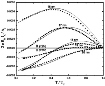
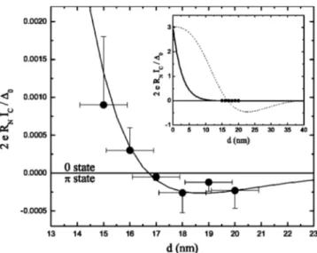
We compare now different junctions with CuNi thick-nesses between 16 and 20 nm and show in Fig. 12 the tem-perature dependence of their critical current plotted with a negative sign when the ground state is supposed to be. A crossover in temperature is obtained only for thicknesses be-tween 17 and 19 nm, thinner junctions are always in the 0 state and thicker junctions always in thestate. This behav-ior was expected and confirms that the 0 and states corspond, respectively, to the high- and low-temperature re-gions. When the thickness is small, the Thouless energy is large and the exchange energy becomes insufficient to shift the Andreev spectrum, so the ground state is the usual 0 state. The 16 nm junction behaves however differently from an usual Josephson junction since the critical current has a maximum at finite temperature. This indicates the presence of a negative supercurrent density which is close to the Fermi level and is suppressed when the temperature in-creases. The 20-nm junction has no crossover but the curva-ture of its critical current close to Tc is also unusual com-pared to the linear behavior of short junctions. This temperature dependence results from the combined effect of the superconducting gap that closes at Tcand a crossover to a 0 state that would have occurred at a temperature just above Tc.
FIG. 11. Critical current versus magnetic field for a Nb/Cu52Ni48/Nb junction with d⫽18 nm. These curves do not
move with temperature and the critical current disappears com-pletely共for all fields兲 at the crossover temperature of 4.3 K. Inset: comparison with the ideal Fraunhofer diffraction pattern 共solid line兲.
FIG. 12. Critical current versus temperature for Nb/Cu52Ni48/Nb junctions with d⫽16–20 nm. The critical current
is normalized and plotted with a negative sign for the ground states. The solid lines are the theoretical curves obtained for each thickness by adjusting the exchange energy and the spin-flip length 共Sec. V B兲 in order to fit the experimental data. Eex(0) was found in
V. COMPARISON WITH THE THEORETICAL MODEL A. Discussion of the temperature dependence
First we consider the 18-nm junction and try to reproduce its temperature behavior with a crossover at T*⫽4.3 K using
the theoretical model of Sec. III. Three parameters are known: the normal resistance RN⫽1.6⫻10⫺4 ⍀, the Thou-less energy ETh⫽1 meV, and the superconducting gap ⌬0
⫽1.3 meV. The experimental critical current is plotted in
Fig. 13 together with the theoretical curve using a constant exchange energy Eex⫽6.4 meV 共dotted line兲. Both are ex-pressed in terms of the normalized parameter 2eRNIC/⌬0
but the amplitude of the theoretical curve has been strongly reduced to be comparable with the experimental one: the origin of this extremely weak supercurrent will be analyzed in the following section.
The saturation at low temperature is a general behavior: it occurs below about 0.2 Tcfor short junctions and below the Thouless energy for long S/N/S junctions. However, this saturation is not共or much less兲 present in our S/F/S junction because the exchange energy is still temperature dependent at low temperature. This dependence was reported for bulk CuNi alloys32and our own magnetic measurements共Fig. 9兲 also show that the magnetization is not saturated at 5 K and is still increasing linearly. For this reason we consider now the model already discussed in Sec. III with a temperature-dependent exchange energy Eex(T). Using a linear depen-dence and a Curie temperature of 35 K, this model repro-duces better the experimental behavior at low temperature.
The different types of curves measured for different CuNi thicknesses can be reproduced with an exchange energy at zero temperature of about 7 meV 共Fig. 12兲 using the same linear dependence for Eex(T) as before. As already men-tioned, the theoretical amplitudes have to be strongly
re-duced to fit the experimental data: the physical origin of this reduction is explained in the following.
B. Discussion of the critical current amplitude
The large discrepancy between the measured amplitude and the model cannot be explained by the interface transpar-ency because the barrier parameter ⌫b⫽0.3, deduced from the normal resistance RN⫽1.6⫻10⫺4 ⍀⫽(1⫹2⌫b)d/S, is too small to have such an influence.25 This good interface quality is achieved by an in situ deposition of the Nb/ CuNi/Nb trilayer which avoids any contamination of the in-terface. Moreover, the small spin polarization of this very dilute magnetic alloy cannot reduce significantly the prob-ability of the Andreev reflection as it is expected to do with high Curie temperature ferromagnets where the densities of states per spin are not equal.33
In the theoretical model we neglected any inelastic and decoherent process because the typical thickness of S/F/S junctions is usually quite small. However, our CuNi alloy has a superparamagnetic behavior which indicates that the mag-netic moments can fluctuate easily and induce a large spin-flip scattering. This process destroys a large number of An-dreev pairs and reduces therefore the supercurrent amplitude. However, the surviving pairs still form bound states whose spectrum depends on the exchange energy and the state is not destroyed.
This process can be qualitatively taken into account by simply adding an exponential decay exp(⫺d/Lsf) with a spin-flip scattering length Ls f. The maximum critical current at zero temperature is plotted in Fig. 14 as a function of the thickness and is well reproduced by the model with Eex
⫽7.2 meV and Ls f⫽2.7 nm. The error bars on the critical current indicate that higher values may be possible since we observed some changes depending on cooling conditions
共see Sec. IV兲 typically by a factor of 2. The very small value
FIG. 13. Temperature dependence of the critical current for d ⫽18 nm 共normalized and plotted with a negative sign below the crossover兲 compared with the theoretical model with a constant 共dotted line兲 or temperature dependent 共solid line兲 exchange energy as shown in the inset. The spin-flip scattering共Sec. V B兲 has been included with Ls f⫽3.1 nm 共dotted line兲 and 2.6 nm 共solid line兲.
FIG. 14. Critical current of Nb/Cu52Ni48/Nb junctions at zero
temperature versus CuNi thickness compared to the theoretical model with Eex(0)⫽7.2 meV and a spin-flip length Ls f⫽2.7 nm
共solid line兲. Inset: same graph on a larger scale, plus the theoretical curve without spin-flip scattering共dashed line兲.
obtained for the spin-flip length can be compared to the 7.5 nm measured in the Cu77Ni23alloy which is not magnetic at
all, only because of the spin-orbit coupling.34 It is therefore not unrealistic to have a shorter value in our superparamag-netic alloy.
The spin-flip scattering can also be directly included in the equations and this can be done easily in the linearized case by changing ⑀ into ⑀⫹i␥s f in the second term of Eq.
共10兲, but not in the term containing the gap where ␥⫽0⫹.
This new theoretical expression reproduces the experimental data with almost the same spin-flip length Ls f⫽
冑
បD/␥s f⫽2.5 nm. However, it requires a different exchange energy
Eex⫽20 meV because the shift of the Andreev bound states is now intrinsically coupled to the spin-flip scattering pro-cess.
VI. CONCLUSION
We have explained the state of S/F/S junctions by a shift of the Andreev bound states in order to provide a better
insight into the microscopic mechanism of this effect. The spectral supercurrent density in the diffusive regime has been calculated and used to interpret the origin of the 0 – cross-over in temperature. We have presented some critical current measurements of Nb/Cu52Ni48/Nb junctions where the
bar-rier has a superparamagnetic behavior. In a small range of barrier thickness the critical current cancels out as a function of temperature when the ground state changes from 0 state to a state. Our theoretical model can reproduce these experi-mental results by including a temperature-dependent ex-change energy and a large spin-flip scattering.
ACKNOWLEDGMENTS
We thank A. Buzdin, M. Aprili, M. Houzet, I. Baladie´, A. Vedyayev, and V. Mineev for stimulating discussions and D. Jalabert for RBS measurements.
*Present address: Department of Nanoscience, Delft University of Technology, Lorentzweg 1, 2628 CJ Delft, The Netherlands.
1L.N. Bulaevski, V.V. Kuzi, and A.A. Sobyanin, Pis’ma Zh.
Eksp. Teor. Fiz. 25, 314共1977兲 关JETP Lett. 25, 290 共1977兲兴.
2A.I. Buzdin, L.N. Bulaevski, and S.V. Panyukov, Pis’ma Zh.
Eksp. Teor. Fiz. 35, 147共1982兲 关JETP Lett. 35, 178 共1982兲兴.
3A.I. Buzdin and M.Y. Kupriyanov, Pis’ma Zh. Eksp. Teor. Fiz. 53,
308共1991兲 关JETP Lett. 53, 321 共1991兲兴.
4H.K. Wong, B.Y. Jin, H.Q. Yang, J.B. Ketterson, and J.E. Hilliard,
J. Low Temp. Phys. 63, 307共1986兲.
5
J.S. Jiang, D. Davidovic´, D.H. Reich, and C.L. Chien, Phys. Rev. Lett. 74, 314共1995兲.
6T. Mu¨hge, N.N. Garif’yanov, Y.V. Goryunov, G.G. Khaliullin,
L.R. Tagirov, K. Westerholt, I.A. Garifullin, and H. Zabel, Phys. Rev. Lett. 77, 1857共1996兲.
7V.V. Ryazanov, V.A. Oboznov, A.Y. Rusanov, A.V. Veretennikov,
A.A. Golubov, and J. Aarts, Phys. Rev. Lett. 86, 2427共2001兲.
8V.V. Ryazanov, V.A. Oboznov, A.V. Veretennikov, and A.Y.
Ru-sanov, Phys. Rev. B 65, 020501共2001兲.
9T. Kontos, M. Aprili, J. Lesueur, F. Geneˆt, B. Stephanidis, and R.
Boursier, Phys. Rev. Lett. 89, 137007共2002兲.
10W. Guichard, M. Aprili, O. Bourgeois, T. Kontos, J. Lesueur, and
P. Gandit, Phys. Rev. Lett. 90, 167001共2003兲.
11I.O. Kulik, Zh. Eksp. Teor. Fiz. 57, 1745共1969兲 关Sov. Phys. JETP 30, 944共1970兲兴.
12F.K. Wilhelm, G. Scho¨n, and A.D. Zaikin, Phys. Rev. Lett. 81,
1682共1998兲.
13T.T. Heikkila¨, F.K. Wilhelm, and G. Scho¨n, Europhys. Lett. 51,
434共2000兲.
14J. Bardeen, L.N. Cooper, and J.R. Schrieffer, Phys. Rev. 108,
1175共1957兲.
15M. Tinkham, Introduction to Superconductivity, 2nd ed. 共McGraw-Hill, New York, 1996兲.
16A.F. Andreev, Zh. Eksp. Teor. Fiz. 46, 1823共1964兲 关Sov. Phys.
JETP 19, 1228共1964兲兴.
17E.A. Demler, G.B. Arnold, and M.R. Beasley, Phys. Rev. B 55,
15 174共1997兲.
18A.F. Andreev, Zh. Eksp. Teor. Fiz. 49, 655共1965兲 关Sov. Phys.
JETP 22, 455共1966兲兴.
19C. Ishii, Prog. Theor. Phys. 44, 1525共1970兲.
20J. Bardeen and J.L. Johnson, Phys. Rev. B 5, 72共1972兲. 21A. Furusaki and M. Tsukada, Phys. Rev. B 43, 10 164共1991兲. 22T. Kontos, M. Aprili, J. Lesueur, and X. Grison, Phys. Rev. Lett.
86, 304共2001兲.
23S.K. Yip, Phys. Rev. B 58, 5803共1998兲. 24K.D. Usadel, Phys. Rev. Lett. 25, 507共1970兲.
25M.Y. Kupriyanov and V.F. Lukichev, Zh. Eksp. Teor. Fiz. 94, 139 共1988兲 关Sov. Phys. JETP 67, 1163 共1988兲兴.
26J.J.A. Baselmans, A.F. Morpurgo, B.J. van Wees, and T.M.
Klap-wijk, Nature共London兲 397, 43 共1999兲.
27V.V. Ryazanov, V.A. Oboznov, A.V. Veretennikov, A.Y. Rusanov,
A.A. Golubov, and J. Aarts, Usp. Fiz. Nauk 171, 81共2001兲.
28T.J. Hicks, B. Rainford, J.S. Kouvel, G.G. Low, and J.B. Comly,
Phys. Rev. Lett. 22, 531共1969兲.
29F. Brouers, A.V. Vedyayev, and M. Giorgino, Phys. Rev. B 7, 380 共1973兲.
30
J.P. Perrier, B. Tissier, and R. Tournier, Phys. Rev. Lett. 24, 313
共1970兲.
31K.K. Likharev, Rev. Mod. Phys. 51, 101共1979兲.
32S.A. Ahern, M.J.C. Martin, and W. Sucksmith, Proc. R. Soc.
Lon-don, Ser. A 248, 145共1958兲.
33M.J.M. de Jong and C.W.J. Beenakker, Phys. Rev. Lett. 74, 1657 共1995兲.
34S.-Y. Hsu, P. Holody, R. Loloee, J.M. Rittner, W.P. Pratt, and P.A.