HAL Id: hal-03023829
https://hal.archives-ouvertes.fr/hal-03023829
Submitted on 25 Nov 2020
HAL is a multi-disciplinary open access
archive for the deposit and dissemination of
sci-entific research documents, whether they are
pub-lished or not. The documents may come from
teaching and research institutions in France or
abroad, or from public or private research centers.
L’archive ouverte pluridisciplinaire HAL, est
destinée au dépôt et à la diffusion de documents
scientifiques de niveau recherche, publiés ou non,
émanant des établissements d’enseignement et de
recherche français ou étrangers, des laboratoires
publics ou privés.
Semipolar (10-11) GaN growth on silicon-oninsulator
substrates: Defect reduction and meltback etching
suppression
Rami Mantach, P Vennéguès, J Zuniga Perez, P de Mierry, M Leroux, M
Portail, G Feuillet
To cite this version:
Rami Mantach, P Vennéguès, J Zuniga Perez, P de Mierry, M Leroux, et al.. Semipolar (10-11) GaN
growth on silicon-oninsulator substrates: Defect reduction and meltback etching suppression. Journal
of Applied Physics, American Institute of Physics, 2019, �10.1063/1.5067375�. �hal-03023829�
meltback etching suppression
Cite as: J. Appl. Phys. 125, 035703 (2019); https://doi.org/10.1063/1.5067375
Submitted: 17 October 2018 . Accepted: 01 January 2019 . Published Online: 16 January 2019
Rami Mantach , P. Vennéguès, J. Zuniga Perez , P. De Mierry, M. Leroux, M. Portail, and G. Feuillet
ARTICLES YOU MAY BE INTERESTED IN
Study of deep traps in AlGaN/GaN high-electron mobility transistors by electrical
characterization and simulation
Journal of Applied Physics
125, 035702 (2019);
https://doi.org/10.1063/1.5055926
The role of transient surface morphology on composition control in AlGaN layers and wells
Applied Physics Letters
114, 031602 (2019);
https://doi.org/10.1063/1.5063933
Methodology for the investigation of threading dislocations as a source of vertical leakage
in AlGaN/GaN-HEMT heterostructures for power devices
Semipolar (10-11) GaN growth on
silicon-on-insulator substrates: Defect reduction
and meltback etching suppression
Cite as: J. Appl. Phys. 125, 035703 (2019);doi: 10.1063/1.5067375
View Online Export Citation CrossMark
Submitted: 17 October 2018 · Accepted: 1 January 2019 · Published Online: 16 January 2019
Rami Mantach,1,2 P. Vennéguès,1J. Zuniga Perez,1 P. De Mierry,1M. Leroux,1M. Portail,1and G. Feuillet2
AFFILIATIONS
1CNRS, Université Côte d’Azur, CRHEA rue Bernard Grégory, 06560 Valbonne, France 2CEA-LETI, MINATEC Campus, 17 rue des Martyrs, 38054 Grenoble, France
ABSTRACT
We demonstrate the growth of almost strain-free (10-11) semipolar GaN on silicon-on-insulator (SOI) substrates, with no melt-back etching and with a defect density strongly reduced compared to semipolar templates grown on patterned silicon sub-strates. This is carried out using SOI substrates with a very thin (∼150 nm) 6° off (001) Si top layer. By resorting to very small nucleation (111) facets, revealed through chemical etching of the topmost thin Si layer, we are able to diminish significantly the overall dislocation density. Cathodoluminescence and scanning electron microscopy images at different stages of the growth illustrate how the defect density reduction operates and confirm the complete suppression of meltback etching over the whole 2 in. wafer. Low temperature photoluminescence and optical reflectivity indicate that complete strain relaxation is closely achieved (D0X at 3.473 ± 0.001 eV), compared to semipolar epilayers grown onto“bulk” silicon (D0X at 3.460 eV). Thanks to this efficient strain relaxation, very thick layers, up to 9 μm, could be obtained crack-free.
Published under license by AIP Publishing.https://doi.org/10.1063/1.5067375
INTRODUCTION
Gallium nitride based materials are known for their excep-tional luminescence efficiency in the visible range, leading the race for the lighting device revolution.1,2However, GaN layers
and heterostructures are usually grown along the polar direc-tion (c-axis of the wurtzite structure), which results in internal polarizationfields.3These lead to an increase of the radiative
lifetime4that, if combined with a large density of non-radiative
defects, contributes to reducing the quantum efficiency and lifetime of devices.5
Semipolar and non-polar nitride materials have become a topic of interest because of their capability of reducing or even eliminating the effect of this internal polarizationfield6and, on the other hand, possibly enhancing indium incorporation.7 Semipolar samples can be homo-epitaxially grown on semipolar GaN wafers resulting in very low dislocation densities,8down to
105to 104cm−2, as demonstrated by Fujito et al.9However, the semipolar wafers are still of very small sizes and rare, hence explaining the interest in heteroepitaxial semipolar GaN.
Several attempts for growing semipolar GaN directly on foreign substrates have been performed. However, they often
resulted in poor quality epilayers with very large disloca-tion and basal stacking fault (BSF) densities (1010cm−2and
105cm−1, respectively).10 In situ low temperature (LT)-AlN
interlayers have been used to block basal stacking faults (BSFs), but this method is not always efficient, particularly on semipolar orientations with high inclination angles with respect to the c-axis.11 Hence, there is a clear interest in finding a way that leads to low dislocation and BSF densities in heteroepitaxial semipolar layers.
Honda et al. were thefirst to grow semipolar (10-11) GaN on patterned substrates. In their approach, the growth takes place on inclined v-shaped (111) facets etched on the silicon substrate,12the inclination of which determines the orientation
of the GaN semipolar epilayer grown thereon. Accordingly, various semipolar orientations were achieved, including (11-22) GaN layer on the r-plane patterned sapphire substrate (PSS),13,14(11-22) GaN on the patterned (113) Si substrate,15and
(20-21) GaN on the (114) 1° off patterned Si substrate.16
In the case of sapphire substrates, several methods have been implemented to reduce the dislocation density in the semipolar GaN layers; in particular, the so-called 3-steps
Journal of
Applied Physics
ARTICLE scitation.org/journal/japJ. Appl. Phys. 125, 035703 (2019); doi: 10.1063/1.5067375 125, 035703-1
density in the mid-107cm2range and a BSF density of around 100 cm−1, establishing the current state of the art. (20-21) semipolar GaN and InGaN quantum well were also demon-strated on similarly patterned sapphire substrates.17Recently, semipolar (11-22) 550 nm yellow/green18 and 444 nm blue InGaN light-emitting diodes (LEDs)19 and semipolar (20-21)
GaN and InGaN LEDs20were demonstrated on sapphire
tem-plates using this defectfiltering method.
Growth is more challenging on patterned silicon sub-strates, among other reasons due to the meltback etching problem: a reaction between Si and Ga that initiates during growth and results in a violent outspread of matter causing complete destruction of the sample surface.21 Yu et al. suc-ceeded to grow semipolar (20-21) GaN on stripe patterned (113) Si with no meltback etching.15 Khoury et al. eliminated
the reaction by adding a small amount of N2to the carrier gas
during the growth, but at the expense of negatively affecting the coalesced GaN quality by increasing the number of gener-ated structural defects. The state of the art for the dislocation density in semipolar GaN grown on patterned silicon sub-strate is 2.7 × 108cm−2.22
In the work reported here, we demonstrate the growth of (10-11) GaN layers grown on patterned (001) 6° off silicon-on-insulator (SOI) substrates that allow to further reduce the dislocation density and eliminate meltback etching. Following KOH etching of the thin enough (see later) top Si layer, growth takes place on very small Si inclined facets. This is the key to reducing the defect density, which relies on dislocation bending in pyramidal grains as explained by Vennéguès et al.23 The combination of small nucleation
facets and, therefore, of small pyramids results in the con-finement of the emerging dislocations in a very narrow zone of the layer surface. These regions are surrounded by almost dislocation free areas.13,23Both the width of the region
con-taining the threading dislocations and the number of nucle-ated dislocations depend on the facet size, pinpointing the importance of SOI substrates. We also show that another important advantage related to using SOI substrates and small growth facets is the elimination of the meltback etching, aided by the strong reduction of the interaction surface between Ga and Si.
EXPERIMENTAL METHOD
Unlike standard patterned bulk Si substrate, our sub-strate is an SOI wafer composed of a top (001) 6° off Si layer whose thickness determines the size of the Si growth facet. For this work, the top Si layer is 150 nm thick, while the SiO2
layer, present between the two Si layers, has a thickness of 500 nm. The bottom Si substrate is <001> oriented with a thickness of 500μm.
Patterning
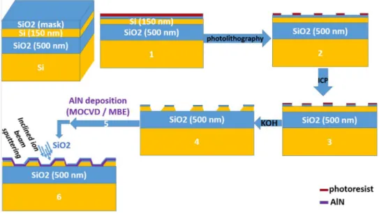
The successive patterning steps are depicted in Fig. 1. Thefirst step is the deposition of a 50 nm thick SiO2mask on
the top Si using ion beam sputtering (IBS) (Fig. 1, step 1). The
defined using standard photolithography with a 5 μm period (2.5μm opening and 2.5 μm mask) (Fig. 1, step 2). The aper-tures of the SiO2 masks are dry etched using an inductively
coupled plasma (Fig. 1, step 3). The sample is then cleaned for 30 s in a buffered oxide etch (BOE) to eliminate the native oxide, which often prevents KOH from etching silicon.
The substrate is then exposed to wet etching using KOH, revealing (111) and (11 1) opposite facets. In our case, these facets have an inclination of 48° and 60°, respectively, with respect to the 6° off (001) top Si surface (Fig. 1, step 4). If we would have used patterned Si substrates instead of SOI, etching would have stopped automatically once a complete “V” shape groove was formed. This would have resulted in two large (2–3 μm wide) opposing {111} Si facets,16 whose size
would have determined the defect density. Besides, the homogeneity of KOH etching was reported to be poor for bulk Si substrates;22 this is due to the random initiation of KOH etching because of the thickness non-uniformity of the native silicon oxide layer on the silicon surface. Therefore, locally retarded etching may yield different Si facet sizes, making coalescence of neighboring bands/grains random. To achieve a perfect uniformity of the facet sizes over the whole substrate surface, we used SOI substrates. Indeed, the top Si layer can be totally etched, the SiO2layer just below acting as
a perfect etch-stop. The thickness homogeneity for the top Si layer of the SOI substrate was measured by reflectometry and found to be better than ±2% on a 2-in. wafer, therefore yield-ing very homogeneous facet heights.
Subsequently, a 50 nm thick AlN layer is grown (Fig. 1, step 5) at 1210 °C using a Metal-Organic Vapor Phase Epitaxy (MOVPE) vertical close coupled shower head reactor.24
Growing AlN on the Si surface is a prerequisite to avoid melt-back etching from occurring through the direct contact between Ga and Si. The used metal precursor is trimethylalu-minum and the temperature is measured using an in situ thermocouple below the susceptor pockets where the sub-strates are placed.
Thefinal step consists in the inclined deposition of SiO2
(Fig. 1, step 6) using IBS. This is done in order to cover the top surfaces but also the {111} 48° inclined facets while avoiding any deposition on the 60° inclined facet, where GaN growth needs to be initiated.Figure 2 is a scanning electron micro-scope (SEM) cross-sectional image of thefinal patterned SOI surface (the 50 nm-thick AlN seed layer is hard to visualize at such a magnification).
Growth
The same MOVPE reactor as the one for AlN deposition was used for the selective growth of GaN. The precursors were trimethylgallium (TMGa) and ammonia (NH3). The
growth process was divided into two steps: thefirst one is the growth of GaN pyramids at 1090 °C, high pressure (300 Torr), and a V/III ratio of 1500. In a second step, in order to achieve coalescence, growth is continued at the same temperature but lower pressure (100 Torr) and lower V/III ratio (650). It is
worth mentioning that using the same growth parameters as for the GaN pyramids on large Si growth facets (as obtained when using the bulk Si substrate) results in parasitic growth: indeed, GaN islands are nucleated on the entire surface (i.e., also on the SiO2 mask) and lead to the formation of
incomplete GaN pyramids on the growth facets. Therefore, pressure, TMGa, and NH3 fluxes should be adjusted for the
nucleation and growth onto small facets. This can be under-stood by considering that the growth on the facet is related to two adatoms fluxes: one from direct deposition and the other from species diffusion on the mask from either side of the growth facet. If the growth conditions employed for small facets are identical to those used for large facets (TMGa fluxes of 2200 instead of 1600 μmol/min), the reservoir of species available for growth is too high, eventually leading to parasitic deposition on the SiO2mask from either side of the
small facet. This explains the necessary growth adjustments when going from large to small facet sizes.
RESULTS AND DISCUSSION
Figure 3(a)shows the formation of perfect GaN pyramids after 500 s of growth at 300 Torr using 3.5 slm NH3. The aim
is to create a pyramid at the beginning of growth in order to bend all dislocations nucleating on the inclined Si facets.13,19 This growth stage is referred to as stage A. Continuing growth under the same condition for 1500 s leads to the formation of small c facets as shown inFig. 3(b)(stage B). At this particular moment, the growth parameters are changed in order to favor the growth in the +c direction for reaching coalescence: the pressure is decreased to 100 Torr and the ammoniaflow to 1.5 slm, keeping the TMGaflow constant.
Appropriately splitting the growth time between the 2 steps enables fast coalescence for the formation of a continu-ous GaN layer. Figures 3(c) and3(d) show a coalesced layer for a growth duration of 8000 s (overall time) which resulted in a 7μm-thick crack free GaN (10-11) epilayer (stage C).
The first important result is that, contrary to the case where bulk Si substrates are used for growing semipolar GaN, no meltback etching was detected on the surface of the sample. This is achieved without having to use methods such as, for instance, that reported in Ref.21, where an N2flow was
added to the H2 carrier gas. In the case of c-oriented
two-dimensional GaN growth, the use of an AlN buffer layer is suf-ficient for avoiding melt back etching, without having to resort to reducing the substrate footprint. For semipolar nitrides, things are a lot different since patterning the Si sub-strate seems to have a great influence on melt-back etching. The reason for the different behaviors is not clear at present. But one may assume that it can be related to the way the (111) Si surface is prepared. Indeed, KOH etching used here for defining {111} facets may leave either a much more reactive
FIG. 1. Patterning steps of SOI. 1, photoresist deposition; 2, photolithography; 3, SiO2dry etching; 4, SOI wet etching; 5, AlN deposition; 6, SiO2deposition using an
inclined beam sputtering.
FIG. 2. A cross-sectional SEM image for the SOI substrate after patterning. Growth facet and SiO2mask are shown.
Journal of
Applied Physics
ARTICLE scitation.org/journal/japJ. Appl. Phys. 125, 035703 (2019); doi: 10.1063/1.5067375 125, 035703-3
surface with respect to Ga/Si interactions than in the case of surfaces obtained by chemical-mechanical polishing (CMP); furthermore, KOH etching may leave surface imperfections (steps, macrosteps, impurity clusters) inducing AlN thickness irregularities, through which Ga diffusion may be favored. If this were the case, reducing the Si footprint for growth reduces the probability for encountering such surface imper-fections. A second reason might be related to the different etching times required to reveal the growth facets, which are much shorter in the current work. Indeed, since at room-temperature the (100)/(111) etching rate ratio amounts to about 100, if during the KOH etching the {111} facets form steps, the anisotropic etching ratio might lead to the forma-tion of surface pits that, once again, might enhance the melt-back etching probability. Thus, in the present case of semipolar growth on etched {111} Si facets, the AlN layer alone cannot do the job by itself, as shown in Refs.16and21, where meltback occurred despite the use of an AlN buffer layer. Hence, the advantage of using a smaller substrate footprint.
Cathodoluminescence (CL) was carried out in a JEOL 7000F scanning electron microscope (SEM) equipped with a Gatan Mono CL4 module. CL images were used in order to locate the defects, mainly dislocations and basal stacking faults (BSFs) in the layers at the different stages of growth (A: pyramid nucleation, B: pyramid lateral extension leading to continuous stripes, and C: completely coalesced layer). Threading dislocations are non-radiative centers and as such
appear as dark spots on panchromatic CL images. Most mea-surements have been done at 77 K, allowing us to detect the presence of BSFs, which act as radiative centers with associ-ated levels in the gap, relatively close to the band edge, hence being difficult to detect at room temperature (RT).25Figure 4
shows the 77 K panchromatic CL images of samples at the three stages of growth (A, B, and C). After stage A [Fig. 4(a)], corresponding to pyramid nucleation, a non-radiative spotty line, presumably associated to dislocations coming from the growth facet, can be seen (red arrows) and appears over a very limited width. Within the bands inFigs. 4(a) and 4(b), bright and dark regions with triangular shape are present as well. These are related to the overlapping of adjacent pyra-mids that, upon coalescence in the direction of the bands, have left some underlying voids between them [as observed in cross-sectional SEM images; see Figs. 3(c) and 3(d)]. Dislocations are not seen anywhere else. After stage B [Fig. 4(b)], complete GaN stripes were formed and no addi-tional dislocations are seen. It is noteworthy that BSFs are not created unless growth parameters are changed. Indeed, they start to be created while growing in the –c direction before complete coalescence occurs. Besides, the coales-cence of the bands from adjacent stripes is accompanied too by the occurrence of basal stacking faults, as evidenced from their luminescence [Fig. 4(c)].
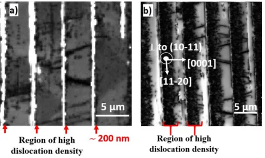
Most interestingly, the CL images in Fig. 5(a), taken from the top of the layers, reveal that the width of the high
dislocation density regions is limited to 200–300 nm in fully coalesced layers [Fig. 5(a)]. For comparison, in the case of large facets [Fig. 5(b)],22as obtained for semipolar growth on bulk 7° off (001) Si substrates, the typical width of the emerg-ing dislocation area is around 4μm for {111} 4–5 μm large Si facet. This highlights the second advantage brought about by the use of patterned thin SOI in terms of dislocation reduc-tion. From simple geometrical considerations, one can deduce the width of the dislocation zone at the surface of the semipo-lar sample. As already discussed, dislocations originate at the Si/AlN interface and propagate along the c direction. Upon intersecting one of the GaN pyramid facets, these dislocations bend in the c-plane either upward or downward, in order to minimize their elastic energy (Fig. 6). Therefore, emerging dis-locations are confined in a region of the surface (of width W) situated above the nucleation facet. The last dislocation to be bent is the one closest to the pyramid apex. This determines the width W of the large density dislocation region on the surface, which is simply the projection of the pyramid facet on the layer’s surface. In our case, because the facet is inclined at 60° to the surface, we infer a width of the dislocated zone W = H/sin 60, with H being the thickness of the top Si layer of the SOI. H = 150 nm, hence W∼ 175 nm in fairly good
agreement with the experimental width. Outside this narrow dislocated region, the dislocation density crossing the rest of the surface is approximatively 4 × 107cm−2. All in all, and taking the bent dislocations into account, the dislocation density was calculated using room temperature CL images where BSFs are not seen and was found to be about 108cm−2.
Other dark lines inclined at 75° to the11–20direction can also be seen, as evidenced inFig. 5(a), corresponding to dislo-cations, or clusters of dislodislo-cations, appearing only after coa-lescence has occurred between neighboring stripes. These dislocations are presumably generated by the relaxation of the strained GaN layer through dislocation glide in the pris-matic m-plane, as expected in semipolar GaN.26
Now, concerning BSFs, they start forming when the GaN pyramids begin over-growing the SiO2mask in the–c direction.
Growth rate in the +c direction is much faster than in the–c direction, the ratio being as large as 7 during epitaxial-lateral-overgrowth experiments.27 Indeed, it is believed that lower
growth rates result in higher impurity incorporation, leading to enhanced formation of stacking faults, hence higher BSFs density in the–c direction compared to the +c one.28The
pan-chromatic images inFigs. 4(a)and4(b)show that no BSFs are formed before changing the growth parameters in order to
FIG. 4. Cathodoluminescence images (77 K) for the pyramids nucleation (a), for the pyramids coalescence (b), and for the strips coalescence (c). Dislocations are shown as black dots and lines; BSFs are the bright lines.
Journal of
Applied Physics
ARTICLE scitation.org/journal/japJ. Appl. Phys. 125, 035703 (2019); doi: 10.1063/1.5067375 125, 035703-5
favor the coalescence of the stripes. This is mainly due to the fact that the growth parameters employed during the first growth step fully favor growth along +c and, thus, GaN does not grow in the–c direction even if the pyramids size is much larger than the Si facet size. On the other hand, the growth conditions in the second step favor two-dimensional growth and result in some–c growth. InFig. 4(c), where the growth is complete, BSF (bright lines) and dislocations (black lines) appear with the periodicity of the underlying Si facets. The
density of BSFs was estimated from the CL images. Our count-ing procedure consists in acquircount-ing CL images 10μm × 10 μm large, summing the length of bright lines and dividing it by the image surface (100μm2). This gives a density of bright lines in
the order of 3–4 × 103cm−1. Assuming a density of 10 BSFs/
100 nm in the regions of bright lines, as previously measured by TEM,29we can estimate a BSFs density in the low 105cm−1
(high 104cm−1). Contrarily, for semipolar GaN grown on bulk Si
substrates employing a one-step growth, GaN pyramids are
FIG. 5. High dislocation density region in the case of GaN on SOI (77 K) (a) and on Si bulk substrates (300 K) (b).
free to overgrow the SiO2mask in the–c direction, leading to
the formation of a larger number of BSFs. Our study consists in growing GaN in two growth steps, allowing for a better control of growth in the–c direction. Indeed and as evidenced inFig. 3, the BSFs are absent in the individual pyramids and in the bands before changing the growth parameters in order to achieve coalescence. The photoluminescence (PL) spectra (shown later inFig. 7) illustrate the difference between the BSF related intensity of semipolar GaN on bulk Si and SOI sub-strates, which is coherent with the reduced density of BSFs extracted from our CL study.
Photoluminescence (PL) was used not only to probe the optical quality of the semipolar (10-11) epilayers but also for investigating defects, essentially BSFs. PL measurements were carried out at 15 K.Figure 7compares the PL spectra of two different semipolar samples with the same (10-11) orientation: on patterned SOI (black line) and on patterned bulk Si (red line). The PL bands near 3.405 eV involve I1 basal stacking
faults. Hence,Fig. 7evidences a strong reduction of their rela-tive contributions in the case of the sample grown on SOI, corresponding to a reduced density. This is consistent with the CL observations discussed above. As it is well known, the position of the near band edge luminescence is closely related to the strain. While the donor bound exciton (D0X) of
semipo-lar GaN on bulk Si emits at 3.460 eV, indicative of a tensile strain (in relaxed GaN, the energy of excitons bound to the residual donors Si or O is 3.471–3.472 eV), in the sample on SOI its energy is 3.473 eV. Rather than indicating a compressive strain, this emission energy points toward the presence of a second emission contribution, which corresponds to free-exciton emission. Indeed, 15 K reflectivity spectrum, also shown in Fig. 7(blue line), shows a free excitonic feature at 3.475 ± 0.001 eV, confirming a much lower tensile strain than on Si substrates, but not a compressive strain (the energy of A
excitons is 3.477–3.478 eV in relaxed GaN). Interestingly, as was apparent inFig. 5(a), a crack can be detected, synonymous of the relaxation of a residual tensile stress in the layers: the semipolar layers are very close to full relaxation but still subject to a very small residual tensile stress explaining why there are very few cracks, even for 8–9 μm GaN thicknesses. In fact, most of the surface is crack-free, as seen for instance in
Figs. 3(d)and4(c).
The mechanism beyond this almost full relaxation is not well understood yet. GaN pyramids and stripes (i.e., before coalescence) may relax elastically due to available free sur-faces at sufficiently close distances (at most 2.5 μm away). For coalescedfilms, one hypothesis would be that the stress is transferred from the thick (8–9 μm) GaN layer to the thin (150 nm) and non-continuous top Si layer, which shouldfind itself deformed. We are currently working to assess this hypothesis. Still, one should note that the exciton energy reveals that there exists a residual, albeit very small, tensile strain in the coalesced layer. This very small tensile stress explains why there are almost no cracks, even for 8–9 μm GaN thicknesses. A study of strain evolution as growth pro-ceeds will be reported later.
The absence of stress in semipolar heterostructures when grown on SOI is of course very important, as it will allow us to design, for instance, optimal LED structures not requiring strain-compensating layers.
CONCLUSION
We have demonstrated the growth of (10-11) GaN on SOI substrates on which we have fabricated nanometric facets, 150 nm wide. This specific substrate structure and this thin Si top layer have been used to reduce the dislocation density in GaN, given that it is essentially determined by the footprint of GaN on the substrate. Melt-back etching has also been suppressed taking advantage of the SOI structure, which enables to easily avoid the direct interaction between Ga and Si since, once again, the GaN footprint on the Si material is strongly reduced compared to a standard growth. BSFs crea-tion and evolucrea-tion have also been studied by CL and PL mea-surements that show no BSFs at the early growth stages, during which pyramids grow only along the +c direction. Cathodoluminescence images showed a drastic reduction of dislocation density after being bent and regrouped in a very narrow region compared to the standard approach using large nucleation facets. Finally, photoluminescence spectra show that the GaN layers grown on SOI are almost strain-free, paving the way for growing high-quality thick semipolar layers to be used as templates for light-emitting devices and suggesting the possibility of employing patterned SOI as a compliant substrate.
ACKNOWLEDGMENTS
The authors would like to thank GANEX (ANR-11-LABEX-0014) and CEA for funding this work. GANEX belongs to the public funded“Investissement d’Avenir” program managed by French ANR agency. We also thank Michel Khoury from
FIG. 7. A photoluminescence spectrum (10 K) for GaN on SOI (black line) and on Si bulk (red line); andfinally the blue line is the reflectivity of GaN at 12 K.
Journal of
Applied Physics
ARTICLE scitation.org/journal/japJ. Appl. Phys. 125, 035703 (2019); doi: 10.1063/1.5067375 125, 035703-7
Haas (CEA, LETI) for enlightening discussions and essen-tial suggestions.
REFERENCES
1F. A. Ponce and D. P. Bour,Nature386, 351 (1997). 2E. F. Schubert and J. K. Kim,Science308, 1274 (2005). 3F. Bernardini and V. Fiorentini,Phys. Rev. B56, R10024 (1997).
4R. Langer, J. Simon, V. Ortiz, N. T. Pelekanos, A. Barski, R. André, and M. Godlewski,Appl. Phys. Lett.74, 3827 (1999).
5P. Waltereit, O. Brandt, A. Trampert, H. T. Grahn, J. Menniger, M. Ramsteiner, M. Reiche, and K. H. Ploog,Nature406, 865 (2000). 6V. W. Scarola, K. Park, and J. K. Jain,Nature406, 863 (2000). 7J. E. Northrup,J. Neugebauer. Phys. Rev. B60, R8473 (1999).
8T. Hashimoto, F. Wu, J. S. Speck, and S. Nakamura,Nat. Mater. 6, 568 (2007).
9K. Fujito, K. Kiyomi, T. Mochizuki, H. Oota, H. Namita, S. Nagao, and I. Fujimura,Phys. Status Solidi A205, 1056 (2008).
10T. J. Baker, B. A. Haskell, F. Wu, J. S. Speck, and S. Nakamura,Jpn. J. Appl. Phys.45, L154 (2006).
11A. Dadgar, R. Ravash, P. Veit, G. Schmidt, M. Müller, A. Dempewolf, F. Bertram, M. Wieneke, J. Christen, and A. Krost, Appl. Phys. Lett.99, 021905 (2011).
12Y. Honda, N. Kameshiro, M. Yamaguchi, and N. Sawaki,J. Cryst. Growth 242, 82 (2002).
13F. Tendille, P. De Mierry, P. Vennéguès, S. Chenot, and M. Teisseire, J. Cryst. Growth404, 177 (2014).
14F. Tendille, M. Hugues, P. Vennéguès, M. Teisseire, and P. De Mierry, Semicond. Sci. Technol.30, 065001 (2015).
Solidi C13, 190 (2016).
16M. Khoury, M. Leroux, M. Nemoz, G. Feuillet, J. Zúñiga-Pérez, and P. Vennéguès,J. Cryst. Growth419, 88 (2015).
17B. Leung, D. Wang, Y.-S. Kuo, K. Xiong, J. Song, D. Chen, S. H. Park, S. Y. Hong, J. W. Choi, and J. Han,Appl. Phys. Lett.104, 262105 (2014). 18H. Li, M. Khoury, B. Bonef, A. I. Alhassan, A. J. Mughal, E. Azimah, M. E. A. Samsudin, P. De Mierry, S. Nakamura, J. Speck, and S. P. DenBaars, ACS Appl. Mater. Interfaces9, 36417 (2017).
19M. Khoury, H. Li, L. Y. Kuritzky, A. J. Mughal, P. DeMierry, S. Nakamura, J. S. Speck, and S. P. DenBaars,Appl. Phys. Express10, 106501 (2017). 20J. Song, J. Choi, K. Xiong, Y. Xie, J. J. Cha, and J. Han,ACS Appl. Mater. Interfaces9, 14088 (2017).
21M. Khoury, O. Tottereau, G. Feuillet, P. Vennéguès, and J. Zúñiga-Pérez, J. Appl. Phys.122, 105108 (2017).
22M. Khoury, P. Vennéguès, M. Leroux, V. Delaye, G. Feuillet, and J. Zúñiga-Pérez,J. Phys. D Appl. Phys.49, 475104 (2016).
23P. Vennéguès, B. Beaumont, V. Bousquet, M. Vaille, and P. Gibart,J. Appl. Phys.87, 4175 (2000).
24T. Tanikawa, T. Hikosaka, Y. Honda, M. Yamaguchi, and N. Sawaki,Phys. Status Solidi C5, 2966 (2008).
25T. Gühne, Z. Bougrioua, S. Laügt, M. Nemoz, P. Vennéguès, B. Vinter, and M. Leroux,Phys. Rev. B77, 075308 (2008).
26N. Okada, A. Ishikawa, K. Yamane, K. Tadatomo, U. Jahn, and H. T. Grahn, Phys. Status Solidi A211, 736 (2014).
27N. Kriouche n, P. Vennégues, M. Nemoz, G. Nataf, and P. De Mierry, J. Cryst. Growth312, 2625 (2010).
28T. Gühne, Z. Bougrioua, P. Vennéguès, M. Leroux, and M. Albrecht, J. Appl. Phys.101, 113101 (2007).
29P. Vennéguès, F. Tendille, and P. De Mierry,J. Phys. D Appl. Phys.48, 325103 (2015).