Conv-RAM: An Energy-efficient SRAM with
Embedded Convolution Computation for
Low-power CNN based Machine Learning Applications
The MIT Faculty has made this article openly available. Please share
how this access benefits you. Your story matters.
Citation Biswas, Avishek and Anantha P. Chandrakasan. "Conv-RAM: An
Energy-efficient SRAM with Embedded Convolution Computation for Low-power CNN based Machine Learning Applications." 2018 IEEE International Solid-State Circuits Conference (ISSCC), February 2018, San Francisco, California, USA, Institute of Electrical and Electronics Engineers (IEEE) March 2018 © 2018 IEEE
As Published http://dx.doi.org/10.1109/ISSCC.2018.8310397
Publisher Institute of Electrical and Electronics Engineers (IEEE)
Version Author's final manuscript
Citable link https://hdl.handle.net/1721.1/122467
Terms of Use Creative Commons Attribution-Noncommercial-Share Alike
Conv-RAM: An Energy-efficient SRAM with Embedded Convolution Computation for Low-power CNN based Machine Learning Applications
Avishek Biswas, Anantha P. Chandrakasan
Massachusetts Institute of Technology, Cambridge, MA
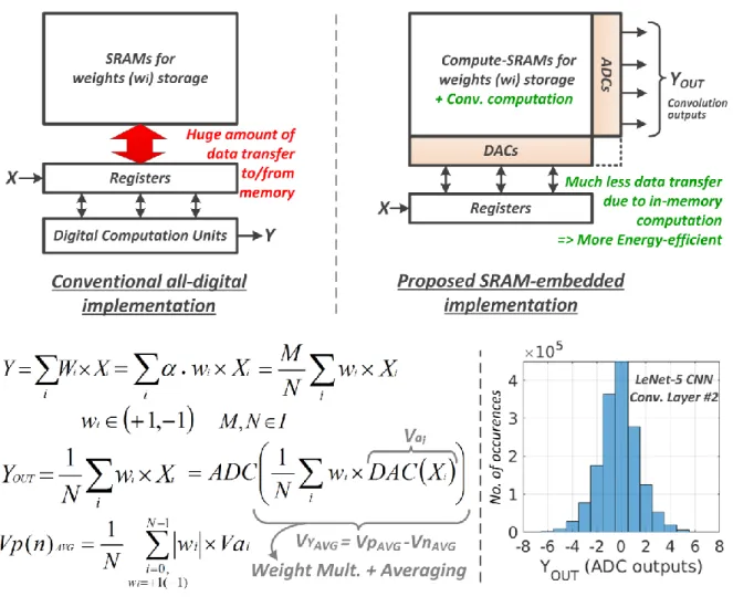
Convolutional Neural Networks (CNN) provide state-of-the-art results in a wide variety of machine learning (ML) applications, ranging from image classification to speech recognition. However, they are highly computation-intensive and require huge amounts of storage. Recent works have strived towards reducing the size of the CNNs, eg. [1] proposed a binary-weight-network (BWN), where the filter weights (wi’s) are +1/-1 (with a common scaling factor per filter: ‘α’). This leads to a significant reduction in the amount of storage required for the wi’s, making it possible to store them entirely on-chip. However, in a conventional all-digital implementation [2-3], reading the wi’s from the on-chip SRAMs leads to a lot of data movement per computation and hence, makes them energy-hungry. To reduce data-movement, and subsequently energy, we propose an SRAM-embedded convolution computation architecture (Fig. 1), which does not require reading the wi’s explicitly from the memory. To the best of our knowledge, this is the first work to demonstrate on silicon SRAM-based convolutions for CNNs. Prior works on embedded ML classifiers have focused on 1b outputs [4] or small number of output classes [5], both of which are not sufficient for CNNs. In this work we use 7b for inputs/outputs, which was found to be sufficient to maintain a good accuracy for most of the popular CNNs [1]. The convolution operation is implemented as voltage-averaging (Fig. 1), due to the wi’s being binary and the averaging factor (1/N) implementing the weight-coefficient ‘α’ (with a new scaling factor, M: implemented off-chip).
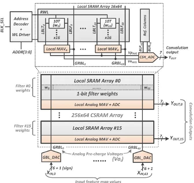
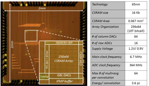
Fig. 2 shows the overall architecture of the 256x64 conv-SRAM (CSRAM) array. It is divided into 16 local arrays, each with 16 rows to reduce the area overhead of the ADCs and the local analog multiply-and-average (MAVa) circuits. Each local array is meant to store the binary weights, in the 10T bitcells (wi’s: ‘0’ for +1, ‘1’
its partial convolution outputs (YOUT). The input-feature-map values (XIN) are fed into column-wise DACs
(GBL_DAC), which pre-charge the global read bit-lines (GRBL) and the local bit-lines (LBL) to an analog voltage (Va) proportional to the digital XIN code. The GRBLs are shared by all the local arrays, implementing
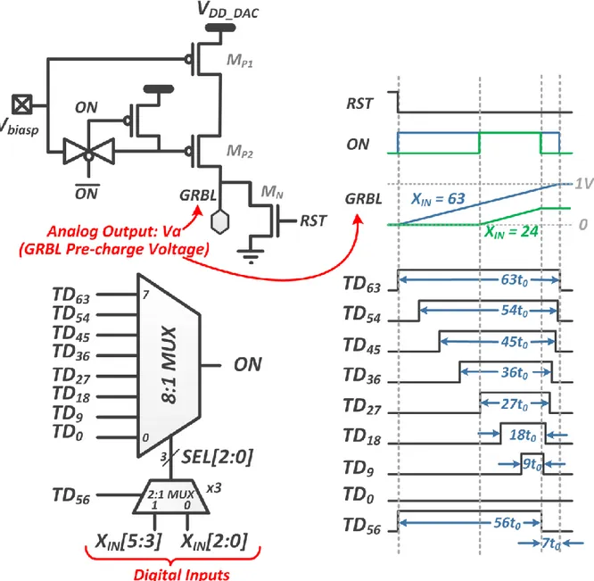
the fact that in CNNs each input is shared/processed in parallel by multiple filters. Fig. 3 shows the schematic of the proposed GBL_DAC circuit. It consists of a cascode PMOS stack biased in the saturation region to act as a constant current source. The GRBL is charged with this current for a time TON, directly proportional to
the XIN code. To have a better linearity of TON vs XIN, there should be only 1 ON pulse for every code to avoid
multiple charging phases. This is not possible to generate using signals with simple binary weighted pulse-widths. To address this issue, we propose an implementation in which the 3 MSBs of XIN are used to select
the ON pulse-width for the first half (TD56 = ‘1’) and the 3 LSBs for the second half (TD56 = ‘0’). An 8-to-1 mux
with 8 timing signals is shared during both the phases, to reduce the area overhead and the number of timing signals to route. In this way we could generate a single ON pulse for each XIN code, as shown for codes 63
and 24 in Fig. 3. This DAC architecture performs better than binary-weighted PMOS charging DACs [4] in terms of mismatch and linearity. This is because the same PMOS stack is used to charge the GRBL for all input codes. And the pulse-widths of the timing signals typically have less variations compared to those arising from PMOS VT mismatch.
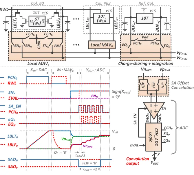
After the DAC pre-charge phase, the wi’s in a local array are locally evaluated by turning on a RWL, as shown
in Fig. 4. Next, the appropriate local bit-lines are shorted together horizontally to evaluate the average. This is implemented by the local MAVa circuit, which passes the voltages of the LBLT and LBLF to the positive
(VpAVG) and negative (VnAVG) voltage rails, depending on the sign of the input XIN (ENP is ON for XIN >0, ENN
is ON for XIN <0). The difference of VpAVG and VnAVG voltages is fed to a charge-sharing based ADC
(CSH_ADC) to get the digital value of the computation (YOUT). As seen from the histogram in Fig. 1, algorithm
Hence, a serial integrating ADC architecture is more apt in this scenario, compared to other area-intensive (e.g. SAR) and more power-hungry ones (e.g. flash). A PMOS-input sense-amplifier (SA) is used to compare VpAVG and VnAVG, and its output is fed to the ADC logic block. After the first comparison, which determines
the sign of YOUT, capacitive charge-sharing is used to integrate the lower of the 2 voltage rails with a reference
local column that replicates the local bit-line capacitance. This is continued until the voltage of the integrating rail exceeds the other one, at which point the SA output flips. This triggers the end of conversion and no further SA_EN pulses are generated for the SA. Fig. 4 shows the waveforms for a typical cycle of operation. To reduce the effect of the SA offset voltage on the YOUT value, a mux has been used at the input of the SA
to flip the inputs in alternate cycles.
The 256x64 CSRAM array was implemented in a 65nm LP CMOS process. Fig. 5 shows the measurement results for the GBL_DAC, which is used in the 5b mode by setting the LSB of XIN to ‘0’. To estimate the DAC
analog output voltage (Va), VGRBL for the 64 columns are compared to an external Vref voltage by column-wise
SA’s, used in the SRAM global read circuit. For each XIN, the Vref at which more than 50% of the SA outputs
flip is chosen as an average estimate of Va. An initial one-time calibration is needed to set Va = 1V for XIN =
31 (max. input code). As seen from Fig. 5, there is a good linearity in the DAC transfer function with DNL < 1LSB. Fig. 5 also shows the overall transfer function of the system consisting of the GBL_DAC, MAVa and
CSH_ADC circuits. For this experiment, all XIN’s are fed the same code, all wi’s are written the same value
and then the YOUT outputs are observed. The measurement results show good linearity in the overall transfer
function and low variation in the YOUT values, which is due to the fact that the variation in BL capacitance
(used for averaging and CSH_ADC) is much lower than transistor VT variation. The offset cancelation
technique further helps in reducing YOUT variation. It can be also seen from Fig. 5 that the energy/ADC scales
linearly with the output code, which is expected for the integrating ADC topology.
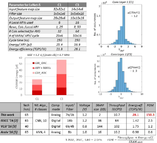
is used with the LeNet-5 CNN. 100 test images are run through the first two computation-intensive convolutional layers (C1, C3). We achieve a classification accuracy of 99%, which shows the robustness of the CSRAM architecture to compute convolutions. The distributions of YOUT in Fig. 6, show that both layers
has a mean ~1LSB, which justifies the use of the serial ADC topology. Fig. 6 also shows the overall energy of computation along with the different components. Layers C1 and C3 consume 4.23pJ and 3.56pJ per convolution, computing 25 and 50 MAV operations in each cycle respectively. Layer C3 achieves the best energy efficiency of 28.1 TOPS/W compared to 11.8 for layer C1, since C1 uses only 6 of the 16 local arrays. Compared to prior works, we achieve >16x improvement in energy-efficiency, and >60x higher FOM (Fig. 6) due to massively parallel in-memory analog computations. This demonstrates that the proposed SRAM-embedded architecture is capable of highly energy-efficient convolution computation that could enable low power ubiquitous ML applications for a smart Internet-of-Everything.
[Placeholder for Acknowledgements] References:
[1] M. Rastegari, et al., “XNOR-Net: ImageNet Classification Using Binary Convolutional Neural Networks”, arXiv:1603.05279, 2016.
[2] J. Sim, et al., “A 1.42TOPS/W Deep Convolutional Neural Network Recognition Processor for Intelligent IoE Systems”, ISSCC 2016, pp 264-265.
[3] B. Moons et al., “A 0.3–2.6 TOPS/W precision-scalable processor for real-time large-scale ConvNets”, VLSI Circuits 2016, pp. 1-2.
[4] J. Zhang, et al., “A machine-learning classifier implemented in a standard 6T SRAM array”, VLSI Circuits 2016, pp. 1-2.
[5] M. Kang, et al, “A 481pJ/decision 3.4M decision/s Multifunctional Deep In-memory Inference Processor using Standard 6T SRAM Array”, arXiv:1610.07501, 2016.
Fig. 1: Concept of embedded convolution computation as averaging in SRAMs for binary-weight convolutional neural networks.
Fig. 2: Overall architecture of the Conv-SRAM (CSRAM) showing local arrays, column-wise DACs and row-wise ADCs to implement convolution as weighted averaging.
Fig. 4: Architecture for the row-wise multiply-and-average, CSH_ADC circuits and operation waveforms for convolution computation.
Fig. 5: Measured performance of the GBL_DAC and CSH_ADC circuits in the CSRAM array and the effect of the offset cancelation technique.
Fig. 6: Measurement results (energy and output distribution) for the first 2 conv-layers of the LeNet-5 CNN for MNIST dataset; comparison with prior works.

![[PDF] Cours complet de programmation en Caml pour débutant | Cours informatique](data:image/gif;base64,R0lGODlhAQABAIAAAP///wAAACH5BAEAAAAALAAAAAABAAEAAAICRAEAOw==)