HAL Id: hal-03091723
https://hal.archives-ouvertes.fr/hal-03091723
Preprint submitted on 31 Dec 2020
HAL is a multi-disciplinary open access
archive for the deposit and dissemination of sci-entific research documents, whether they are pub-lished or not. The documents may come from teaching and research institutions in France or abroad, or from public or private research centers.
L’archive ouverte pluridisciplinaire HAL, est destinée au dépôt et à la diffusion de documents scientifiques de niveau recherche, publiés ou non, émanant des établissements d’enseignement et de recherche français ou étrangers, des laboratoires publics ou privés.
TSV-integrated Surface Electrode Ion Trap for Scalable
Quantum Information Processing
P. Zhao, J.-P. Likforman, H. Y. Li, J. Tao, T. Henner, Y. D. Lim, W. W. Seit,
C. S. Tan, Luca Guidoni
To cite this version:
P. Zhao, J.-P. Likforman, H. Y. Li, J. Tao, T. Henner, et al.. TSV-integrated Surface Electrode Ion Trap for Scalable Quantum Information Processing. 2020. �hal-03091723�
Page 1 of 4
TSV-integrated Surface Electrode Ion Trap for Scalable Quantum Information
Processing
P. Zhao1,3, J. P. Likforman2, H.Y. Li1, J. Tao3, T. Henner2, Y. D. Lim3, W. W. Seit1,C. S. Tan3,b), L. Guidoni2, a)
1Institute of Microelectronics, Agency for Science, Technology and Research (A*STAR), Singapore 117685 2Laboratoire Matériaux et Phénomènes Quantiques, CNRS - Université de Paris, F-75013 Paris, France 3School of Electrical and Electronic Engineering, Nanyang Technological University, Singapore 639798
In this study, we report the first Cu-filled through silicon via (TSV) integrated ion trap. TSVs are placed directly underneath electrodes as vertical interconnections between ion trap and a glass interposer, facilitating the arbitrary geometry design with increasing electrodes numbers and evolving complexity. The integration of TSVs reduces the form factor of ion trap by more than 80%, minimizing parasitic capacitance from 32 to 3 pF. A low RF dissipation is achieved in spite of the absence of ground screening layer. The entire fabrication process is on 12-inch wafer and compatible with established CMOS back end process. We demonstrate the basic functionality of the trap by loading and laser-cooling single 88Sr+ ions.
It is found that both heating rate (17 quanta/ms for an axial frequency of 300 kHz) and lifetime (~30 minutes) are comparable with traps of similar dimensions. This work pioneers the development of TSV-integrated ion traps, enriching the toolbox for scalable quantum computing.
Quantum information processing (QIP) platforms recently released from IonQ and Honeywell have highlighted the impressive development of surface electrode ion traps1,2. Taking advantage of
well-established microfabrication techniques (i.e., MEMS and CMOS), surface electrode ion traps exhibits flexible design, reproducible fabrication and mass production3.
More importantly, the possible integration with photonics components (i.e., waveguide, grating coupler 4-6 and photodetector7) enables precise control and
measurement on individual trapped ion. These features make surface electrode ion trap highly promising for large scale QIP. To scale close or even beyond noisy intermediate-scale quantum regime (NISQ, ~100 ions)8,
1D arrays, 2D arrays9,10 and quantum charge-coupled
device (QCCD) geometry11,12 have been proposed with
evolving electrodes layout complexity. However, this strategy opens significant challenges for electric signal delivery, since conventional bonding wires are not able to access the isolated island-like electrodes, and large number of wires will further impede laser beams.
The previous approach to mitigate this challenge is to employ multilayer metallization, where patterned metal layers and dielectric material are alternatively overlapped beneath surface electrode13-16. Small vias
through dielectric layers are required to build interconnections between different metal layers, while the metal layer in the bottom is often used as grounding plane to shield the silicon substrate from RF signal. The incorporation of routing leads underneath allows flexible design of surface electrodes geometry. However, this approach also comes with issues. First, as photonics layer is normally laid beneath following metallic layers due to its stringent wafer flatness requirement, the multilayer metallization above will significantly hamper its on-chip integration, and thus degrade the ion trap scalability. In addition, the thick dielectric layer (~10 μm) formation and patterning necessitate non-standard fabrication techniques, limiting the compatibility with large-scale
a) [email protected] b) [email protected]
foundry manufacturing17. Eventually, the multilayer
metallization may increase the coupling parasitic18,
resulting in high RF loss and heating of the device. Recently, the use of via as interconnection of ion trap has also been explored. As reported by N. D. Guise et al19,
polysilicon filled via with diameter of ~50 μm was used for signal delivery. However, due to the poor conductivity of polysilicon, only DC electrodes were contacted with vias and additional platinum silicide contacts were required as ohmic contacts between electrodes and polysilicon. In another work (H. Li et
al20), a ring trap was contacted with a 100 μm diameter
electrical via etched through a 70 μm glass substrate followed by 800 nm gold deposition. However, this customized process curtails the large-scale fabrication compatibility.
In order to overcome these limitations and further boost the scalability, the first Cu-filled TSV integrated ion trap is demonstrated in this work. With intrinsically small resistance, Cu-filled TSV are used as vertical connections between all the electrodes (including RF) and an interposer underneath. The first advantage of this approach, compared to multilayer metallization, is that the small footprint of TSV makes it highly compatible with photonics integration: the small diameter (20 μm) of TSV allows for compact and flexible electrode design. Besides, TSV eliminates the requirement for thick dielectric layer and the patterning of thin SiO2 layer (~3 μm) between electrode and substrate is of less complexity and foundry compatible. Additionally, as bonding wires are assigned to the interposer, the height difference between ion trap and interposer may mitigate laser beam blocking issues.
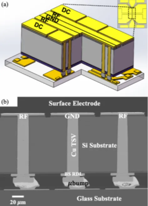
We designed the TSV integrated ion trap (TSV trap) starting from a previous 5 wire design21,22 that includes
bonding pads (WB, wire bonding trap). As shown in Fig. 1(a), TSV trap geometry only preserves the core region, eliminating the wire bonding pads and the connecting circuits present in the WB trap23. The original wire
Page 2 of 4 bonding pads are transferred to an interposer, reducing
drastically the surface of the electrodes. This minimizes undesired parasitic and mitigate the RF loss issue. The width and length of center three parallel electrodes (RF, GND and RF) are 80 and 2920 μm respectively, while the gap in between is 5 μm. TSV are designed with a diameter of 20 μm and depth of 100 μm. The pitch between TSVs is 100 μm. 10 TSVs are accommodated under RF electrodes, while 6 or 10 TSVs are accommodated under surrounding DC electrodes, depending on the electrode size. Micro bumps with a diameter of ~30 μm are located underneath every single TSV to support ion trap after assembling with interposer. The interposer is designed with a redistribution layer (RDL), acting as a bridge between the ceramic pin grid array package (CPGA) and the TSV trap for electrical signal transmission (Fig. 1(b)). The tested RDL geometry is a sort of extension of ion trap electrodes. Obviously, more complex routing can be implemented where necessary. While the TSV trap is made on a silicon substrate, we choose to use a glass substrate to fabricate the interposer, in order to minimize RF losses and simplify the fabrication process. To evaluate a possible effect of the electrode geometry modification between WB and TSV traps, a finite element modelling (FEM) is conducted. As expected, we find negligible effects on both the trapping height (~76 μm) and trapping depth (~80 meV with a RF amplitude VRF = 200V at 60 MHz).
Fabrication processes of both glass wafer (for interposer) and silicon wafer (for ion trap device) are compatible with standard back end process in CMOS foundry, in which 12-inch wafer are used and ~2,000 single dies with different design dimensions are fabricated simultaneously (Fig. 2(a) and (b)). For silicon wafer fabrication, blind vias are first etched through ~2.4 µm SiO2 and 100 µm Si before wafer frontside
patterning. To insulate Cu core from silicon, a TSV liner with thickness of 0.75 µm is uniformly deposited onto via sidewall. After Cu filling, two steps of chemical-mechanical polishing are required before and after annealing to completely remove Cu overburden. Next, the patterning of frontside SiO2 is conducted. Note that
SiO2 is designed with same geometry as electrodes, in
order to avoid undesired dielectric charging issue during ion trapping operation. To form electrodes, lithography defined electroplating of 3 µm Cu with 0.3 µm Au finish is employed. Following that, both wet etching and plasma etching are used to minimize the metal seed residue in the electrode gaps. After temporary bonding with handle wafer, the device wafer is thinned to ~100 µm by grinding and dry etching. Finally, three steps of lithography are conducted in sequence to define RDL, passivation layer and micro bumps on the wafer backside. On the other hand, the fabrication of glass interposer is similar with backside process of ion trap, where three steps of lithography are required, but the last one is to define under bump metallization (UBM) instead of micro bump. After wafer singulation, selected known good dies are bonded together. Eventually, bonded ion trap is assembled into CPGA, as shown in Fig. 2(c).
To assess the reliability of TSV liner, a voltage sweep from -200 to 200 V is applied to TSVs. It is found the maximum leakage current for a single TSV is about 7 × 10-12 A, suggesting 0.75 µm TSV liner is able to
withstand a voltage of 200 V and will not breakdown. Also, a resistance measurement is performed between RF and GND electrodes on both ion trap and glass interposer. The results shows a minimum resistance of ~2 × 10⁸ Ω , which is sufficiently large for voltage
insulation. In addition, the connection between interposer RDL and corresponding surface electrodes is checked. No open circuit is found, indicating a firm and stable signal transmission path.
One of the major challenges for ion trap with semiconductor substrate is the high RF dissipation24-26.
To evaluate the RF performance of TSV trap, a WB trap with silicon substrate but no grounding plane is used for comparison. Given that the power loss is proportional to the square of parasitic capacitance of ion trap21,25,a
capacitance-voltage (C-V) test is first performed to measure the capacitance between RF and GND electrodes. The result shows that TSV trap has a capacitance of 3 pF, as compared to 32 pF of WB trap. This 90% capacitance decrease can be attributed to the
FIG. 1. (a) 3D schematic of TSV-integrated ion trap (TSV trap, not to scale). The geometry is modified from wire bonding (WB) trap (inset). (b) Cross-sectional SEM image of TSV trap. The surface electrode and interposer RDL are interconnected by TSV and micro bumps.
FIG. 2. (a) Fabricated TSV die on 12-inch silicon wafer. (b) Fabricated interposer on 12-inch glass wafer. (c) Packaged TSV trap in a CPGA.
Page 3 of 4 significant reduction of electrode surfaces (from 4.5 to
0.2 mm2, for single RF electrode). A resonance test is
then conducted27. As shown in Fig. 3(a), TSV trap
features a two orders of magnitude RF loss reduction as compared to WB trap. Its resonance peak is close to that of a standard RF capacitor, which suggests that a low RF loss is achieved for TSV trap even though no grounding plane is added.
On-chip S parameter measurement is carried out and the overlapping curves from TSV die (without interposer) and TSV trap (with interposer) in Fig. 3(b) indicate that negligible loss is induced by the incorporation of glass interposer.
The packaged TSV trap of Fig. 3(c) is tested in a laser-cooled trapped ion setup by loading it with single
88Sr+ ions. Technical details of the setup are described
elsewhere28,29.
We insert the CPGA in the vacuum cell and then bakeat 150°Cforone week. The resulting base pressure is approximately 4 × 10-11 mbar, demonstrating the
excellent ultra-high vacuum compatibility of the packaged ensemble (trap, interposer and micro-bumps). We drive the two RF lines with an impedance-matching toroidal resonant transformer at a frequency WRF/2p = 30
MHz. We only test the trap with amplitudes VRF below
120 V. For VRF larger than 85 V we notice a slight
increase of the base pressure (of the order of some 10-11
mbar), probably associated to residual heat dissipation in the trap. We load the trap by two-colour photo-ionizing a thermally sublimated Sr atomic beam30,31.
The 88Sr+ ions are Doppler-cooled addressing the
52S1/2 → 52P1/2 transition (711 THz, 422 nm). To avoid
optical pumping into the metastable 42D3/2 state we use
two additional lasers (“repumpers”) addressing the 299~THz 42D
3/2 → 52P3/2 transition and the 290 THz
42D5/2 → 52P3/2 transition (incoherent repumping
scheme32). 711 THz photons scattered by the ion are
collected by a home-made objective with numerical aperture of 0.4 and detected by a photomultiplier in photon-counting mode. An overall collection efficiency of (1.8±0.2 × 10⁻³) is measured using sequential
acquisitions that require the 275 THz “readout” laser addressing the 42D3/2 → 52P1/2 transition33.
We also acquire images of the trapped and cooled
ions with an electron-multiplier CCD camera (Andor Luca), as shown in Fig. 4(a).
Excess of micromotion in the trap is minimized using a single photon time correlation method34. The
compensation DC voltages are found to be stable in a week basis. The lifetime of a laser-cooled ion in the trap is of the order of 30 minutes, compatible with the vacuum level.
We evaluate the trap performances by measuring the heating rate with the technique of Doppler re-cooling35.
To this purpose we operate the trap with an axial frequency wz/2p = 300 kHz and radial frequencies
around wr/2p = 2.6 MHz. A sequential acquisition first
cools the ion during 500 ms, then switches off the cooling laser for a waiting (heating) time th, and then switches on
again the cooling laser triggering the acquisition of single photons timestamped with arrival times. The two-level-atom approximation needed for the analysis of the acquired data 36 is well fulfilled by the incoherent
repumping approach: we show in Fig. 4(b, inset) a single-ion fluorescence spectrum that displays a Lorentzian line-shape. We record single shot and average histograms of the scattered photons as a function of the emission time for different heating times th. An example
of averaged histogram is plotted in Fig. 4(b) with the corresponding fit obtained with the hypothesis of a Maxwell-Boltzmann velocity distribution (T=5.1 K for th
= 20 s). From the analysis of all the experimental sets the heating rate of the trap is evaluated at 250±15 mK/s that corresponds to 17 axial quanta per millisecond. The calculated figure of merit corresponding to the noise spectral density times the motional frequency37 is
wz*SE(wz) =1.5 ×10⁻⁴ (V/m)2. While it does not set a new
record, this result favorably compares to non-decontaminated non-cryogenics traps of similar dimensions38.
In conclusion we demonstrate the successful fabrication in a CMOS foundry and the full functionality of a silicon surface ion trap in which all the electric connections (i.e., DC and RF) are realized with through silicon vias. We load single 88Sr+ ions into the trap and
we find that the heating rate, lifetime and stability are
FIG. 3. (a) Resonance test of ion traps packaged into CPGA. The reference curve is from a standard capacitor. (b) On-chip S parameter test of TSV die before and after bonding with glass interposer.The curves from WB trap are also plotted for comparison, showing TSV trap can reduce the insertion loss from -2.2 to -0.1 dB (at 50 MHz). The inset shows a three-pin probe contacting on electrodes surface.
FIG. 4. (a) Image of a single 88Sr+ laser-cooled ion trapped above the
surface of the TSV trap; the image field covers a 1 mm2 area, the trap
is illuminated by a light emitting diode. (b) Counting rate as a function of the re-cooling time averaged over 120 realisations for a heating time th = 20 seconds (blue squares). The continuous black curve is the best
one-parameter fit that allows us to retrieve a temperature increase T=5.1 K. Inset: fluorescence spectrum of the ion as a function of the detuning of a probe beam that scans the cooling transition (red circles); the continuous black curve is a Lorentzian fit that shows that the incoherent repumping scheme leads to a very good two-level atom approximation.
Page 4 of 4 comparable with other traps of similar dimensions. This
work pioneers the development of TSV-integrated ion traps, enriching the toolbox for trapped ion based scalable quantum computing. In particular the TSV approach is compatible with photonic circuit integration4-6, insertion of a ground screening layer to
eliminate trap-heating, and in the future could be extended to glass substrates29.
We would like to thank technical staffs in in Institute of Microelectronics, A*STAR for their technical supports on trap fabrication and packaging. We acknowledge the funding support from A*STAR Quantum Technology for Engineering (A1685b0005). The data that support the findings of this study are available from the corresponding author upon reasonable request.
1K. Wright, K. Beck, S. Debnath, J. Amini, Y. Nam, N. Grzesiak, J.-S.
Chen, N. Pisenti, M. Chmielewski, and C. Collins, Nature communications 10, 1 (2019).
2J. Pino, J. Dreiling, C. Figgatt, J. Gaebler, S. Moses, C. Baldwin, M.
Foss-Feig, D. Hayes, K. Mayer, and C. Ryan-Anderson, arXiv preprint arXiv:2003.01293 (2020).
3C. D. Bruzewicz, J. Chiaverini, R. McConnell, and J. M. Sage,
Applied Physics Reviews 6, 021314 (2019).
4K. K. Mehta, C. D. Bruzewicz, R. McConnell, R. J. Ram, J. M. Sage,
and J. Chiaverini, Nature nanotechnology 11, 1066 (2016).
5R. J. Niffenegger, J. Stuart, C. Sorace-Agaskar, D. Kharas, S.
Bramhavar, C. D. Bruzewicz, W. Loh, R. McConnell, D. Reens, and G. N. West, arXiv preprint arXiv:2001.05052 (2020).
6K. K. Mehta, C. Zhang, M. Malinowski, T.-L. Nguyen, M. Stadler, and
J. P. Home, Nature 586, 533 (2020).
7S. Todaro, V. Verma, K. McCormick, D. Allcock, R. Mirin, D.
Wineland, S. Nam, A. Wilson, D. Leibfried, and D. Slichter, arXiv preprint arXiv:2008.00065 (2020).
8J. Preskill, Quantum 2, 79 (2018).
9P. C. Holz, S. Auchter, G. Stocker, M. Valentini, K. Lakhmanskiy, C.
Rössler, P. Stampfer, S. Sgouridis, E. Aschauer, and Y. Colombe, Advanced Quantum Technologies, 2000031 (2020).
10U. Tanaka, K. Suzuki, Y. Ibaraki, and S. Urabe, Journal of Physics
B: Atomic, Molecular and Optical Physics 47, 035301 (2014).
11D. Kielpinski, C. Monroe, and D. J. Wineland, Nature 417, 709
(2002).
12K. R. Brown, J. Kim, and C. Monroe, npj Quantum Information 2, 1
(2016).
13J. M. Amini, H. Uys, J. H. Wesenberg, S. Seidelin, J. Britton, J. J.
Bollinger, D. Leibfried, C. Ospelkaus, A. VanDevender, and D. J. Wineland, New J. Phys. 12, 033031 (2010).
14P. L. W. Maunz, Technical Report of Sandia (2016),
https://prod-ng.sandia.gov/techlib-noauth/access-control.cgi/2016/160796r.pdf
15B. Tabakov, F. Benito, M. Blain, C. R. Clark, S. Clark, R. A. Haltli,
P. Maunz, J. D. Sterk, C. Tigges, and D. Stick, Physical Review Applied 4, 031001 (2015).
16A. Bautista-Salvador, G. Zarantonello, H. Hahn, A.
Preciado-Grijalva, J. Morgner, M. Wahnschaffe, and C. Ospelkaus, New J. Phys.
21, 043011 (2019).
17Z. D. Romaszko, S. Hong, M. Siegele, R. K. Puddy, F. R.
Lebrun-Gallagher, S. Weidt, and W. K. Hensinger, Nature Reviews Physics, 1 (2020).
18P. C. Holz, S. Auchter, G. Stocker, M. Valentini, K. Lakhmanskiy, C.
Rössler, P. Stampfer, S. Sgouridis, E. Aschauer, and Y. Colombe, arXiv preprint arXiv:2003.08085 (2020).
19N. D. Guise, S. D. Fallek, K. E. Stevens, K. Brown, C. Volin, A. W.
Harter, J. M. Amini, R. E. Higashi, S. T. Lu, and H. M. Chanhvongsak, J. Appl. Phys. 117, 174901 (2015).
20H.-K. Li, E. Urban, C. Noel, A. Chuang, Y. Xia, A. Ransford, B.
Hemmerling, Y. Wang, T. Li, and H. Häffner, Phys. Rev. Lett. 118, 053001 (2017).
21J. Chiaverini, R. B. Blakestad, J. Britton, J. D. Jost, C. Langer, D.
Leibfried, R. Ozeri, and D. J. Wineland, arXiv preprint quant-ph/0501147 (2005).
22S. Seidelin, J. Chiaverini, R. Reichle, J. J. Bollinger, D. Leibfried, J.
Britton, J. Wesenberg, R. Blakestad, R. Epstein, and D. Hume, Phys. Rev. Lett. 96, 253003 (2006).
23P. Zhao, J. Tao, H. Y. Li, Y. D. Lim, L. Guidoni, and C. S. Tan,
presented at the 2019 IEEE 21st Electronics Packaging Technology Conference (EPTC), 2019.
24R. C. Sterling, University of Sussex, 2012.
25M. Niedermayr, K. Lakhmanskiy, M. Kumph, S. Partel, J. Edlinger,
M. Brownnutt, and R. Blatt, New J. Phys. 16, 113068 (2014).
26K. R. Brown, J. Chiaverini, J. Sage, and H. Häffner, arXiv preprint
arXiv:2009.00568 (2020).
27J. Tao, H. Y. Li, Y. D. Lim, P. Zhao, A. A. A. Apriyana, L. Guidoni,
and C. S. Tan, IEEE Transactions on Components, Packaging and Manufacturing Technology (2019).
28B. Szymanski, R. Dubessy, B. Dubost, S. Guibal, J.-P. Likforman,
and L. Guidoni, Appl. Phys. Lett. 100, 171110 (2012).
29J. Tao, J. Likforman, P. Zhao, H. Li, T. Henner, Y. Lim, W. Seit, L.
Guidoni, and C. Tan, arXiv preprint arXiv:2002.11470 (2020).
30K. Vant, J. Chiaverini, W. Lybarger, and D. Berkeland, arXiv
preprint quant-ph/0607055 (2006).
31M. Brownnutt, V. Letchumanan, G. Wilpers, R. Thompson, P. Gill,
and A. Sinclair, Applied Physics B 87, 411 (2007).
32D. Allcock, J. Sherman, D. Stacey, A. Burrell, M. Curtis, G. Imreh,
N. Linke, D. Szwer, S. Webster, and A. Steane, New J. Phys. 12, 053026 (2010).
33M. Ramm, T. Pruttivarasin, M. Kokish, I. Talukdar, and H. Häffner,
Phys. Rev. Lett. 111, 023004 (2013).
34D. Berkeland, J. Miller, J. C. Bergquist, W. M. Itano, and D. J.
Wineland, J. Appl. Phys. 83, 5025 (1998).
35R. J. Epstein, S. Seidelin, D. Leibfried, J. H. Wesenberg, J. J.
Bollinger, J. M. Amini, R. B. Blakestad, J. Britton, J. P. Home, W. M. Itano, J. D. Jost, E. Knill, C. Langer, R. Ozeri, N. Shiga, and D. J. Wineland, Phys. Rev. A 76, 033411 (2007).
36R. Epstein, S. Seidelin, D. Leibfried, J. Wesenberg, J. J. Bollinger, J.
Amini, R. Blakestad, J. Britton, J. Home, and W. M. Itano, Phys. Rev. A 76, 033411 (2007).
37M. Brownnutt, M. Kumph, P. Rabl, and R. Blatt, Rev. Mod. Phys. 87, 1419 (2015).
38I. A. Boldin, A. Kraft, and C. Wunderlich, Phys. Rev. Lett. 120,