Chemical and Biomedical Sensors Using
Two Dimensional Materials
by Mantian Xue
B.S. Material Science and Engineering University of Illinois at Urbana-Champaign, 2017
Submitted to the Department of Electrical Engineering and Computer Science in partial fulfillment of the requirements for the degree of
Master of Science in Electrical Engineering and Computer Science at the
MASSACHUSETTS INSTITUTE OF TECHNOLOGY
September 2019
©Massachusetts
Institute of Technology 2019. All rights reservedSignature of Author:
Signature redacted
Department of Electrical Engineering and Computer Science
Signature redacted
August 30, 2019Certified by: ...
Tomis Palacios Professor of Electrical Engineering and Computer Science
1) Thesis Supervisor
Certified by:
...
Signatureredacted....
MASSACHUSETTS INSTITUTE /
of rECHNOLOGY > Leslie A. Kolodziejski
F;-OC0301
Professor of Electrical Engineering and Computer ScienceOCT 0 32019
Chair, Department Committee on Graduate Students
LIBRARIES"
Two Dimensional Materials Based Sensors for Chemical and Biological
Applications
by Mantian Xue
Submitted to the Department of Electrical Engineering and Computer Science on August 30, 2019, in Partial Fulfillment of the
Requirements for the Degree of
Masters of Science in Electrical Engineering and Computer Science
Abstract
We are at the onset of a revolution in chemical and medical sensors. Traditional sen-sors are bulky and difficult to use. Many researchers have started to build easy-to-use in-home healthcare monitoring system such as wearable sweat sensors. In order to make such system practical, sensors need to combine high sensitivity, high selectivity, fast re-sponse time and small signal drift. The sensors also need to cover a wide range of rec-ognizable chemicals and molecules. Two-dimensional materials are perfect candidate as next-generation sensing materials because of their unique electrical, optical, mechanical and chemical properties. In this thesis, the fabrication and device technology of state-of-the-art graphene-based chemical sensor was discussed. A new 2D materials patterning technology and various passivation approaches were also studied. By using these novel technologies, three types of sensing devices that aims to push the development of bet-ter healthcare monitoring system were developed. A graphene-based biosensor for ligand detection was made with high sensitivity and a wide span of detection range. Graphene sensor arrays coupled with various types of ion-selective membranes were also developed. High sensitivity, selectivity and reversibility were achieve for detection of ionized calcium, sodium and potassium in electrolyte. FinallyMoS2 were explored to amplify the signal
and achieve high sensitivity at low concentration as well as an easier measurement scheme. All three sensors will serve as building blocks for the realization of next-generation chem-ical and biomedchem-ical sensor systems.
Thesis Supervisor: Tomas Palacios Title: Professor of Electrical Engineering
Contents
1 Introduction
1.1 Project Motivation . . . .
1.2 Introduction to Two Dimensional Materials 1.2.1 Introduction to Graphene . . . . . 1.2.2 Introduction toMoS2 . . . . . . . . 1.3 Thesis Outline . . . . 2 Device Technology 2.1 Cleanness of film . . . . 2.2 Passivation . . . . 2.3 Conclusion . . . . 3 Graphene-based Biosensors
3.1 Electrolyte-gated graphene field-effect 3.2 pH sensing . . . . 3.3 Ligand Detection with GPCR . . . . 3.3.1 Device Structure . . . . 3.3.2 Sensor Response . . . . 3.4 Conclusion . . . . transistors 11 11 . . . . . 12 . 1 13 . . . . . 16 . . . . . 19 21 21 25 34 36 36 37 40 42 43 46 47 47 50 53 56 58 4 Graphene-based Ion Sensing
4.1 Theory of Ion Selective Membrane . . . . 4.2 Sensor Array Structure and Performance 4.3 Ca2+ ion sensor . . . . 4.4 Na+ ion sensor . . . . 4.5 K+ ion sensor . . . .
4.6 Integration of multiple ion sensor . . . . 60
4.7 C onclusion . . . . 62
5 MoS2-based Sensors 64 5.1 Device Structure . . . . 64
5.2 pH Sensing Mechanism . . . . 65
5.3 Sensor Performance . . . . 68
5.4 C onclusion . . . . 69
6 Conclusion and Future Work 70
Bibliography 72
Appendices 83
A Standard Photolithography Recipes 83
B Recipe for graphene-based pH sensor 85
C Recipe for graphene-based ligand sensor 87
D Recipe for graphene-based sensor array 90
List of Figures
1.1 The family of 2D materials. Figure adopted from [1] . . . . 13 1.2 (a)The carbon atomic a and 7r orbitals in the sp2
honeycomb lattice [14] (b) Electronic dispersion in the honeycomb lattice. Left: energy spectrum. Right: zoom in of the energy bands close to one of the Dirac points [13]. (c)Ambipolar electric field effect in single-layer graphene. The insets show its conical low-energy spectrum [2] . . . . 15 1.3 (A) Atomic structure for single layer transition metal dichalcogenides (TMDs)
in the 2H, 1T, and IT' phases, (B) periodic table of elements involved lay-ered TMDs, (C) evolution of the band structure for 2H-MoS2 with
decreas-ing number of layers, and (D) the schematic representation of the band structure for 2H-MoS2. This TMD overview image is reproduced from
M anzeli et al. [46] . . . . 17 2.1 Schematics for PMGI/SPR700 bilayer Patterning Process. Green film
rep-resents PMGI and orange film reprep-resents SPR700 . . . . 23 2.2 AFM Images of graphene films on SiO2 substrate with different photoresist
treatm ents . . . . 24 2.3 Effect of NMP Treatment with PMMA Processed Graphene film onSiO2
substrate. (a) PMMA processed graphene, (b) PMMA processed graphene after NMP overnight,(c)microscrope image of patterned graphene film after NM P treatm ent . . . . 25 2.4 AFM images of ALD dielectric on (a)graphene and (b) MoS2. Figures
adopted from [76] and [78] . . . . 26 2.5 AFM images of ALD A1203 on (a)graphene and (b)MoS2 surface with Al
2.6 (a)Hysteresis of electrolyte-gated graphene FETs without A1203
passiva-tion (b)hysteresis of electrolyte-gated graphene FETs with A1203 passivation 29
2.7 Effect of A1203 passivation on electrolyte-gated graphene FETs' I-V
char-acteristic . . . . 30 2.8 Sensor response and structure of device (a) SU-8 passivation and (b) with
oxide passivation . . . . 32 2.9 I-V Characteristics of MoS2 Back-gated Transistors.(a) Output
charac-teristics without oxide, (b)output characcharac-teristics with oixde, (c) transfer characteristics without oxide, (d) transfer characterstics with oxide . . . . 33 2.10 Transfer characteristics of MoS2 based transistors with different types of
passivation. Figure adopted from Yu et al. [78]. . . . . 34
3.1 (a)Device structure and measurement setup for electrolyte-gated graphene field-effect transistors. (b)Three most common models to describe electric double layers, figure taken from [36] . . . . 37 3.2 Change in Dirac point with respect to pH value . . . . 39 3.3 Schematics of 2D lattice of GPCR/S-layer complex. Images taken from
R ui Q ing, PhD . . . . 41 3.4 AFM images to show surface morphology of S-layer and GPCR/S-layer
complex on silicon substrate. Images taken from Rui Qing,PhD. . . . . 41 3.5 (a)Mask file of the graphene-based ligand sensor with GPCR (b)
Measure-ment setup and fluid chamber . . . . 42 3.6 I-V response and schematics upon exposure of CXCL12 ligands with (a)
bare graphene, (b) S-layer and (c) GPCR/S-layer complex. Ids is normal-ized to its minimum value. Black stars represent ligand, green lines rep-resent S-layer, orange circles with black stars reprep-resent ligand bind with
G PCR protein. . . . . 44 3.7 Sensor response with respect to ligand concentration demonstrates good
linear relation between C/S and C (R2 = 0.992). S is defined as relative change in Dirac point. . . . . 46
4.1 (a) Graphene Ca2+ sensor diagram depicting measurement setup and equi-librium charge distribution. R- represents lipophilic anionic site. (b) schematic diagram showing the electrostatic potential as a function of dis-tance from graphene surface. The dash line indicates the potential distri-bution when zero Ca2+ concentration gradient is present between ISM and electrolyte. (c) idealized graphene Ca2+ sensor I-V characteristic response. 48
4.2 Mask desgin for graphene-based sensor array. Top-right is a zoom-in picture of the sensing area. Insert shows the mask of an individual graphene sensor. Bottom-right is a microscope image of a graphene sensor on the array chip after fabrication . . . . 51
4.3 (a) I-V characteristics of 244 working electrolyte-gated graphene transis-tors on one chip with Vd, = 300 mV.1uM NaCl solution was used as the electrolyte. (b)distribution of the Dirac points . . . . 52
4.4 ((a) Shift if I-V characteristic of a calcium sensor under different concen-tration, (b)slope of the average Dirac point as a function of ionized calcium concentration, error bar indicates the standard deviation. The sample size is 196 and all measurements are taken at Vd, = 300 mV. . . . . 54
4.5 Ca2+ sensor behaviors at different period of time. All measurements were taken using the same chip under same bias V,, = - 0.4 to 0.9V, Vd, = 300 m V . . . 55
4.6 Shift of average Dirac point as a function of ionized sodium concentration, error bar indicates the standard deviation. The sample size is 213 and all measurements are taken at Vd, = 300 mV. . . . . 56
4.7 Graphene Na+ sensor conductance transient response to changing concen-trations in ionized sodium. The sample size is 213 and the bias conditions are VdS=300 mV, VGS=-0.l V. Data is normalized with respect to the response at 1 mM of each sensor. . . . . 57
4.8 (a)Mean sensitivity response showing excellent sensitivity and reversibility over several orders of magnitude change in ionized sodium concentration. The percentage change in conductance is normalized with respect to the data taken at 1 mM and the error bars are given by the standard deviation. (b) Histogram shows reproducibility distribution of 213 individual devices. X-axis is the percentage difference between the fitted slope of increasing sodium concentration and that of decreasing sodium concentration. . . . . 58 4.9 Graphene K+ sensor response with change in potassium ion concentration.
The sample size is 193 and the bias conditions are Va=300 mV . . . . 59 4.10 (a)The non-linearity in change in conductance with different potassium
concentration for K+ sensor array. (b)I- V characteristics for the K+ sensors under 1 M KCl solution. The black dash-line indicates the slice of Id, at V gs = 0V . . . . 60 4.11 Sensor response with change in sodium concentration. Black line is for
sensors with calcium ISM and red line is for sensors with sodium ISM. The difference in slope indicates good selectivity . . . . 61 4.12 (a) Printed ISM on graphene sensor array chip. (b) Proposed chip design
for multiplexed sensor array. . . . . 62 5.1 Device structure and pH sensing mechanism forMoS2-based pH sensor . . 65
5.2 MoS2 Transfer characterstic . . . . 66
List of Tables
2.1 Surface roughness of graphene film after different treatment . . . . 24 4.1 Performance comparison of Ca2+ sensors based ion-selective membranes . . 54 4.2 Stability of Ca2+ sensor . . . . 55 4.3 Summary of Ion Sensors Performance . . . . 60
Chapter 1
Introduction
1.1
Project Motivation
Traditionally, the information regarding ones health would need to be gathered in test centers through either non-invasive or invasive tests such as X-ray and blood analysis. However, running such tests are expensive and time-consuming. Recently there has been significant work to develop more cost-efficient and easy-to-use health monitoring systems to replace or complement the traditional tests. These systems normally consist of a set of chemical and biological sensors, connected to a data acquisition and data processing element. With such system, ones can collect crucial information regarding their health in real time. This is important because the trend in healthcare is shifting toward active disease prevention instead of passive [29, 45]. There is a great interest on recognition of body vital signs and biomarker for such early disease diagnosis. This includes prevention of disease before it occurs and controlling progression of disease that already happened [35, 21]. By having an in-home healthcare monitor system with sensors dedicated to specific biomarkers, measurements can be taken more frequently thus providing better chance for early diagnosis.
In addition, personalization of medical information can also be important for effective early diagnosis. Each individual has a unique profile regarding health status [29]. With the data collected by in-home monitoring system, a specific baseline could be generated for each individual in terms of human physiological values and important biomarkers.
Through continuous monitoring it is thus easier to detect abnormal signals and improve the efficiency and accuracy of early diagnosis [29, 45]. It would also help to better identity treatment needs and provide data on the body's response to a treatment thus helping to evaluate the effectiveness of the treatment, leading to improvement of ones well-being.
An important aspect of building a practical in-home easy-to-use healthcare monitoring system is to have high-performance chemical and biological sensors. These sensors need to have high accuracy, high selectivity, fast response time and high stability over time. Two-dimensional (2D) materials are particularly promising candidates for chemical and biological sensing applications due to their high surface-to-volume ratio. This allows a large portion of their bulk material properties to be modulated in response to chemical changes occurring at or near the surface, generally leading to enhanced sensitivity. The mechanical flexibility of 2D materials is another advantage for applications like flexible and wearable electronics. Some 2D materials also have unique optical and mechanical properties that can be used for optical or strain sensors.
This Master's thesis aims to develop next-generation chemical and biological sensors by utilizing the unique properties of 2D materials. In this project, a novel ligand sensor is developed using graphene as the signal transducer. To reduce device variation and achieve higher accuracy, a sensor array is also developed using graphene and ion-selective membranes to monitor the balance of important electrolyte in body fluid. Furthermore, MoS2 is explored as an alternative sensing material to achieve easier measurement schemes
and better amplified the electrical signal. By demonstrating highly sensitive, selective and accurate sensors, this project takes one step further in the process of developing the next-generation health monitoring system.
1.2
Introduction to Two Dimensional Materials
This section introduces select 2D materials that exhibit high potential in chemical and bio-sensing application. Shown in Figure 1.1 is a summary of the 2D materials family categorized according to their electrical properties. For sensing application, the detection of analytes is achieved by monitoring the electrical signal change in the channel material.
2D insulators such as h-BN are not appropriate for such application. Graphene and MoS2 are the representative materials for 2D semi-metals and 2D semiconductors, which will be focused in section below.
Insulator
h-BN or
-0000-'i
BP family Graphenefamily
HI-VJ family TMD(MX,)family
2',,WSe,SflS,42 ,S=
Figure 1.1: The family of 2D materials. Figure adopted from [1]
1.2.1
Introduction to Graphene
Graphene, a single layer of graphite, is the most studied and mature semi-metal material in the 2D family. The first successful isolation of graphene film was obtained in An-dre Geim's group in 2004 by mechanical exfoliation of highly oriented pyrolitic graphite (HOPG) [49]. Graphene consists of a 2D plane of carbon atoms arranged in a hexag-onal lattice. The carbon atoms are connected with one ir-bond and three a-bond via
sp2 hybridization. The in-plane a-bonds provide mechanical strength in graphene and their electrons are localized. The ir-bonds are delocalized and the charge transport within in ir-bonds largely determines the electrical property of graphene. The ir-bonds can be influenced by environmental changes and the electrical proprieties in graphene will then be altered. In this way, chemical signals can be transformed into electrical signals in graphene. Many researches have demonstrated graphene's innate sensitivity towards a variety of gas molecules [58, 62, 26].
Graphene's excellent electrical properties find their origin in its pronounced ambipolar electric field effect. Charge carriers can be tuned between electrons and holes continuously with the carrier concentration as high as 1013 cm-2 under ambient conditions [50, 51, 2]. The mobility of graphene at room temperature can exceed 15,000 cm2
/Vs [2]. Moreover, research has shown that the mobility of graphene shows weak dependence on temperature. This means mobility is still limited by impurity scattering at room temperature, and by increasing the distance to these impurities the mobility can be increased up to 100,000 cm2
/Vs [2]. The ballistic transport on sub-micron scale in graphene makes the mobility remains high even at high carrier concentration (>1012
cm-2
) in doped graphene [2]. Even though graphene mobility in practical layers are typically reported in the range of 500
- 10,000 cm2
/Vs, it is still better than that most conventional materials such as silicon. High mobility in graphene makes it more responsive to environmental changes and thus increase the sensor sensitivity. It also provides better frequency response and higher signal-to-noise ratio in chemical sensors [15, 62, 56].
Graphene also has a unique band structure and charge carriers. Different from tra-ditional materials whose electronic properties can be described through the Schrodinger equation, the charge transport in graphene is better described by the relativistic Dirac equation [2]. Shown in Figure 1.2 (b) is the low-energy band structure of graphene. The conical-shape of the band structure makes graphene a zero-band gap or semi-metal mate-rial. The charge neutrality point, where the conduction band and valence band meets, is referred as the Dirac point (DP). The Dirac equation is a direct consequence of graphene's unique crystal lattice. The periodic potential of the honeycomb lattice gives rise to quasi-particles, called massless Dirac fermions, at low energy state. These quasiparticles have an effective speed of VF - 106m/s, which is roughly 1/300 of speed of light [2]. The large
value of VF allow the charge carries in graphene to move at a high speed, which can be advantageous for high sensitive and fast response time.
In additional to its electrical properties, the mechanical capabilities of graphene also make this material a strong candidate in next-generation sensing. The Young's modulus for graphene can be close to 1 TPa [70]. The high mechanical strength and high flexibility
#
6 1K t 46 4 2; (a) (b) (c)Figure 1.2: (a)The carbon atomic a and ir orbitals in the sp2 honeycomb lattice [14] (b) Electronic dispersion in the honeycomb lattice. Left: energy spectrum. Right: zoom in of the energy bands close to one of the Dirac points [13]. (c)Ambipolar electric field effect in single-layer graphene. The insets show its conical low-energy spectrum [2]
of graphene make it ideal for flexible and wearable electronics. It is also promising for biomedical implants since it is able to accommodate on the surrounding biological tissue without experiencing stress or fatigue [58]. In addition, graphene's sp2 carbon surface allow strong but non-destructive interactions at cellular level [58]. The high chemical stability of graphene, also makes it intrinsically biocompatible, which is very important for biomedical devices.
A critical step in developing high-performance graphene-based sensor device is to be able to synthesize graphene films with high quality and repeatability. Mechanical exfoliation from Highly oriented pyrolytic graphite (HOPG) has been the simplest method to obtain graphene since 2004 [49]. This method is easy and low-cost thus is perfect for quick demonstration of ideas. However, graphene flakes obtained form mechanical exfoliation usually have irregular shapes and orientation. The size of flakes is typically limited to a few microns. Another approach to synthesize graphene is to anneal hexagonal SiC crystal. At high temperature, the top layers of SiC crystal decompose in to Si and C atoms. The Si atoms desorb and the carbon atoms remaining on the surface rearrange and re-bond to form epitaxial graphene layers [5, 7]. Graphene formation on SiC has fast kinetics, which makes it difficult to control the growth thickness. The resulting film is usually multilayered and not uniform across the wafer [5]. Chemical vapor deposition (CVD) is the most commonly used technique to synthesis high-quality, large-area graphene films. In general, CVD process involves activation of carbon-containing precursors to
desired vaporous phase, transport of reacting gaseous species and heterogeneous surface reaction on the substrate [65]. Depending on the growth substrate and growth condition, carbon atoms can directly form a graphene layer on the surface of the substrate or dissolve inside the substrate and then precipitate to the surface forming a graphite film [65]. CVD graphene exhibits outstanding electrical and mechanical proprieties similar to the exfoliated graphene flakes [5]. Large-area, high quality CVD graphene grown on copper film is the most commonly used for graphene-based devices in literature. Graphene film can be transferred onto various substrates by standard wet transfer techniques [68, 65].
1.2.2
Introduction to MoS
2The second category of materials are 2D semiconductors, and more specifically transition metal dichalcogenides (TMDs). Bulk TMDs have been studied for decades and possess a variety of compositions [16]. Like graphene, bulk TMDs are layered materials with strong in-plane bonds and weak out-of-plane van der Waals bonds. The first discovery of layered TMDs was by Linus Pauling in 1923 [54] and the first production of monolayer MoS2 suspensions were performed by Per Joensen in 1986 [31]. TMD materials consist of
a transition metal layer, typically from groups IV-VII, sandwiched between chalcogenide layers. Most TMDs have an atomic ratio of 1:2 with chemical formulaMX2, where M
is a transition metal (e.g. Mo, W) and X is chalcogenide (e.g. S, Se, Te) [46, 17, 21]. Some special cases include 2:3 quintuple layers (M2X3) and 1:1 metal chalcogenides (MX)
[85, 83, 17].
Depending on the different coordination of the metal atoms, 2D TMDs exhibit poly-typic structures including trigonal prismatic (2H phase), octahedral (iT phase) and dis-torted octahedral (iT' phase) [19]. iT and IT' phase are metastable and tend to aggre-gate and transform into the more thermodynamically stable 2H phase [19, 67]. iT and IT' phase show metallic behavior due degenerated d.,y2,x2 orbitals, which form a single, partially-filled band. With the trigonal prismatic structure, a bandgap is present between the filled d22 band and empty dX2_ 2,XY band thus making the 2H phase semiconducting
A C Btik 4ilavr layers MoroIdw, 2H IT IT' AK K' A Transitlonmetal dclone(T s in M K I nd K paI K I prdI K I B D IV V Vf X 1 MH SIT1 k
~
dls Distorted I Insulating CDW Charge density wae SC SuperconductivmK K'
Figure 1.3: (A) Atomic structure for single layer transitionmetal dichalcogenides (TMDs) in the 2H,i1T,andT'phases, (B)periodictabfle o lments involved layered TMDs, (C) evolution of the band structure for 2H-MoS2 with decreasing number of layers, and
(D) the schematic representation of the band structure for 2H-MoS2. This TMD overview
image is reproduced from Manzeli et al. [46]
of 2HMoS2 from a bulk indirect bandgap semiconductor to a monolayer direct bandgap
semiconductor [46]. The bandgaps of 2D TMDs span over large range, including the entire visible spectrum and near infrared [65]. For monolayerMoS2, the experimental value for
its bandgap is 2.16eV [23]. Unlike graphene, the natural bandgap inMoS2 can be used
to provide higher on/off ratios (i.e. switching behavior), greater signal amplification, and subthreshold operation. The ability to switch TMDs into a non-conductive state enables the integration of 2D digital electronics alongside the 2D sensors all using the same ma-terial. Basic logic gates, the basis for more complex digital electronics, have already been demonstrated using several 2D TMDs [73, 79, 80, 81]. This in turn may provide better scalability in terms of array design since individual sensors can be turned on and off for readout through access transistors. Operation in the subthreshold regime can also lead to enhance sensitivity through the conventional exponential dependence of current on gate voltage in field-effect transistors (FETs) [48].
In addition to providing a natural bandgap, most 2D TMDs also exhibit high car-rier mobility. The theoretical mobility of monolayerMoS 2 at room temperature ranges
is strongly dependent on the cleanliness and maturity of the fabrication process as well as environmental factors such as surface absorbents and defects in surrounding dialectic [46]. In order to mitigate mobility degradation, high temperature annealing in vacuum is often used to help remove surface absorbents and high-k dielectric encapsulation (e.g. Hf02)may be used to screen Coulomb scattering [81, 57]. Through dielectric environment
engineering, the experimental mobility of monolayerMoS2 at room temperature has been
reported close to 150 cm2V-8-1 [81].
MoS2 also exhibit excellent mechanical properties making them potential candidates
for flexible, wearable sensor systems [53]. The Young's modulus of few layer, freely sus-pendedMoS2 nanosheets have been reported as high as 0.33 ± 0.07 TPa [12]. Bertolazzi et
al. reported high in-plane stiffness and Young's modulus for single-layerMoS2of 180 i 60
Nm-1 and - 270 + 100 GPa, respectively [12]. The high strengthof MoS2 can withstand
strains up to 10% [8]. Calculations further suggest that tensile strains in semiconducting TMDs can be used to tune the band structure, charge carrier effective masses, thermal conductivity, and other properties [46]. The piezoresistive coefficient for monolayer and a few layerMoS2 is also two orders of magnitude higher than that of graphene. With a
much higher fracture strain (~ 11%) than silicon (~ 0.7%) and comparable piezoresistive coefficient, MoS2 and other 2D TMDs are the exemplary candidates for the development
of flexible sensors for non-planar surfaces and highly distorted objects such as biological tissue [46].
Similar to graphene, most 2D TMDs can be mechanically peeled off from their lay-ered bulk crystals with good electrical, mechanical, and optical properties. This method, however, is not scalable or reliable for large-area sensor array fabrication. Some more scalable and practical approaches are molecular beam epitaxy (MBE), chemical vapor deposition (CVD), and metal-organic CVD (MOCVD). MBE generally requires the use of ultrahigh vacuum where molecular beams of the source material are deposited onto a heated substrate while carefully monitoring film thickness through electron diffraction [46, 3]. The quality of MBE films is highly dependent on the underlying substrate, with poor lattice matching resulting in polycrystalline films with high dislocation and defect
densities [46]. CVD TMDs are most commonly synthesized by evaporating metal oxide and chalcogen precursors, which undergo a two-step chemical reaction that results in the formation of a stable TMD film on the surface of a substrate. This method does not re-quire ultrahigh vacuum and tends to be more economical in achieving large-area synthesis of 2D TMDs [17, 651. Point defects and multilayer sites, however, are commonly present in CVD-grown films and often result in a carrier mobility below tens of cm2V-1s-' [32]. MOCVD uses gaseous metal-organic or organic sources in which target atoms along with complex organic molecules are flowed into a chamber through mass flow controllers at a precise ratio. While the molecules decompose inside the chamber, target atoms may be deposited onto the substrate atom by atom [30, 33]. MOCVD can provide atomic scale deposition with morphological homogeneity of domain sizes and thicknesses but at a relatively slow growth rate and higher production cost [65, 17]. Overall the synthe-sis technology of large-areaMoS2 with high yield, consistent electrical properties, and
uniformity is still relatively immature. When compared to their mechanically exfoliated counterparts, most synthesized films have lower carrier mobility, substantial doping, and higher inhomogeneity in film thickness. This may lead to sensors with reduced sensitivity, reproducibility, and reliability. In addition, the growth of MoS2, typically makes use of a seeding layer such as perylene-3,4,9,10-tetracarboxylic acid tetrapotassium salt (PTAS) [42]. This results in some synthesized TMDs being incompatible with water, a critical solvent in both microfabrication processes and electrolytic sensing environments. This motivates advances in MoS2 synthesis without the use of water soluble seeds. It is also worth noting that unlike graphene, TMDs tend to have poor Ohmic contacts. Advances in this area have been made through the use of phase-change contacts, which slightly complicate fabrication processes relative to graphene [18, 52].
1.3
Thesis Outline
This thesis aim to develop novel chemical and biological sensors for next-generation health-care monitoring system. 2D materials like graphene and MoS2 can provide unique direc-tion for sensor development and optimizadirec-tion. To achieve this goal, device technology,
fabrication processes, surface functionalization and sensing mechanisms are studied and co-optimized.
Chapter 2 focus on the device technology for 2D materials fabrication. The impor-tance and methods of keeping the 2D materials free from residues are discussed. A new patterning technique using standard photolithography resists is introduced here. We also studies various methods to passivate of 2D materials in order to reduce hysteresis, protect the film form contamination as well as preserve the sensitivity of the film.
Chapter 3 presents graphene-based sensors for biological application. In particular, the graphene-based electrolyte-gated FETs are presented as a effective platform for sens-ing applications in liquid phase. pH value, as an important parameter for biological environment, is chosen as the first sensing target. The intrinsic sensitivity of graphene towards pH will be studied and analyzed here. In addition, a ligand sensor with graphene as the signal transducer and protein as receptors is developed in this chapter. The sensor behavior and sensing mechanism are also discussed.
In chapter 4, we scale up from individual sensors to large-area sensor arrays. The array structure and array performance are discussed and analyzed. And ion selective membrane is used to functionalize the graphene arrays to provide sensitivity and selectivity. The operation principle and sensing mechanism are studied in detail. We experimented with three different ion selective membranes and the resulting sensor arrays all exhibit excellent performance. All three membranes were integrated on a single array by using 3D printer. A new chip design is proposed to achieve easy-to-use and high performance multiplex ion sensor array.
Chapter 5 discussed the possibility of usingMoS2 as the channel material for sensors
with highly amplified signals. A pH sensor is demonstrated using a back-gated MoS2 FETs. The sensor performance is studied in order to optimize the device structure. We also discussed how to further utilize the unique properties of semiconducting 2D materials and compared the graphene-based sensor devices withMoS2based devices.
In chapter 6, we summarize and highlight the results in this thesis. A future outlook of chemical and biological sensing application using 2D materials are provided.
Chapter 2
Device Technology
This chapter will focus on the essential device technology for sensor fabrication and design. All the sensors are made in a cleanroom using microfabrication technology in order to achieve small feature size and push for mass production. We will first talk about how to maintain the cleanness of the 2D films during the fabrication process. The second section will focus on device passivation of graphene andMoS2devices using oxides and/or
polymers.
2.1
Cleanness of film
Graphene has attracted much attention due to its exceptional properties such as high carrier mobility ranging from 50,000 - 200,000 cm2V-Is-1 [10, 24]. However, these value typically only exist under extreme conditions, such as low temperature and specialized substrates. A more realistic mobility for fabricated graphene devices is between 5000 to 10,000 cm2V-Is-1[ 66]. Surface contamination is one of the major factors that can hinder graphene quality and degrade device performance. The source of surface contamination can be from the high-temperature CVD growth [41], transfer process [40, 66] as well as fabrication process. This section will be focusing on maintaining the cleanness of the film during fabrication.
Most of the graphene devices in literature are patterned by E-beam lithography (EBL) using E-beam resist like Poly(methyl methacrylate) (PMMA) and methyl methacrylate
(MMA) to keep the surface as clean as possible. However, EBL process is expensive and slow. To make the graphene technology more practical, it is highly desired to develop a cheaper process while still keeping the film away from residues. There has been some previous attempt to use bi-layer patterning process with an sacrificial film (MMA) and standard photolithography resist[44]. With same area of exposure, EBL would need 20 minutes to even one hour, depending on different dose and bean current. Using a stan-dard photolithography tool such as mask aligner, it would only take a couple seconds. Mackin et al. was able to fabricate graphene-based devices with much lower cost and less time by switching from EBL to photolithography. However, they fail to'evaluate the graphene film quality after such process. Here a similar process is used with Polymethyl-glutarimide (PMGI) resist as the sacrificial film and SPR700 as the photo-sensitive resist. The schematics of the process flow is shown in the figure 2.1. After graphene film is transferred onto the the desired substrate, the sample is spun with PMGI SF5 (thickness ~ 400nm) and SPR700 (thickness ~ 1pm). SPR700 is then patterned with 375nm laser using standard photolithography method. PMGI is designed to dissolve in various
de-velopers including that of SPR700. Once exposed SPR700 is dissolved in MICROPOSIT CD-26 developer, the underlying PMGI will also be removed hence patterned as shown in the third step in Figure 2.1. Excess graphene can then be removed using oxygen plasma. Next, PMGI/SPR700 films can be removed using organic solvent or developer. Additional high temperature annealing in forming gas can further clean the graphene surface.
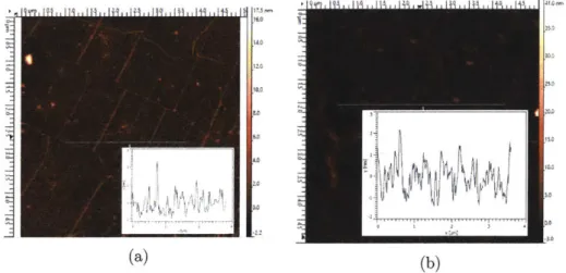
PMGI is chosen instead of PMMA because it results in a cleaner film. The AFM images in Figure 2.2 show the resulting film after each resist treatment. Four pieces of Si/SiO2/Graphene samples were purchased from ACS Material. One piece was used as the
control set where no resist was applied. The remaining tree samples were spin-coated with PMMA, MMA and PMGI respectively. Then samples coated with PMMA and MMA were exposed under 220nm deep UV light to make the film dissoluble in developer and then immersed in diluted Methyl isobutyl ketone (MIBK) solution. The sample with PMGI was immersed in MICROPOSIT CD-26 developer. All samples were rinsed with Acetone and Isopropyl alcohol and dried with nitrogen gun. Shown in Figure 2.2 is the resulting
Figure 2.1: Schematics for PMGI/SPR700 bilayer Patterning Process. Green film repre-sents PMGI and orange film reprerepre-sents SPR700
AFM images of the samples after their treatments. The circled dots are large particles on graphene surface. Since there are such particles on the bare graphene sample, it is possible that those particles are originated from the source of the graphene film instead of the resist treatments. From the Phase images it is easy to see that that PMGI treatment gives the cleanest film while PMMA treatment ends up with lots of contamination. Table 2.1 lists the surface roughness of the graphene samples after their treatment. Sample with PMGI has the lowest average roughness while PMMA has the highest. It also seems like PMGI treatment may be able to clean the graphene surface, since the roughness is even lower than that of bare graphene.
Even though PMMA tends to leave residues on graphene surface, it is still the most common supporting film for 2D materials wet transfer methods. Typically acetone is used to remove PMMA after transfer but there are still many particles left according to the AFM images. N-Methyl-2-Pyrrolidone (NMP) is a much stronger solvent comparing to acetone. Figure 2.3(a) shows the graphene film after exposure to PMMA and Figure 2.3(b) shows the same film after an overnight immersion in room temperature NMP. It is clear to see that the film was much cleaner after the NMP treatment. The surface roughness is even smaller than that of PMGI treatment. However, NMP can be too aggressive and actually damage graphene. NMP heated at 600C will tear the graphene film completely. If there are large particles prior to NMP treatment, it is possible that room temperature
Treatment Bare PMMA MMA PMGI
Height
Phase
Figure 2.2: AFM Images of graphene films onSiO 2 substrate with different photoresist treatments
NMP will lift up the particles too quickly and lead to a local tear on the graphene film. Figure 2.3(c) is a microscope image showing the damaged graphene patterns after NMP treatment. To keep the graphene film clean and undamaged, acetone or developer can be used to first remove large portion of the polymer film. NMP treatment can be added in the last step to clean small residues.
Table 2.1: Surface roughness of graphene film after different treatment
Ra [nm] Rq [nm] Bare 0.583 0.769 PMMA 0.921 1.26 MMA 0.520 0.764 PMGI 0.425 0.268 PMMA + NMP 0.395 0.695
In summary, PMGI/SPR700 bilayer stack was developed to pattern graphene using standard photolithography. PMGI is chosen as the protection layer to keep graphene as clean as possible. In addition, room temperature NMP bath can help remove small residues from PMMA, MMA and PMGI films during fabrication process. This method also works for patterning and maintaining the cleanness and integrityof MoS2 films.
:::__~~~- - __ - -
-60 pm
0.D hase g pm
(a) (b)
Figure 2.3: Effect of NMP Treatment with PMMA Processed Graphene film on SiO2
substrate. (a) PMMA processed graphene, (b) PMMA processed graphene after NMP overnight, (c)microscrope image of patterned graphene film after NMP treatment
2.2
Passivation
The high surface-to-volume ratio of 2D materials make them very sensitive to environmen-tal changes. It is one of the qualities that makes them ideal as sensing materials. However, it also means the device behavior can change upon exposure to unwanted but common molecules in ambient environment such as water and oxygen. Such changes will make the device non-predictable and it is non-ideal for sensor applications. One solution to this issue is to passivate the 2D material surface from direct exposure to the environment.
High-k dielectric thin films like aluminum oxide (Al203) and hafnium oxide (HfO2) have already been used as passivation layer in silicon technology. The standard technology to deposit such films is atomic layer deposition (ALD). ALD consists of two self-limiting surface reactions. The growth substrate is exposed to alternating pulses of precursor and oxidant with a purge step in-between. Each cycle deposit a monolayer of the material with high uniformity. The film thickness is easily controlled by the number of cycles.
-j
Comparing to other deposition methods involving high energy species such as sputtering, ALD is less aggressive and can potentially reduce the damage on the 2D material films during deposition.
In spite of the great potential of ALD films to passivate 2D materials, the absence of out-of-plane dangling bonds in 2D materials make it difficult to initiate ALD growth [71]. As shown in Figure 2.4, direct ALD growth on grpahene andMoS2 resulted in
islands of dielectric dots instead of a continuous film. The roughness of such films are normally larger than 1nm [78, 76]. The preferential growth of dielectric film mostly happens on defect sites, grain boundaries and wrinkles on the 2D film. This is due to the lack of functional dangling bonds on the basal plane. Density functional theory (DFT) calculation shows that various ALD precursors tend to absorb physically on the graphene basal plane [71]. Chemical adsorption of precursor molecules on graphene is unlikely due to the high activation barriers. The low probability of chemical absorption makes ALD nucleation process more difficult[78, 71]. Defect sites, grain boundaries and winkles however, are more active and easier for precursors to absorb chemically. Similar behavior was observed with 2D TMD materials such asMoS2. XPS shows weak interaction between
MoS2 surface and hafnium precursor during standard Hf02ALD process [47]. To enable
(a) (b)
Figure 2.4: AFM images of ALD dielectric on (a)graphene and (b)MoS2. Figures adopted from [76] and [78]
uniform ALD deposition, nucleation sites need to be added on 2D film surface intentionally to promote chemical absorption of precursors. This could be done by directly modifying the film surface or by depositing a seed-layer prior to the ALD process. Oxygen, ozone and nitrogen plasma treatment can convert part of the sp2
out-of-plane sp3 bonds to create oxygen or nitrogen containing surface groups [71].This method however, can result in degradation of charge carrier mobility due to the disruption of the sp2 backbone of graphene. By depositing a thin layer of polymer or metal film as the seeding layer can avoid the damage of 2D materials. Perylene tetracarboxylic acid coating was firstly used by Wang et al. to achieve uniform A1203 ALD deposition on graphene [74]. The polymer seeding method typically results in a slightly reduction in carrier mobility due to additional phonon scattering introduced by the polymer layer. In addition, a 1.5-42.5V right shift of Dirac point was observed in some of the graphene FETs using polymers seeding layer[71]. A metal seed-layer can be used to avoid p-doping the graphene channel. Kim et al. demonstrated an uniform deposition of 15nm A1203 on
graphene using a thin Al seeding layer. High mobility (8600 cm2V-Is-1) and near-zero Dirac point (0.08V) was achieved after the deposition, indicating minimal damage and doping on graphene film [36].
In this project, we chose to use Al as the seeding material and ALD A1203 as the
passivation layer to avoid doping of the channel. Specifically, 2nm Al thin film is deposited on the device using electron beam evaporation. The device is then baked at 150°C for 10 minutes in ambient air to fully oxidize the Al film. 150 cycles of ALD process at 120°C with trimethylaluminum(TAM) and water as precursors are used to deposit roughly 15nm of A1203. The results is shown in Figure 2.5. The oxide film is uniform on both graphene
and MoS2. The average roughness is 0.37nm for graphene and 0.42nm MoS2 over 5
micrometers.
One of the reasons to have a passivation layer is to mitigate the hysteresis in measure-ment. Shown in Figure 2.6(a) is a typical I- V characteristic for electrolyte-gated graphene field-effect transistors (FETs). The source-drain current (Ids) is measured with respect to a double-sweep of gate voltage (Vg,).There are generally two mechanisms that may cause the hysteresis: charge transfer and capacitive gating [72]. When a total charge of Aq is transferred in/from graphene, it will cause a positive shift in conductance AV = Aq/C,
where C is the capacitance of the dielectric [72]. The capacitive gating effect will increase the carrier density in graphene due to the enhancement of local electrical field [72]. This
(a) (b)
Figure 2.5: AFM images of ALD A1203 on (a)graphene and (b)MoS2 surface with Al as
the seeding layer
acts as an additional gating thus leading to an negative shift. In electrolyte-gated con-figuration, the capacitive gating is generally more dominant. As shown in Figure 2.6(a), an slightly negative shift in the Dirac point is present between the forward-sweep and backward-sweep. There is also a right-shift of the I-V curve between two consecutive mea-surements. This could be from the adsorbed water molecule on graphene surface,where electrons are transferred from graphene to the adsorbed water layer, resulting in hole doping (right shift) of graphene [55]. By having an oxide passivation layer, the hysteresis can be suppressed. As shown in Figure 2.6(b), no hysteresis is present between forward and backward sweep as well as between consecutive measurements in samples passivated with ALD A1203. A possible explanation could be that the oxide layer protects graphene
from water molecule and other surface absorbents. By having a high-quality dielectric film with the help of seeding layer, the interface between the oxide and graphene could be more stable and less likely to have interface traps. It is also important to note that hysteresis is depended on the voltage range, sweeping rate and surrounding condition [72]. The data in Figure 2.6 were measured under the same range (-.7V to 0.7V), rate (lOmV/s) and environment for fair compassion.
To further investigate the effect of oxide passivation on electrolyte-gated graphene FETs, the I-V curves from before and after oxide deposition are plotted on the same axis as shown in Figure 2.7. The source-drain current decreased by roughly a factor of 1.5 at the
3.5p 1156p Sweep 1 1Sweep 1 Sweep 2 Swee 2 3.0Op 1.43p --2.5p - 1.30p-2.0 1.17P 1.5p1.04pi 1.011 910.001" ____________________ -0.8 -0.8 -0.4 -0.2 0.0 0.2 0.4 0.6 0.8 -0.8 -0.6 -0.4 -0.2 0.0 02 0.4 0.8 0.8 Vgs(v) Vgs(V) (a) (b)
Figure 2.6: (a)Hysteresis of electrolyte-gated graphene FETs without A1203 passivation
(b)hysteresis of electrolyte-gated graphene FETs with A1203 passivation
Dirac point after the oxide is deposited. If we consider the capacitance between graphene and the gate, there are mainly two contributions for devices without oxide: quantum capacitance of graphene due to its density of state and the double-layer capacitance at the electrolyte-graphene interface. With the additional dielectric passivation layer, there is a third component: oxide capacitance. The double-layer capacitance is roughly 10-20
pF/cm2 for common salt electrolyte [75, 43]. The quantum capacitance of graphene is given by the following equations [43]:
C = 2q2 (InG - n 1)1/2 (2.1)
hvF#
qVch )2(2)
hvFf
where q is the electron charge, h is the reduced Plank constant, VF is the Fermi velocity, nG
is the carrier concentration induced by gate voltage, n* is the effective charged impurity concentration and Vch is the electrical potential on graphene channel. Since the quantum capacitance depends on the electrical potential, it has a minimum value at the Dirac point. The theoretical CQ,inis roughly 0.8 pF/cm2 but the experimental value is in the range of 1-10 tF/cm2 depending on the graphene quality and electrolyte condition[75, 43]. For 15nm of A1203, the capacitance is about 0.5 pF/cm
2. By having an additional small
should be lower. Since the Ida, is proportional to square-root of total capacitance [43], the oxide-passivated device will have an decrease in channel current. The measurement in Figure 2.7 was taken using water as the solution gate. Taking into account the double-layer capacitance of water (- 20pF/cm2) and CQ,, (~ 1
pF/cm2 for diluted electrolyte [22]) as well as oxide capacitance (~ 0.5 pF/cm2), the ratio of Ids,min between devices
with and without oxide is about 1.7.
3.Op -2.Op 1.0p -0.8 -0.6 -0.4 -0.2 0.0 0.2 Vgs (V) 0.4 0.6 0.8
Figure 2.7: Effect of A1203 passivation on electrolyte-gated graphene FETs' I-V
charac-teristic
The leakage current (gate current Ig,), however, was 3 orders of magnitude smaller for oxide-passivated device. Low leakage current is good for avoiding reaction in the elec-trolyte. The Dirac point also changed from near-zero to a more negative value, indicating a slight n-doping effect from A1203 on graphene film. Another issue to note is that the
V-shaped curve is less "sharp" with the oxide passivation. The channel conductance is less "responsive" to the change in electrical potential, which is non-ideal for a chem-resist type of sensors. In fact, the oxide film could also introduce additional charge traps that hinder the device performance if the oxide quality is low due to undesired chamber pres-sure or temperature. In a latter section we will talk about the importance of surface
ids no oxide
in-Ids with oxide
--Igs no oxide Igs with oxide
-r - -V/ 1 00n - 10n riOn in lop -10p.P 1 p *lOOf
functionalization. Some functionalization can cover the sensing surface in a uniform and insulating way so that the functionalization can act like a passivation layer. In this case, it is not necessary to add an extra layer of oxide.
Even for sensing applications that does not require oxide at the sensing area, passiva-tion at the contacts is still needed in order to protect the contacts from corrosive solupassiva-tion. Polymers such as SU-8 can be used to passivate the device while leaving the sensing area open the electrolyte. The hydrophobicity of such polymer can also promote analyte in solution to reach the sensing material. Previous research has shown that a recessed SU-8 passivation on graphene electrolyte-gated field-effect transistors can improve transconduc-tance performance [43]. It also shows SU-8 passivated device may be biased over a wider range of V, values while still having near-optimal transconductance [43]. The maximum leakage current can also be reduced to 10s of nA. Shown in Figure 2.8 is the sensor re-sponses of two devices. The two devices went through the same fabrication process except for the passivation layer. The device in Figure 2.8(a) is passivated with 500nm of SU-8 with the sensing area open. The device in Figure 2.8(b) is passivated with 15nm of A 203.
Two consecutive measurements were taken at each concentration for both devices. The black dots indicates first measurements and the red dots are the second measurement. It is clear that the device oxide passivation has a large variation between two measure-ment while the device with no oxide passivation has almost no difference. In this case the functionalization is a thick polymer film that already provides enough passivation for graphene from the solution. Adding a oxide layer not only reduces the current reading due to the oxide capacitance, but could also induced additional impurities that eventually increases the hysteresis of the device. Therefore, for sensors similar to Figure 2.8, SU-8 passivation is more suitable than oxide passivation.
Comparing to graphene,MoS2 has shown more severe hysteresis in unprotected films.
Shown in Figure 2.9(a) is the output characteristics of a back-gatedMoS2 FET without
oxide passivation. The hysteresis between forward and backward sweep is very large.The
Ids starts to decrease after device reaches the saturation region. This indicate severe degradation of theMoS2 in ambient environment.Shown in Figure 2.9 (b) is the output
0.66 A10041719 0.64- A041119 02. • 2ndsweep 0.62 1
e2ndsweep
0.60- 0,20 -0.58I
0.56 _0,15 . 00.54T 0.2 0. 10 -0.52 -0.46 -0 --6 -5 -4 -3 - -1Log(concentration) Log(concentraion) FuncFunctionaation SU-8 S U-8 A203 (a) (b)Figure 2.8: Sensor response and structure of device (a) SU-8 passivation and (b) with oxide passivation
characteristic of oxide-passivatedMoS2. The hysteresis is drastically reduced and no
degradation is observed at high voltage. The transfer characteristic of non-passivated MoS2 devices is shown in Figure 2.9(c). The hysteresis between forward and backward
sweep is roughly 0.5V. The hysteresis between two sweeps is about 0.25V. The on/off ratio is 103, which is much lower than that of typical MoS2 based transistors.
With oxide passivation, the hysteresis of forward and backward sweep is still present but the hysteresis between two sweeps is suppressed. The clockwise hysteresis in the transfer characteristic can be explained by the trap-filling phenomenon [34]. In forward sweep, negative bias pushes electrons trapped at the interface into the MoS2 channel. The
interface traps are then positively charged, leading to a negative shift of the curve. When a more positive bias is applied at the backward sweep, the electrons injected into the trap states and the traps become neutral, shifting the curve to a more positive position.
Since an oxide below a top gate will not mitigate the charge traps in the back-gate dielectric, it is expected that same type of hysteresis is still present in passivated device. The on/off ratio of passivated device increases to 106, which is comparable to the values in literature. However, the sub-threshold swing (SS) decreased from 190 mV/dec to
250.On - 100.01 - -Vgs = -1V --- VgsOV <1.5x 200.0n - 5x -SO 01.5op - ~. 100.0n - -- Vgs = V 40.011 -Vgs = 2V 50.0n - -Vgs - 3V 20.Op -0.0 . 0.0- '--0.1 0 0.1 0. 0.3 0.4 0.5 0.6 0.7 0.8 0 1 2 3 4 Vds (V) Vds (V) (a) (b) •Sweep 1I Sweep 1 10n - eSweep 2 1p - Sweep 2 ilon 1On ino 100p.p lp -100p -0.5 0.0 0.5 1.0 -7.5 -7.0 -8.5 -6.0 -5.5 -5.0 -4.5 -4.0 Vgs () Vgs () (c) (d)
Figure 2.9: I- V Characteristics of MoS2 Back-gated Transistors.(a) Output characteristics
without oxide, (b)output characteristics with oixde, (c) transfer characteristics without oxide, (d) transfer characterstics with oxide
442 mV/dec. Also, the threshold voltage (VT) changed from near OV to below -7V. This is highly undesirable for sensing application. Ideally, MoS2 FETs should have a
sub-threshold region near V with a sharp SS. In this way, a slight change in electrical potential due to analyte will result in a large change in source-drain current.
We showed that ALD A1203 on MoS2 could protect the film from ambient environment
thus reducing device degradation and hysteresis. It is also important to investigate other passivation methods to reduce hysteresis while keep the sub-threshold region to near OV with a sharp sub-threshold swing. Shown in Figure 2.10 is the transfer characteristics of MoS2 transistors with different types of passivation layer conducted by Yu et al. [78]. For
300
nO ADO,+ ALD A,0, 200 150 0 niol 100 601 20 101 4-2 0 2 4 6 1 3 4 S 6
a
, , , 1 5 ..., , 7 TCNQ+NPC 0 06 6 + ALD A,03 10 / 010 3 1-0 1 0 0~~~0.1
.. -- 2 0 2 4 6 -3-2-1 0 1 2 3 4 5 6 vTG(v) vG(v) m a 10 10 315FNl 101 A10 1 10 -2 0 2 4 6 • 1 2 3 4 5 --140 101 10. .1 .L .A.10.. so-2 0 40 40 10t 0L 0 9~40
10' 20 -0' - V -2 0 2 4 1 4 6 vT6(v) vTG(v)Figure 2.10: Transfer characteristics of MoS2 based transistors with different types of passivation. Figure adopted from Yu et al. [78].
that it could mitigate the n-doping effect of A1203 layer well still keep the current and SS
as high as possible [78].
2.3
Conclusion
In this chapter, we introduced a new method to pattern 2D materials with cheap and faster photolithography instead of expensive and slow electron beam lithography. PMGI was determined to be the best resist to keep the graphene free of residues. Bilayer stacks of PMGI/SPR700 can be used as the etch mask for graphene patterning process. Room temperature NMP can effectively clean the graphene surface after fabrication.
The second part of the chapter discussed the passivation technology for 2D films. A thin layer of Al metal needs to be deposited on the 2D film prior to ALD deposition. A high-quality and uniform A1203 can successfully passivate both graphene and MoS2 surface from contamination in the ambient environment. We demonstrated that A1203
passivation layer can effectively reduce hysteresis and reduce leakage. However, oxide
film can also induce additional charge traps or doping effect on graphene andMoS2. In
practice, the passivation material needs to chosen carefully with full consideration of the actual requirement of the application.
Chapter 3
Graphene-based Biosensors
3.1
Electrolyte-gated graphene field-effect transistors
Our body generates many types of fluids such as sweat, tears, urine and blood. These body fluids contains numerous molecules that indicates the status of our health. Many chemical and biological sensors that have been developed over the years are aimed at detecting those biomarkers in their original fluid state. Therefore, electrochemical sensing is a large field within the sensor family. However, these sensors typically require bulky measurements instrument such as potentiostats and experienced professionals to run and analyze the collected data. An FET-based sensor approach is cheaper and less bulky. With a simplified readout system, it is more suitable for realization of easy-to-use health monitoring system. Graphene is well-suited for electrochemical measurement due to its wide electrochemical potential window of 2.5V in O.1M Phosphate-buffered saline solution
(PBS) [84].
Graphene electrolyte-gated field-effects consist of a sheet of graphene channel with two metal contact:source contact and drain contact. The sensing area is directly exposed to the electrolyte environment. An Ag/AgCl reference electrode is typically used to apply stable gate voltage. Passivation layers is normally used to protect the contact while leaving the graphene exposed to the electrolyte. The device structure and measurement setup of a typical electrolyte-gated graphene FET is shown in Figure 3.1(a). When the gate-electrode is interfaced with the electrolyte, an electrical double layer is formed. Cations
or anions in the electrolyte migrate to the surface of the electrode due to the potential applied by the gate. In equilibrium, the ionic charge is screened by an equal and opposite amount of charges in the electrode and thus charge neutrality is achieved. Since the charge separation occurs over only a few nanometers, the electric double layer capacitance is fairly large. Large gate capacitance combining with graphene's high mobility promises graphene electrolyte-gated FETs with large-transconductance and high sensitivity towards change in electrolyte environment.
s s
(a) (b)
Figure 3.1: (a)Device structure and measurement setup for electrolyte-gated graphene field-effect transistors. (b)Three most common models to describe electric double layers, figure taken from [36]
3.2
pH sensing
To demonstrate the sensing ability of graphene electrolyte-gated FETs, the device is tested with buffer solution with different pH values. Specifically, the fabrication process starts with a silicon substrate with 300nm of Si02. A layer of Ti/Au (5nm/100nm) metal stack is deposited using electron beam deposition as the source and drain measurement pads. The metal pads are kept away from the actual sensing area in order to leave a clean and flat area for graphene transfer. Oxygen plasma is used to clean and prepare the surface for transfer. Graphene film is obtained by ACS Material. ACS Material provides a type of graphene product called Trivial Transfer Graphene. Instead of the typical copper/graphene/PMMA structure of most commercial CVD graphene product, Trivial Transfer Graphene has a polymer/graphene/PMMA structure. Water can easily
![Figure 1.1: The family of 2D materials. Figure adopted from [1]](https://thumb-eu.123doks.com/thumbv2/123doknet/14278158.491286/13.917.207.699.212.526/figure-family-d-materials-figure-adopted.webp)


![Figure 2.4: AFM images of ALD dielectric on (a)graphene and (b)MoS 2 . Figures adopted from [76] and [78]](https://thumb-eu.123doks.com/thumbv2/123doknet/14278158.491286/26.917.197.719.664.868/figure-afm-images-ald-dielectric-graphene-figures-adopted.webp)