DOI: 10.1007/s00340-007-2760-1
Rapid
communication
Lasers and Optics
d.j.h.c. maas a.-r. bellancourt b. rudin m. golling h.j. unold t. s ¨udmeyer u. kelleru
Vertical integration of ultrafast
semiconductor lasers
Department of Physics, Institute of Quantum Electronics, ETH Zurich, Wolfgang-Pauli-Str. 16, 8093 Zurich, Switzerland
Received: 6 August 2007
Published online: 22 August 2007 • © Springer-Verlag 2007
ABSTRACT Lasers generating short pulses – referred to as ultrafast lasers – en-able many applications in science and technology. Numerous laboratory experiments have confirmed that ultrafast lasers can significantly increase telecommunication data rates [1], improve computer interconnects, and optically clock microprocessors [2, 3]. New applications in metrology [4], supercontinuum generation [5], and life sciences with two-photon microscopy [6] only work with ultrashort pulses but have relied on bulky and complex ultrafast solid-state lasers. Semiconductor lasers are ideally suited for mass production and widespread applications, because they are based on a wafer-scale technology with a high level of integration. Not surprisingly, the first lasers entering virtually every household were semiconductor lasers in compact disk play-ers. Here we introduce a new concept and make the first feasibility demonstration of a new class of ultrafast semiconductor lasers which are power scalable, support both optical and electrical pumping and allow for wafer-scale fabrication. The laser beam propagates vertically (perpendicularly) through the epitaxial layer structure which has both gain and absorber layers integrated. In contrast to edge-emitters, these lasers have semiconductor layers that can be optimized separately by using different growth pa-rameters and with no regrowth. This is especially important to integrate the gain and absorber layers, which require different quantum confinement. A saturable absorber is required for pulse generation and we optimized its parameters with a single self-assembled InAs quantum dot layer at low growth temperatures. We refer to this class of devices as modelocked integrated external-cavity surface emitting lasers (MIXSEL). Vertical integration supports a diffraction-limited circular output beam, transform-limited pulses, lower timing jitter, and synchronization to an external electronic clock. The pulse repetition rate scales from 1-GHz to 100-GHz by simply changing the laser cavity length. This result holds promise for semiconductor-based high-volume wafer-scale fabrication of compact, ultrafast lasers.
PACS42.55.Px; 42.55.Xi; 42.65.Re; 78.47.+p; 78.67.-n; 78.67.Hc
1 Introduction
The vertical external cavity surface emitting laser (VECSEL) [7] has recently gained much interest be-cause of its power scaling potential. In a VECSEL, the light is emitted in a per-pendicular direction through the epitax-ial surface, in contrast to edge-emitting lasers, where the beam propagates in u Fax: +41 44 633 10 59, E-mail: [email protected]
the epitaxial layers. An important ad-vantage of optically pumped VECSELs is that they can convert fairly low-cost, low-beam-quality optical pump power from high-power diode laser bars into a near-diffraction-limited output beam with good efficiency, in wave-length regions that are not covered by established solid-state laser gain mate-rials. CW output powers of up to 30 W
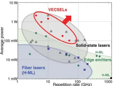
with a beam quality factor M2 of 3 have been reported from such optically pumped VECSELs [8], and electrically pumped devices have reached 0.5 W single transverse mode output power (i.e. M2= 1.1) [9]. To date, ultrafast VECSELs [10] have been successfully reported (Fig. 1) with average output powers of up to 2.1 W [11], pulse rep-etition rates of up to 50 GHz [12] and pulse durations as short as 477 fs [13]. All these results had diffraction-limited, circular output beams. These ultrafast VECSELs (see Fig. 2a) have at least three cavity elements, the gain struc-ture, the output coupler and a semi-conductor saturable absorber mirror (SESAM) [14, 15] for the generation of ultrashort pulses. Since VECSELs are semiconductor lasers, the integration of a semiconductor saturable absorber in the gain structure should be feasible even though a straightforward integra-tion from the separate device elements does not work and a new concept had to be developed. We refer to this new class of devices as modelocked inte-grated external-cavity surface emitting lasers (MIXSELs).
Semiconductor lasers have a num-ber of compelling advantages com-pared to other choices of laser ma-terial: the lasing wavelength can be tuned over a broad range by choos-ing the material composition, and the parameters determining the laser dy-namics can be precisely engineered (e.g. recovery time, saturation energy). They are well-established in the opti-cal communication market as reliable optical sources, and can have very low fabrication costs. So far, only ultra-fast edge-emitting semiconductor lasers
FIGURE 1 Output power for different types of ultrafast lasers operating in the gigahertz regime (1 GHz= 109Hz). To date the available laser sources in this regime are either based on edge-emitting
semiconductor lasers, harmonically modelocked (H-ML) fiber lasers, diode-pumped ion-doped solid-state lasers or vertical external cavity surface emitting semiconductor lasers (VECSELs). Above 100 GHz, the high-average-power edge-emitting lasers are also harmonically modelocked
have been fully integrated in one wafer. The highest output power to date is 250 mWat 4.3 GHz [16]. Unfortunately, such high average power cannot be ex-tended to pulse repetition rates well above 10 GHz because gain guiding at higher current densities gives rise to higher-order transverse modes. In addition, edge-emitting semiconductor lasers have strongly asymmetric beam profiles, which often need to be cor-rected with precisely mounted lenses. Typically, the same epitaxial layer forms both the gain (with a forward-biased section) and the saturable absorber (with a reverse-biased section) – and can therefore not be optimized indepen-dently. The long interaction length in the device introduces significant disper-sion and nonlinearities. It is also chal-lenging to fabricate an edge-emitting laser cavity length with a very precise pulse repetition rate and have this laser synchronized to an external reference clock.
Other interesting ultrafast lasers are either based on diode-pumped solid-state lasers or fiber lasers. Solid-solid-state lasers modelocked with SESAMs have increased pulse energy by three orders of magnitude, to more than 10µJ at multi-MHz repetition rates, increased pulse repetition rates by more than two orders of magnitude to 160 GHz, and reduced pulse duration into the sub-10-femtosecond regime [17–19]. However, gain material and absorber material are different and can not be manufactured
simultaneously, which results in higher complexity and costs. Moreover, dir-ect eldir-ectrical pumping is not feasible. Modelocked fiber lasers are not funda-mentally modelocked at high repetition rates. Instead, harmonic modelocking (H-ML) is used, where multiple pulses simultaneously circulate in the cavity at once, which is susceptible to pulse drop out and higher noise levels.
The MIXSEL is a fundamentally modelocked laser, in which only one pulse is circulating in the resonator (Fig. 2b). Every time the pulse hits a par-tially transmissive mirror, the output coupler, a small fraction is transmitted. The output beam consists of an equidis-tant pulse train with a period defined by the round-trip time of a pulse inside the laser cavity. The gain section inside the MIXSEL semiconductor structure amplifies the pulse, and a saturable ab-sorber section initiates and stabilizes the pulse formation. Such a saturable ab-sorber has a constant loss for cw-lasing, whereas pulses with high peak powers are able to saturate the absorber and therefore reduce its loss.
The semiconductor gain structure (Fig. 2a) contains a highly reflective (HR) mirror, a gain section, and an anti-reflective (AR) coating which provides low transmission loss from the semi-conductor device to the external cavity. Its gain section contains quantum wells (QWs), thin layers (for example, 10 nm) of semiconductors surrounded by bar-rier materials with larger potential
en-FIGURE 2 Integration scheme, progressing from conventional VECSEL-SESAM modelock-ing with (a) large mode area ratios and thus large cavities, (b) to absorber-gain integration in a modelocked integrated external-cavity surface emitting laser (MIXSEL). The MIXSEL semicon-ductor wafer structure contains two high reflectors (HR), quantum dot (QD) saturable absorber, quan-tum well (QW) gain and an anti-reflective (AR) coating. The first HR reflects the laser light and forms the laser cavity together with the external output coupler. The second one, the intermediate HR, is to prevent the pump light bleaching the saturable absorber
ergy (i.e. a larger bandgap) that confine electrons and holes inside the QWs. The gain structure is used as an amplifying mirror mounted onto a heat sink. Be-cause the beam diameters are typically larger than the total device thickness, the gain structure has an almost perfect one-dimensional heat flow, which al-lows power scaling: doubling the mode size doubles the output power [20] but maintains approximately the same tem-perature rise in the pumped material. The mode size can be easily adjusted with the output coupler.
The semiconductor saturable ab-sorber is responsible for self-starting and maintaining modelocking [17]. To date, the saturable absorber has been integrated into a separate mirror struc-ture device (i.e. the SESAM) and typic-ally used QW-absorbers with a bandgap slightly smaller than the photon en-ergy to absorb the intracavity light and generate a self-amplitude modulation (saturable absorption). When most pos-sible states for the excited electrons are occupied, the absorption becomes saturated which then reduces the loss. A SESAM has three important
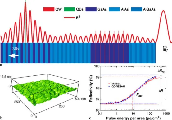
param-FIGURE 3 MIXSEL design. (a) Simulated electric field intensity inside the MIXSEL structure. The QD absorber layer is integrated in a “resonant structure” which means that we have an E-field enhancement in the absorber layer compared to the gain layers. The structure is grown with molecular beam epitaxy (MBE) on a GaAs substrate and is approximately 8µm thick (see Sect. 2 for more details). (b) AFM topography of the QD absorber layer (measured with a standard AFM tip radius of 10 nm) grown under the same conditions as in the MIXSEL but without any cover layer and without annealing (i.e. QD layer was grown at 430◦C with≈ 2 monolayer InAs deposition). (c) Nonlinear reflectivity measurement at a center wavelength of 957 nm at room temperature of an annealed resonant QD-SESAM (blue) and a full MIXSEL (red) with the same QD layer (in both cases grown at 400◦C). Under these conditions, the quantum wells in the MIXSEL structure did not absorb. We measured a saturation fluence Fsatof 9µJ/cm2resp. 11µJ/cm2, a modulation depth∆R of 2.5% resp.
2.6% and a nonsaturable loss ∆Rnsof 1% resp. 0.9% for the MIXSEL resp. QD-SESAM. The measurement wavelength was slightly detuned from resonance
with a lower electric field enhancement in the absorber (i.e.≈ 2.5 instead of 4). Here we clearly show that the additional growth of the MIXSEL structure does not degrade the saturable absorber parameters which would result in a significant increase in nonsaturable loss∆Rns
eters: the modulation depth, which is the difference in reflectivity between an unsaturated and a completely sat-urated SESAM, the saturation energy, which is the pulse energy needed to obtain a roll-over of the reduction in loss with higher pulse energies, and the nonsaturable absorption, which intro-duces a residual loss even when the absorber is fully saturated. The satura-tion energy depends on the mode size; if the area on the SESAM that we have to saturate becomes smaller, we need less pulse energy to saturate it. High-power ultrafast VECSELs are typically based on QW-SESAMs, with properties similar to the QWs in the gain struc-ture, which means similar saturation conditions. For stable modelocking, the absorber needs to saturate earlier and re-cover faster than the gain [19], and we have to choose a smaller spot size on the SESAM than on the gain structure (Fig. 2a). However, integration of such a QW absorber into the gain structure (Fig. 2b) is not possible due to the differ-ent mode areas.
With quantum dot (QD) saturable absorbers, we can resolve the satura-tion issue. Compared to QWs, QDs con-fine the electrons in all three dimensions (and are therefore referred to as dots). This reduces the density of states and can lower the required optical intensity for band filling if the oscillator strength does not change. In addition, with the dot density and the optical design of the structure (moving from an antiresonant to a resonant design, see Fig. 3a) [21] we can further reduce the saturation en-ergy and keep the modulation depth to the 1%-level. This is not possible with quantum well absorbers, because the re-quired reduction of the saturation flu-ence by a resonant design would cause a too large increase of modulation depth (up to 11 times, see [21]).
Until recently QDs have been mainly optimized for different applications, such as for example for single-pho-ton emitters [22], for low-threshold emitters [23], for multi-QD-layers SESAMs [24], for cavity quantum elec-trodynamics [25] or for quantum
com-putations [26]. Here we operate in a completely different regime because we used low temperature (LT) MBE growth to obtain a fast recovery time. LT growth incorporates defect states that act as efficient traps for the excited electrons and therefore reduce their re-combination time (i.e. the recovery time of the saturable absorber). Normally self-assembled InAs QDs on GaAs are grown at a growth temperature of 500 to 550◦C and due to the 7% lattice mismatch between GaAs and InAs, the two-dimensional growth changes into a three-dimensional one after a deposi-tion of about 1.5 to 1.7 monolayers of InAs [27]. We typically grow our QD saturable absorbers at around 400◦C and a thickness of about two monolay-ers of InAs is sufficient for the formation of quantum dots (Fig. 3b). In addition, at lower growth temperatures the mo-bility of the In and As atoms on the GaAs surface is strongly reduced which lowers the material thickness thresh-old for QD formation. Such a QD sat-urable absorber layer is integrated into
FIGURE 4 Pulse characterization of the current result with 40 mW average output power. Left: auto-correlation with sech2-fit, right: optical spectrum, inset: microwave spectrum on a 10-MHz span with
100-kHz resolution bandwidth
the MIXSEL structure (Fig. 3a) with a stronger electric field enhancement in the QD absorber layer compared to the QW gain layers – we refer to this as the “resonant” design motivated by our previous SESAM design work [21]. This reduces the saturation fluence Fsat
of the saturable absorber to well be-low 10µJ/cm2 (Fig. 3c is measured slightly off resonance – at resonance we would obtain an even smaller satu-ration fluence). In comparison a stan-dard QW-SESAM in a nonresonant structure typically has a saturation flu-ence well above 10µJ/cm2 into the
100µJ/cm2regime [21]. Both QW- and
QD-SESAMs have a recovery time in the picosecond regime.
The development of the QD sat-urable absorber was the crucial step towards the MIXSEL. The MIXSEL cavity is shown in Fig. 2b, which is not to scale. The semiconductor device only adds about 10µm to the laser cavity length – so most of the laser cavity beam propagates in air (e.g. a 50 GHz pulse repetition rate corresponds to a cav-ity length of 3 mm). This could be re-placed with another transparent wafer with the semiconductor wafer glued to one side and an integrated curved out-put coupler on the other side [28]. We used an output coupler with a radius of curvature of 60 mm. The heat sink is cooled down to −10◦C using two peltier elements. The thick (i.e. 600µm) substrate has a poor thermal conduc-tivity, resulting in a high temperature increase (over 110◦C), ultimately lim-iting the output power. This problem also arises with VECSELs and is
usu-ally solved by growing the layers in reverse order and substrate removal (i.e. “upside-down” structure) [8, 20]. With-out the thick substrate, the temperature increase can be reduced (below 20◦C) allowing for substantially higher output power.
The cw pump source delivered 1.5 W at 808 nm and is focused to a circular pump spot with a radius of 80µm. The lasing wavelength can be tuned between 953 nm and 956 nm with an intracav-ity 25µm-thick fused silica etalon. This gives us some adjustments in the field enhancement ratio between absorber and gain and the cavity group delay dispersion. Stable modelocking was ob-tained with a 5.4-cm long straight cavity and a 0.35% transmission output cou-pler. The laser delivered 40 mW average power in 35 ps pulses at 2.8 GHz with a spectral full-width half-maximum (FWHM) of 0.11 nm (Fig. 4). Mode-locking was also observed without the etalon but with less stability. The limited output power and low optical-to-optical efficiency is caused by the high tempera-ture increase. Power, pulse duration, and pulse repetition rates can be improved in the future with an “upside-down” struc-ture based on the previous results with modelocked VECSELs.
With the “upside-down” structure, we have even less stringent growth re-quirements for the MIXSEL. In the cur-rent “right-side-up” growth, the QW gain section has to be grown after the QD layer grown at low tempera-ture, which introduces some defects. “Upside-down” growth would reduce such defects and enhance gain.
for laser testing was required and we could emphasize our efforts on the un-derstanding and optimization of the QD saturable absorber layer which was the crucial step towards the feasibil-ity demonstration of our integration concept. Currently we still have some growth inaccuracies which cause a large group delay dispersion that is responsi-ble for the longer chirped pulses. In-situ growth characterization can be used to obtain higher accuracy.
In conclusion, we have successfully demonstrated the first passively mode-locked VECSEL with both the gain and absorber integrated into a single semi-conductor structure. This new-class of passively modelocked semiconductor lasers could enable the realization of ro-bust, ultra-compact multi-GHz sources suitable for mass production. The sim-ple straight cavity geometry allows for very high repetition rates. Moreover, advanced heat management will re-sult in multi-Watt average output pow-ers as previously demonstrated in the former VECSEL-SESAM results [10]. The last step towards even lower-cost and more compact ultrafast semicon-ductor surface emitting lasers will be electrical pumping. This would result in devices ideally suited for many ap-plications such as telecommunications, optical clocking, frequency metrology, microscopy, laser display – anywhere where the current ultrafast laser tech-nology is considered to be too bulky or expensive.
2 Methods
2.1 MIXSEL design and growth
The QDs are grown at 430◦C, the QWs at 520◦C, and the rest of the structure is grown at 600◦C for less defects and high optical gain. This higher temperature does not affect the QWs, however it anneals the QDs. This annealing changes the dot composi-tion and size, resulting in a blue shift of the absorption and emission wave-length [29]. We could compensate for this by initially growing the QDs at a photoluminescence peak of 1100 nm, then annealing the devices to shift the absorption peak to around 950 nm to match our lasing wavelength. The rest of the structure is standard VECSEL
growth: the intermediate distributed Bragg reflector (DBR) consists of AlAs and Al0.2Ga0.8As, where both
materi-als do not absorb the pump light. The bottom DBR consists of 30 pairs of AlAs/GaAs. The gain section consists of seven In0.13Ga0.87Asquantum wells
with a thickness of 7 nm surrounded by GaAs barriers that absorb the pump light. Finally, the anti-reflective coating has the same material compositions as the intermediate DBR. In this resonant structure we embedded the QD-layer in-side aλ/2-thick “sub-cavity” inside the bottom DBR which gives the field en-hancement in the absorber layer. The QDs are embedded inside a 20-nm thick GaAs layer surrounded by AlAs with a total optical thickness ofλ/2 (Fig. 3a). We kept the GaAs-layer as thin as pos-sible to minimize residual absorption in GaAs. After the growth, we solder the sample to a copper heatsink.
2.2 QD-SESAM design
In Fig. 3c we show for com-parison the nonlinear reflectivity meas-urement of a resonant QD-SESAM for which we used the same growth con-ditions as for the MIXSEL structure, except that we used a slightly lower growth temperature of 400◦C. This QD-SESAM was again a resonant design with the λ/2 “sub-cavity” on top and the QD-layer embedded inside the thin GaAs (i.e. ≈ 20 nm) and thicker AlAs layers. After the growth, the structure was in-situ annealed for 5 h at 600◦C, which is similar to the annealing that occurs during the MIXSEL structure growth. Within the first hour of the annealing process, the PL wavelength changes by a total of 125 nm, then it changes linearly with time at 5 nm/h.
2.3 Nonlinear reflectivity measurements
The measured nonlinear re-flectivity of the MIXSEL and the QD-SESAM is shown in Fig. 3c. The details of the measurement set-up are described
by Haiml et al. [30]. For this measure-ment we used a passively modelocked VECSEL with a separate SESAM in a V-shaped cavity (Fig. 2a) with a pulse duration of 6 ps, a maximum average output power of 2 W and a pulse rep-etition rate of 1.5 GHz. The laser was chopped and focused to a spot radius of 5µm on the device under test and the center wavelength was at 957 nm.
ACKNOWLEDGEMENTSThis work was supported in part by the Intel Corpora-tion through a university sponsored research agreement, the European Network of Excellence “ePIXnet,” and ETH Zurich with the FIRST clean-room facility.
AUTHOR INFORMATION The first three authors contributed equally to this work.
REFERENCES
1 L.F. Mollenauer, P.V. Mamyshev, J. Gripp, M.J. Neubelt, N. Mamysheva, L. Gruner-Nielsen, T. Veng, Opt. Lett. 25, 704 (2000) 2 M.J. Kobrinsky, B.A. Block, J.-F. Zheng,
B.C. Barnett, E. Mohammed, M. Reshotko, F. Robertson, S. List, I. Young, K. Cadien, Intel Technol. J. 8(2), 129 (2004), avail-able at http://www.intel.com/technology/itj/ archive.htm
3 A. Bhatnagar, C. Debaes, R. Chen, N.C. Helman, G.A. Keeler, D. Agarwal, H. Thienpoint, D.A.B. Miller, “Receiver-less clocking of a CMOS digital circuit using short optical pulses,” presented at 2002 IEEE/LEOS Annual Meeting; Conference Proceedings, 15th Annual Meeting of the IEEE Lasers & Electro-Optics Society, Glas-gow, Scotland, 2002
4 Th. Udem, R. Holzwarth, T.W. Hänsch, Na-ture 416, 233 (2002)
5 P. Russell, Science 299, 358 (2003) 6 K. Ohki, S. Chung, Y.H. Ch’ng, P. Kara,
R.C. Reid, Nature 433, 597 (2005)
7 M. Kuznetsov, F. Hakimi, R. Sprague, A. Mooradian, IEEE Photon. Technol. Lett. 9, 1063 (1997)
8 J. Chilla, S. Butterworth, A. Zeitschel, J. Charles, A. Caprara, M. Reed, L. Spinelli, “High Power Optically Pumped Semicon-ductor Lasers,” presented at Photonics West 2004, Solid State Lasers XIII: Technology and Devices, in Proc. SPIE 5332, 2004 9 J.G. McInerney, A. Mooradian, A. Lewis,
A.V. Shchegrov, E.M. Strzelecka, D. Lee, J.P. Watson, M. Liebman, G.P. Carey, B.D. Cantos, W.R. Hitchens, D. Heald, Elec-tron. Lett. 39, 523 (2003)
10 U. Keller, A.C. Tropper, Phys. Rep. 429, 67 (2006)
11 A. Aschwanden, D. Lorenser, H.J. Unold, R. Paschotta, E. Gini, U. Keller, Opt. Lett. 30, 272 (2005)
12 D. Lorenser, D.J.H.C. Maas, H.J. Unold, A.R. Bellancourt, B. Rudin, E. Gini, D. Ebel-ing, U. Keller, IEEE J. Quantum Electron. QE-42, 838 (2006)
13 A. Garnache, S. Hoogland, A.C. Tropper, I. Sagnes, G. Saint-Girons, J.S. Roberts, Appl. Phys. Lett. 80, 3892 (2002)
14 U. Keller, D.A.B. Miller, G.D. Boyd, T.H. Chiu, J.F. Ferguson, M.T. Asom, Opt. Lett. 17, 505 (1992)
15 U. Keller, K.J. Weingarten, F.X. Kärtner, D. Kopf, B. Braun, I.D. Jung, R. Fluck, C. Hönniger, N. Matuschek, J. Aus der Au, IEEE J. Sel. Top. Quantum Electron. 2, 435 (1996)
16 J.J. Plant, J.T. Gopinath, B. Chann, D.J. Ripin, R.K. Huang, P.W. Juodawlkis, Opt. Lett. 31, 223 (2006)
17 U. Keller, Nature 424, 831 (2003)
18 G. Steinmeyer, D.H. Sutter, L. Gallmann, N. Matuschek, U. Keller, Science 286, 1507 (1999)
19 U. Keller, Prog. Opt. 46, 1 (2004)
20 R. Häring, R. Paschotta, A. Aschwanden, E. Gini, F. Morier-Genoud, U. Keller, IEEE J. Quantum Electron. QE-38, 1268 (2002) 21 G.J. Spühler, K.J. Weingarten, R. Grange,
L. Krainer, M. Haiml, V. Liverini, M. Golling, S. Schön, U. Keller, Appl. Phys. B 81, 27 (2005)
22 C. Santori, D. Fattal, J. Vuckovic, G.S. Solo-mon, Y. Yamamoto, Nature 419, 594 (2002) 23 H.Y. Liu, D.T. Childs, T.J. Badcock,
K.M. Groom, I.R. Sellers, M. Hopkinson, R.A. Hogg, D.J. Robbins, D.J. Mowbray, M.S. Skolnick, “High-performance three-layer 1.3-mu m InAs-GaAs quantum-dot lasers with very low continuous-wave room-temperature threshold currents,” IEEE Pho-ton. Technol. Lett. 17, 1139 (2005) 24 E.U. Rafailov, S.J. White, A.A. Lagatsky,
A. Miller, W. Sibbett, D.A. Livshits, A.E. Zhukov, V.M. Ustinov, IEEE Photon. Technol. Lett. 16, 2439 (2004)
25 K. Hennessy, A. Badolato, M. Winger, D. Gerace, M. Atatüre, S. Gulde, S. Fält, E.L. Hu, A. Imamoglu, Nature 445, 896 (2007)
26 Xiaoqin Li, Yanwen Wu, D.G. Steel, D. Gam-mon, T.H. Stievater, D.S. Katzer, D. Parker, C. Piermarocchi, L.J. Sham, Science 301, 809 (2003)
27 R. Leon, P.M. Petroff, D. Leonard, S. Fafard, Science 267, 1966 (1995)
28 M.W. Wiemer, R.I. Aldaz, D.A.B. Miller, J.S. Harris, IEEE Photon. Technol. Lett. 17, 1366 (2005)
29 S. Malik, C. Roberts, R. Murray, M. Pate, Appl. Phys. Lett. 71, 1987 (1997)
30 M. Haiml, R. Grange, U. Keller, Appl. Phys. B 79, 331 (2004)