HAL Id: hal-01742020
https://hal.archives-ouvertes.fr/hal-01742020
Submitted on 27 Mar 2018
HAL is a multi-disciplinary open access
archive for the deposit and dissemination of
sci-entific research documents, whether they are
pub-lished or not. The documents may come from
teaching and research institutions in France or
abroad, or from public or private research centers.
L’archive ouverte pluridisciplinaire HAL, est
destinée au dépôt et à la diffusion de documents
scientifiques de niveau recherche, publiés ou non,
émanant des établissements d’enseignement et de
recherche français ou étrangers, des laboratoires
publics ou privés.
Strain mapping of tensiley strained silicon transistors
with embedded Si1–yCy source and drain by dark-field
holography
Florian Hüe, Martin Hÿtch, Florent Houdellier, Hugo Bender, Alain Claverie
To cite this version:
Florian Hüe, Martin Hÿtch, Florent Houdellier, Hugo Bender, Alain Claverie. Strain mapping of
tensiley strained silicon transistors with embedded Si1–yCy source and drain by dark-field
holog-raphy. Applied Physics Letters, American Institute of Physics, 2009, 95 (7), pp.73103 - 73103.
�10.1063/1.3192356�. �hal-01742020�
Strain mapping of tensiley strained silicon transistors with embedded
source
and drain by dark-field holography
Florian Hüe, Martin Hÿtch, Florent Houdellier, Hugo Bender, and Alain Claverie
Citation: Appl. Phys. Lett. 95, 073103 (2009); doi: 10.1063/1.3192356 View online: https://doi.org/10.1063/1.3192356
View Table of Contents: http://aip.scitation.org/toc/apl/95/7 Published by the American Institute of Physics
Articles you may be interested in
Improved precision in strain measurement using nanobeam electron diffraction Applied Physics Letters 95, 123114 (2009); 10.1063/1.3224886
Dark field electron holography for quantitative strain measurements with nanometer-scale spatial resolution Applied Physics Letters 95, 053501 (2009); 10.1063/1.3196549
On the influence of elastic strain on the accommodation of carbon atoms into substitutional sites in strained Si:C layers grown on Si substrates
Applied Physics Letters 94, 141910 (2009); 10.1063/1.3116648
Measurement of incomplete strain relaxation in a silicon heteroepitaxial film by geometrical phase analysis in the transmission electron microscope
Applied Physics Letters 91, 231902 (2007); 10.1063/1.2821843
The addition of strain in uniaxially strained transistors by both SiN contact etch stop layers and recessed SiGe sources and drains
Journal of Applied Physics 112, 094314 (2012); 10.1063/1.4764045
An efficient, simple, and precise way to map strain with nanometer resolution in semiconductor devices Applied Physics Letters 96, 091901 (2010); 10.1063/1.3337090
Strain mapping of tensiley strained silicon transistors with embedded
Si
1−yC
ysource and drain by dark-field holography
Florian Hüe,1,a兲 Martin Hÿtch,1Florent Houdellier,1Hugo Bender,2and Alain Claverie1
1CNRS, CEMES, 29 rue Jeanne Marvig, F-31055 Toulouse, France and Université de Toulouse,
UPS, F-31055 Toulouse, France
2IMEC, Kapeldreef 75, 3001 Leuven, Belgium
共Received 5 June 2009; accepted 9 July 2009; published online 18 August 2009兲
Dark-field holography, a new transmission electron microscopy technique for mapping strain distributions at the nanoscale, is used to characterize strained-silicon n-type transistors with a channel width of 65 nm. The strain in the channel region, which enhances electron mobilities, is engineered by recessed Si0.99C0.01 source and drain stressors. The strain distribution is measured across an array of five transistors over a total area of 1.6 m wide. The longitudinal tensile strain reaches a maximum of 0.58%⫾0.02% under the gate oxide. Theoretical strain maps obtained by finite element method agree well with the experimental results. © 2009 American Institute of
Physics. 关DOI:10.1063/1.3192356兴
Strained-silicon channel technology is now implemented in all the latest generation of nanoelectronic devices.1,2 Straining silicon considerably increases the mobility of car-riers, either electrons or holes, leading to significantly en-hanced performances in metal-oxide-semiconductor field-effect transistors 共MOSFETs兲.3–5 Different techniques have been investigated to engineer strain in devices, for example the growth of relaxed virtual substrates to induce biaxial strain in the channel region, or the capping of transistors with a specially engineered high tensile stress silicon nitride layer to induce uniaxial tensile strain.6,7The most widely reported technique, however, is to use recessed Si1−xGex or Si1−yCy
sources and drains as stressors for compressive strain in
p-MOSFETs8 and tensile strain in n-MOSFETs,9,10 respec-tively. By combining these different methods, it is possible to induce various distributions of strain.11 Nevertheless, de-tailed knowledge of the exact strain distribution in two di-mensions is required to understand how improvements in performance can be optimized.
Transmission electron microscopy共TEM兲 is the most ap-propriate tool for measuring strains at the nanoscale. Convergent-beam electron diffraction12–14 and nanobeam diffraction15can be used to measure strain accurately at spe-cific points on the sample but are less suited for the mapping of strains continuously across devices. More recently, aberration-corrected high-resolution transmission electron microscopy 共HRTEM兲16 has been used to map strains in
p-MOSFET devices. Nevertheless, the method, although
promising, suffers from the limited field of view, sample preparation issues, and the inherently low signal-to-noise ra-tio of HRTEM observara-tions. To overcome these difficulties, we recently introduced an electron holographic technique for measuring strain共HoloDark兲.17,18The technique is based on the interference of diffracted beams from adjacent sample areas using the dark-field holography configuration.19Unlike conventional off-axis holography, the phase differences in
the diffracted beams give direct access to local changes in the lattice parameters.17
In this paper, we report on the analysis by dark-field holography of the strain distribution in n-MOSFETs with recessed sources and drains of carbon-doped silicon. The measurement of strain in such devices10,20,21 is more chal-lenging than for SiGe/Si systems, as the lattice mismatches are significantly smaller. We will also demonstrate a recent improvement in the precision and field of view of the tech-nique.
A series of dummy transistors with a channel width of 65 nm were prepared using Si0.99C0.01sources and drains stres-sors for the Si channel in an ASM Epsilon®2000 reactor.22 TEM samples were prepared by focus ion beam for 关11¯0兴 zone axis observations关Fig.1共a兲兴 to a thickness of about 150 nm. The optimized preparation method maintains a relatively thick region of substrate adjacent to the thinned outer edge and prevents the specimen from bowing and cracking.
Microscope observations were performed on the SACTEM-Toulouse, a Tecnai F20 共FEI兲 TEM operating at
a兲Present address: Department of Materials Science and Metallurgy,
Univer-sity of Cambridge, Pembroke Street, Cambridge CB2 3QZ, United King-dom. Electronic mail: fmh29@cam.ac.uk.
FIG. 1. 共Color online兲 Dark-field strain analysis of n-MOSFETs with em-bedded Si0.99C0.01sources and drains:共a兲 conventional TEM observation of
the structure,共b兲 dark-field hologram obtained by interfering the 共220兲 dif-fracted beams from areas A and B,共c兲 phase analysis of hologram revealing local changes of lattice parameter, and 共d兲 xx strain map with profile in channel from gate oxide to substrate共e兲. A maximum tensile deformation occurs close to the gate.
APPLIED PHYSICS LETTERS 95, 073103共2009兲
200 kV, equipped with field-emission gun, electrostatic bi-prism, and imaging aberration corrector共CEOS兲. Holograms were recorded on a 2048⫻2048 pixel charge-coupled de-vice 共CCD兲 camera 共Gatan USC1000兲. The first transfer lens of the corrector was used as a Lorentz lens23,24with the objective lens switched off. In this configuration, fields of view are wider and the overlap area of the hologram can easily reach 300 nm 共relative to the specimen兲 with biprism voltages of about 100 V. Typical contrasts for 2 nm fringes were 13% for a 4-s exposure time 关Fig. 1共b兲兴. Dark-field holography was performed with different diffracted beams: 共111兲, 共1¯1¯1兲, 共002兲, and 共220兲. Images were corrected for the geometric distortions introduced by the CCD camera. Hologram analysis was carried out using in-house software and GPA PHASE 2.0 共HREM Research兲, a plug-in for the DIGITALMICROGRAPH image processing package 共Gatan兲. The Fourier space mask used in the analysis limits our spatial resolution of strain measurements to 4 nm. Strain modeling was carried out using the software package
COMSOL MULTIPHYSICS.
The longitudinal strain in the x direction, parallel to the gate, can be measured from the phase of a single diffracted component in the x direction 共220, 440,…兲 or from a com-bination of phases from two noncollinear diffracted beams. The former method has the advantage of speed and simplicity but the latter is necessary to access the full two-dimensional共2D兲 strain tensor. Figure1共b兲shows an experi-mental dark-field hologram obtained from the 共220兲 dif-fracted beam. The biprism is placed 300 nm共relative to the object plane兲 under the gate and parallel to the surface in order to interfere the diffracted wave from the Si substrate with the diffracted wave from the strained area of the MOSFET. Ideally, the measurement area should contain part of the substrate to be able to define the carrier frequency. The phase of the holographic fringes, Fig. 1共c兲, depends on the local difference in the lattice parameter between the substrate and the area of interest. The local deformation is calculated from the phase gradients in the framework of geometric phase analysis 共GPA兲.25
Errors are introduced if phase terms from the mean-inner potential or dynamic scattering within the specimen vary across the field of view. Such variations can be limited by accurately controlling the specimen thickness and avoiding specimen bending, which would change the local diffraction conditions and hence the dynamical phase. These conditions can be verified experimentally by observing that the intensity of the dark-field image is uniform in the region analyzed. Inevitably the mean-inner potential will be different in the Si:C layer and the silicon substrate. However, the difference is extremely small and will only produce a phase gradient at the interfaces.
Figure 1共d兲 presents a map of the longitudinal strain. Doping the silicon with carbon 共nominally to 1%兲 reduces the lattice parameter of the source and drain area, which in turn stretches the channel in the x direction. The tensile strain reaches a maximum of 0.6% near the gate oxide and de-creases progressively toward the bulk. After twice the dis-tance of the source and drain depth, the stressors have no more influence on the strain and the crystal recovers its bulk lattice parameter.
Dark-field holography can be used in this configuration to measure strains over a relatively wide field of view共up to
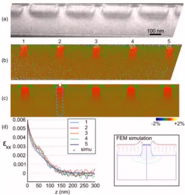
300⫻800 nm2兲 but this can be enlarged by modifying the projector lenses system. Figure2共a兲shows the widest obser-vation that we have been able to obtain on the SACTEM with an acceleration voltage of 200 kV. The limit is deter-mined by the size of the CCD camera, and in particular, the Nyquist frequency limit for the holographic fringes. The ex-posure time is 10 s and the fringes period is only 2.5 pixels. Although contrast and precision are reduced, the field of view has been doubled 共1.6 m兲. The overlap itself is un-changed as this depends on the biprism voltage.
It is now possible to map the deformation field in five different transistor channels in just one acquisition, which ensures that the reference is exactly the same for each tran-sistor and allows a statistical analysis of the measured strain distributions. Figure 2共d兲 shows the profiles taken in each separate channel from the gate to the substrate. The width of integration corresponds to the length of the channels: 65 nm. There is an excellent agreement between all of the measured profiles, with each curve following exactly the same trend, including the slight deviation about 65 nm from the gate. Indeed, the standard deviation between the profiles is only 0.02%, which expresses the precision of our measurements. The maximum value, just below the gate, is 0.58%⫾0.02%, which suggests that the reduced sampling has not introduced a significant systematic error.
To estimate the accuracy of the method we have realized a finite element method 共FEM兲 model based on linear elasticity theory.26,16 Initially, we performed full three-dimensional simulations 共150 nm thick兲 with free surfaces and a geometry that mimics that one revealed by TEM bright-field images 关Fig.1共a兲兴. The results show no signifi-cant thin foil relaxation, mainly due to the large thickness and the specific geometry of the specimen. To simplify sub-sequent calculations, we therefore turned to a 2D plane-strain
FIG. 2. 共Color online兲 Dark-field hologram analysis of transistor array: 共a兲 dark-field hologram with the 共220兲 diffracted beam, 共b兲 corresponding xx strain map relative to Si substrate,共c兲 FEM simulation, and 共d兲 strain pro-files from five different channels from gate oxide to substrate. Maximum strain under the gate is 0.58%⫾0.02%.
model which is sufficient for our purposes. The surfaces of the TEM lamella are considered to be rigid and only the upper surface 共in the z direction兲, near the oxide, is free.
The two following subdomains are considered: one with Si properties 共bulk elastic constants and lattice parameter兲 and another with Si1−yCyproperties. The nominal value of y
is 1% but not all carbon atoms are incorporated on substitu-tional sites, and thus contribute to the modification of the lattice parameter.27,28 From -Raman experiments on uni-form layers we can estimate that only between 75%共Ref.29兲
and 90%共Ref.22兲 of carbon atoms are involved in the strain
process. Figure 2共c兲shows the results from the best fitting FEM model with y = 0.75%, a mesh step of 4 nm and iden-tical color scale to the experimental results in Figs.2共b兲and
1共d兲. We have confirmed the value of 0.75% for the substi-tutional carbon by analyzing the lattice parameter in the Si:C layer in the z direction with a 共002兲 dark-field hologram.
The simulated profile ofxxfollows closely the trend of
the experimental results 关Fig. 2共d兲兴. The standard deviation
between the average of the experimental profiles and the simulation is only 0.01%, although a systematic difference of 0.04% occurs nearer the gate. This is reflected in the maxi-mum reached by the simulation, 0.53%, compared with the experiment value of 0.58%. The underestimation of the strain by the model is probably due to the difficulty of reproducing exactly the same boundary conditions, such as the effect of the top oxide, or the gate and the surface platinum layer.
We have demonstrated that dark-field holography is a valuable tool for the study of strained-silicon n-MOSFETs where strains tend to be relatively small and highly localized. Strain can be measured to extremely high precision共2.10−4兲 and mapped across large field of view 共300 nm by 1.6 m兲 with good spatial resolution共4 nm兲. By studying five neigh-boring transistors, information of a statistical nature can be obtained. The Si channels have a longitudinal strain xx
which is maximal near the gate oxide at a value of 0.58%⫾0.02% before decreasing progressively toward the substrate. The FEM modeling shows that the results are con-sistent with a substitutional carbon content in the recessed sources and drains of 0.75% of the total carbon concentra-tion.
This work was supported by the European Commission through the ESTEEM project 共Enabling Science and Tech-nology for European Electron Microscopy, Grant No. IP3: 0260019兲, the French Government 共MINEFI兲 through the NANO2012 initiative 共project IMASTRAIN兲, and by the French National Agency共ANR兲 in the frame of its program in Nanosciences and Nanotechnologies 共HD STRAIN Project No. ANR-08-NANO-0 32兲. Peter Verheyen and Roger Loo共IMEC兲 are gratefully acknowledged for supply-ing the device material.
1The International Technology Roadmap for Semiconductors, Edition 2007,
Process Integration, Devices & Structures.
2M. L. Lee, E. A. Fitzgerald, M. T. Bulsara, M. T. Currie, and A.
Lochtefeld,J. Appl. Phys. 97, 011101共2005兲. 3E. A. Fitzgerald,Mater. Sci. Eng., B 124, 8共2005兲.
4S. E. Thompson, G. Sun, Y. S. Choi, and T. Nishida,IEEE Trans. Electron Devices 53, 1010共2006兲.
5D. A. Antoniadis, I. Aberg, C. Ni Chleirigh, O. M. Nayfeh, A.
Khaki-firooz, and J. L. Hoyt, IBM J. Res. Dev. 50, 363共2006兲.
6S. Ito, H. Namba, T. Hirata, K. Ando, S. Koyama, N. Ikezawa, T. Suzuki,
T. Saitoh, and T. Horiuchi,Microelectron. Reliab. 42, 201共2002兲. 7C. H. Chen, T. L. Lee, T. H. Hou, C. L. Chen, C. C. Chen, J. W. Hsu, K.
L. Cheng, Y. H. Chiu, H. J. Tao, Y. Jin, C. H. Diaz, S. C. Chen, and M. S. Liang, Dig. Tech. Pap. - Symp. VLSI Technol. 2004, 56.
8G. Eneman, P. Verheyen, R. Rooyackers, F. Nouri, L. Washington, R.
Schreutelkamp, V. Moroz, L. Smith, A. De Keersgieter, M. Jurczak, and K. De Meyer,IEEE Trans. Electron Devices, 53, 1647共2006兲.
9Y. Liu, O. Gluschenkov, J. Li, A Madan, A. Ozcan, B. Kim, T. Dyer, A.
Chakravarti, K. Chan, C. Lavoie, I. Popova, T. Pinto, N. Rovedo, Z. Luo, R. Loesing, W. Henson, and K. Rim, Dig. Tech. Pap. - Symp. VLSI Technol. 2007, 44.
10C. J. Chui, K. W. Ang, N. Balasubramanian, M. F. Li, G. S. Samudra, and
Y. C. Yeo,IEEE Trans. Electron Devices 54, 249共2007兲.
11K. W. Ang, J. Lin, C. H. Tung, N. Balasubramanian, G. Samudra, and Y.
C. Yeo, Dig. Tech. Pap. - Symp. VLSI Technol. 2007, 42.
12J. Huang, M. J. Kim, P. R. Chidambaram, R. B. Irwin, P. J. Jones, J. W.
Weijtmans, E. M. Koontz, Y. G. Wang, S. Tang, and R. Wise,Appl. Phys. Lett. 89, 063114共2006兲.
13P. Zhang, A. A. Istratov, E. R. Weber, C. Kisielowski, H. F. He, C. Nelson,
and J. C. H. Spence,Appl. Phys. Lett. 89, 161907共2006兲.
14W. Zhao, G. Duscher, G. Rozgonyi, M. A. Zikry, S. Chopra, and M. C.
Ozturk,Appl. Phys. Lett. 90, 191907共2007兲.
15K. Usada, Y. Numata, T. Irisawa, N. Hirashita, and S. Takegi,Mater. Sci. Eng., B 124-125, 143共2005兲.
16F. Hüe, M. J. Hÿtch, F. Houdellier, J. M. Hartmann, H. Bender, and A.
Claverie,Phys. Rev. Lett. 100, 156602共2008兲.
17M. J. Hÿtch, F. Houdellier, F. Hüe, and E. Snoeck,Nature共London兲 453,
1086共2008兲.
18M. J. Hÿtch, F. Houdellier, F. Hüe, and E. Snoeck, Patent Application No.
FR 07 06711共pending兲.
19K. J. Hanszen,J. Phys. D 19, 373共1986兲.
20P. Favia, D. Klenov, G. Eneman, P. Verheyen, M. Bauer, D. Weeks, S. G.
Thomas, and H. Bender, in Strain Study in Transistors with SiC and SiGe
Source and Drain by STEM Nano Beam Diffraction, edited by S. Richter
and A. Schwedt 共EMC, Springer Berlin Heidelberg, 2009兲 Vol. 2, pp. 15–16.
21H. Itokawa, N. Yasutake, N. Kusunoki, S. Okamoto, N. Aoki, and I.
Mi-zushima,Appl. Surf. Sci. 254, 6135共2008兲.
22P. Verheyen, V. Machkaoutsan, M. Bauer, D. Weeks, C. Kerner, F.
Clem-ente, H. Bender, D. Shamiryan, R. Loo, T. Hoffmann, P. Absil, S. Biese-mans, and S. G. Thomas,IEEE Electron Device Lett. 29, 1206共2008兲. 23E. Snoeck, P. Hartel, H. Mueller, M. Haider and P. C. Tiemeijer,
Proceed-ings of the International Microscopic Conference 共IMC 16, Sapporo,
2006兲 Vol. 2, p. 730.
24F. Houdellier, M. J. Hÿtch, F. Hüe, and E. Snoeck, Advances in Imaging and Electron Physics, edited by P. W. Hawkes 共Elsevier, Amsterdam,
2008兲, Vol. 153, Chap. 6, pp. 1–36.
25M. J. Hÿtch, E. Snoeck, and R. Kilaas,Ultramicroscopy 74, 131共1998兲. 26Y. C. Yeo and J. S. Sun,Appl. Phys. Lett. 86, 023103共2005兲.
27J. M. Hartmann, T. Ernst, V. Loup, F. Ducroquet, G. Rolland, D. Lafond,
P. Holliger, F. Laugier, M. N. Séméria, and S. Deleonibus,J. Appl. Phys. 92, 2368共2002兲.
28V. Le Thanh, C. Calmes, Y. Zheng, and D. Bouchier,Appl. Phys. Lett. 80,
43共2002兲.
29N. Cherkashin, M. J. Hÿtch, F. Houdellier, F. Hüe, V. Paillard, A. Claverie,
A. Gouyé, O. Kermarrec, D. Rouchon, M. Burdin, and P. Holliger,Appl. Phys. Lett. 94, 141910共2009兲.