A 35.6TOPS/W/mm$^2$ 3-Stage Pipelined Computational SRAM with Adjustable Form Factor for Highly Data-Centric Applications
Texte intégral
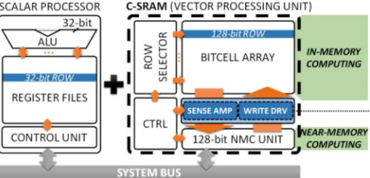
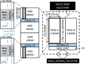
Figure
Documents relatifs
Energy efficiency, behavior, awareness, evaluation, energy savings accounting, office buildings, white certificates, energy management
Market volume is also necessary to be evaluated by national market regulators and central banks in order to have current information on global tendency of their
Detection rate: We showed that the detection of a real movement was easier than discrete and continuous motor imageries but we could discuss about the weakness of the
La restauration de la connectivité paysagère en Lorraine offre l’opportunité d’étudier comment la végétation de forêt ancienne recolonise les fragments
Parmi les 108 cas de notre étude, le taux de la glycémie à jeun était disponible pour 96 patients et élevé chez 21 patients (22%), ce résultat est comparable à l’étude faite
NSP antibodies in cattle, pigs or sheep following administration of a double dose 20.. or a
L’archive ouverte pluridisciplinaire HAL, est destinée au dépôt et à la diffusion de documents scientifiques de niveau recherche, publiés ou non, émanant des
compound was to carry out in silico a ligand‐based rational design, also known as “indirect” drug design. In brief, starting from the structure
