HAL Id: hal-03022348
https://hal.archives-ouvertes.fr/hal-03022348
Submitted on 24 Nov 2020HAL is a multi-disciplinary open access archive for the deposit and dissemination of sci-entific research documents, whether they are pub-lished or not. The documents may come from teaching and research institutions in France or abroad, or from public or private research centers.
L’archive ouverte pluridisciplinaire HAL, est destinée au dépôt et à la diffusion de documents scientifiques de niveau recherche, publiés ou non, émanant des établissements d’enseignement et de recherche français ou étrangers, des laboratoires publics ou privés.
Local heat generated by a Foccussed He+ ion beam
Makoto Sakurai, Shoko Nagano, Christian Joachim
To cite this version:
Makoto Sakurai, Shoko Nagano, Christian Joachim. Local heat generated by a Foccussed He+ ion beam. Nanotechnology, Institute of Physics, 2020. �hal-03022348�
1
Local heat generated by a focused He
+ion beam
Makoto Sakurai1, Shoko Nagano2 and Christian Joachim3,1
1
International Center for Materials Nanoarchitectonics (WPI-MANA), National Institute for Material Sciences (NIMS), 1-1 Namiki, Tsukuba, Ibaraki 305-0044, Japan
2
Research Center for Advanced Measurement and Characterization, National Institute for Material Sciences (NIMS), 1-1 Namiki, Tsukuba, Ibaraki 305-0044, Japan
3Centre d’Elaboration de Matériaux et d’Études Structurales (CEMES), Centre National de
la Recherche Scientifique (CNRS), 29 Rue J. Marvig, BP 4347, 31055 Toulouse Cedex, France
Email: [email protected]
Abstract
Focused He+ beam with a beam diameter lower than 1 nm is heating up the targeted surface for He+ dose larger than 1×10²⁰ ions/cm2. The temperature can reach locally 1000 °C resulting in surface decompositions or chemical reactions. This temperature was measured by fabricating gold nano-disk down to 20 nm in diameter and 10 nm in thickness on mica and sapphire surfaces. The melting and vaporization of those nano-disks were used to determine this temperature according to the known gold nanoclusters melting temperature variations as a function of their volume. This local heat production is very negative for precise He+ nanolithography resist processes but advantageous without a resist to directly nano-sculpture a nanomaterial when a very thermally conductive support like sapphire is selected.
Keywords: Focused He ion beam, scanning helium microscope, heat generation, size-dependent melting temperature, gold nano-disk
2
Introduction
Focused beams of charged particles used for example in nanolithography (e-beam, Ga+ beam) are generating heat locally when reaching the resist and wafer material interfaces [1]. This is also the case of the recent focused He+ beam nanolithography processes where the patterns are generally deformed by the lateral melting of the resist [2] and as a consequence by the local deformation of the surface of the wafer supporting those patterns [3,4]. This is clearly a problem for HIM fabricating nanoelectronics circuits [5], ultrathin nano-disk or nano-gears beyond the known e-beam nanolithography limits [6]. To measure locally this local heat dissipation, we have used here gold metallic nanodisks playing the role of a local nanothermometer [7]. This “all or nothing nanothermometer” effect was inspired from the 75 nm in diameter nanothermometer filled up with Ga carbon nanotube [7]. We take benefit of the fact that at small dimensions, the melting temperature of a metallic nanocluster depends on its effective diameter [8-10], an effect known since the seminal work of M. Takagi [11]. It offers a unique opportunity to evaluate the local temperature of a gold nanodisk as a function of the He+ dose focused on it. The resulting local heat production may be enough to trigger surface chemical decompositions or surface reactions leading to surface deformations often larger than a few nanometres in corrugation [3,5].
Results and discussion
We have thermally prepared 10 nm, 20 nm and 100 nm in thickness Au(111) gold layers on fresh cleaved mica and ultra-flat c(0001) sapphire (Shinkosha Co., Kanagawa, Japan) substrates. An Orion Plus helium ion microscope (HIM) (Zeiss, Peabody, USA) operating at an acceleration voltage of 30 keV was used to irradiate focussed He+ beams at the surface of those substrates. HIM images were recorded with doses of 0.7 - 7×10¹⁰ ions/cm2 to reduce the anticipated irradiation damages. The spatial resolution of the He+ beam was 0.35 – 0.5 nm. The irradiation was achieved by using the internal Orion patterning software to raster the focussed beam with a 1 nm pixel spacing. A constant beam current of 0.4 pA was used for all the experiments, taking care of the stability of the He+ emitting trimer on the tip. The dwell time per pixel was adjusted to achieve the required dose. The dose for a complete local etching depended on the Au thickness and on the supporting material. In our experiments, we have used mica (thermal conductivity κ = 44 W/cm·K) and sapphire (κ = 4.2 W/cm·K) substrates to observe heat generation and transfer to the supporting surface during the
3
irradiation of focussed He+ beam onto the gold nanodisk with a κ = 319 W/cm·K gold film thermal conductivity.
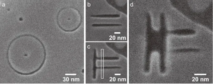
As presented in figure 1a, 100 nm thick layer Au(111) nanodisks can be directly sculptured on the sapphire surface down to 20 nm in diameter using an He+ focussed beam irradiation [10] with a dose reaching 1×10¹⁹ ions/cm2 including the central mark. Depending on the supporting surface, a reduction of the sculptured pattern down to 10 nm renders locally the gold layer unstable under He+ irradiations. As presented in Fig. 1b, c, d, a simple sculpturing experiment on a gold/mica surface demonstrates that this effect is mainly due to a local heating of the supporting surface by the He+ focused beam. During the etched lines (Fig. 1b, c), the gold layer was not destabilized by those successive irradiations. As soon as the 4th irradiation was performed to sculpture a single 10 nm × 20 nm gold nano-island on mica, the awaited nano-island was vaporized laterally by this last irradiation step (Fig. 1d) indicating a drastic increasing of the local temperature of the mica surface.
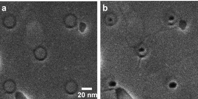
To study systematically this effect, we have fabricated a series of Au(111) nanodisks on mica and sapphire substrates with different diameters from 5 nm up to 50 nm (see for example Fig. 2a for a series of identical 20 nm in diameter gold nanodisks on a sapphire surface). Then, the He+ beam was focussed at the centre of each nanodisk while increasing step by step the irradiation time as indicated in Fig. 2b. As a result, the centre of the nanodisk can be either pierced as for example in Fig. 1a on sapphire or vaporized similar to the effect which was presented in Fig. 1b, c, d on mica.
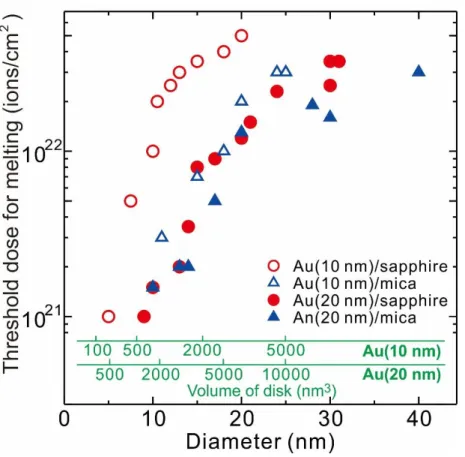
As presented in Fig. 3, the threshold for melting a gold nanodisk depended on the irradiation time and on the thickness of the gold layer. The difference of melting threshold between mica and sapphire is small for an Au(111) layer with a thickness of 20 nm even if the sapphire thermal conductivity is about 10 times larger than the one of mica. This small melting threshold difference is due to the same adsorption energy of the gold atoms on sapphire and mica surfaces because of the similarity of surface atomic scale structure between the two materials. More interesting is the fact that a nanodisk made from a thin gold layer is able to sustain a larger irradiation dose than a one made with a thick layer. This effect partially comes from the small stopping power of He+ beams at a surface [12,13], leading to diffuse elastically through a thin gold layer without transferring its energy to this gold layer via inelastic scattering processes. The effect is also partially originating from the diffusion of the thermal energy caused by the He+ impact on the thin gold layer to the substrate. The latter is effective for thin layers as well as a substrate with large thermal conductivity. For thicker
4
gold layers, the inelastic effect occurs within the layer. The nanodisk melts and evaporates at larger He+ doses.
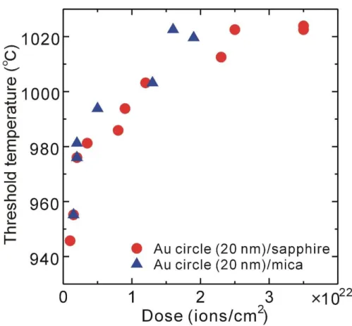
The Fig. 4 curves can serve to estimate the local temperature of a 20 nm in thickness gold layer on the mica and sapphire surfaces under He+ focused beam irradiations. For this purpose, we have used the well know melting temperature variation formula as a function of the volume of the material [11,14]:
Tm(V) = TB (1 – V
-1/3
) (1)
where is a parameter characteristics of the material and of its shape (layered, spherical, and ovoidal). Notice that (1) is normally applied to metallic nanoparticles where V -1/3 is simply
proportional to the nanoparticle diameter. For gold, bulk melting temperature TB is 1085 ℃. In
our case, V is simply the volume of the initial disk diameter before its melting and vaporization with a 20 nm layer thickness. In (1), we have taken = 1.387 nm to approach the experimental variation of the gold melting temperature as a function of V [14]. Following the Fig. 3 data, Tm(V) can be plotted as a function of the He+ focused irradiation dose. This
leads to the Fig. 4 curves demonstrating that under He+ irradiation, the local temperature can be as high as 1020 ℃.
This local temperature increase has 2 consequences:
(1) when a material is irradiated by a focussed He+ beam, a pervasive perception that the surface is not impacted by the irradiation is not valid. Certainly, a focussed He+ beam is not back scattered in the material due to low stopping power [15],and the behaviour is different from the backscattering of the focussed electrons very active in an e-beam nanolithography process. The heat locally generated at the material-surface interface by a focussed He+ beam can deform this surface by initiating local chemical reaction well before the creation of the deep in the material He bubbles [16]. For a sapphire material, this heat production can also desorb oxygen and create random conductive aluminium paths which we have detected through local surface conductance measurements.
(2) This local heat production can also chemically transform the nanomaterial deposited on the supporting surface. This can be the case of He+ sensible resist now used in He+ nanolithography or in the re-stabilization of a nanomaterial which was supposed to be etched by the He+ beam. This last example was observed in measuring room temperature electronic transport localization effects through a graphene monolayer [3].The first randomization of the graphene surface atomic scale structure by the He+ beam irradiation was very conclusive. But
5
step by step, the localization effect disappears demonstrating that the previously randomly damaged graphene areas were reforming their initial honeycomb atomic structure. We have originally interpreted this phenomenon as a lateral diffusion of the graphene carbon atoms reforming its graphene hexagonal lattice [3]. This diffusion is only possible because a local heating effect occurring on the sapphire surface. This is exactly what we have confirmed here using ultra small metal nanodisk as nanothermometers.
Conclusion
Focused He+ beam is hardly heating up locally a surface when scattered. He+ ions can continue deep in the material their trajectory underneath the surface. But inelastic scattering effects also occur at the material-surface interface leading to a local temperature increase up to 1020 °C. On the supporting surface, the resulting local heat production is large enough to trigger surface chemical decompositions or reactions. It explains the large surface corrugation increase while for example performing local atomic scale atom extractions [3,5]. It can have a negative effect for He+ nanolithography processes. But this is also an advantage (when mastered) to sculpture directly a nanostructure without a resist deposited on the surface using also a very thermally conductive material like sapphire.
Declaration of Competing Interest
The authors declare that they have no known competing financial interests or personal relationships that could have appeared to influence the work reported in this paper.
Acknowledgements
This work was supported in part by the World Premier International Center (WPI) Initiative on Nanoarchitectonics (MANA), MEXT, Japan and in part by the European FET-Open project MEMO (Grant N°766864). We thank Dr. H. Oosato for preparation of Au thin layers.
References
[1] Dayen J F, Mahmood A, Golubev D S, Roch-Jeune I, Salles P and Dujardin E 2008 Small 4 716-720
[2] rdo a R, Mailly D, Rezaev R O, Smirnova E I, Schmidt O G, Fomin V M, Zeitler U, illam n I, Suderow H and Teresa J D 2019 Nano Lett. 19 8597-8604
6
[3] Verveniotis E, Okawa Y, Nakaharai S, Ogawa S, Nakayama T, Aono M and Joachim C 2019 Jpn J. Appl. Phys. 58 055007
[4] Nakaharai S, Iijima T, Ogawa S, Suzuki S, Li S L, Tsukagoshi K, Sato S and Yokoyama N 2013 ACS Nano 7 5694-5700
[5] Naitou Y., Iijima T. and Ogawa S. 2015 Appl. Phys. Lett. 106, 033103
[6] Yang J., Deng J., Troadec C., Ondarcuhu T. and Joachim C. 2014 Nanotechnology 25, 465305
[7] Gao Y and Bando Y 2002 Nature 415 599
[8] Lai S L, Guo J Y, Petrova V, Ramanath G and Allen1 L H 1996 Phys. Rev. Lett. 77 99-102
[9] Buffat Ph and Borel J-P 1976 Phys. Rev. A13 2287-2298
[10] Allen G L, Bayles R A, Gile W W and Jesser W A 1986 Thin Solid Films 144 297-308
[11] Takagi M 1954 J. Phys. Soc. Jpn 9 359-363
[12] Scipioni L, Ferranti D, Smentkowski V S and Potyrailo R A 2010 J. Vac. Sci. Technol.
B28 C6P18-C6P23
[13] Stanford M G, Lewis B B, Mahady K, Fowlkes J D and Rack P D 2017 J. Vac. Sci.
Technol. B35 030802
[14] Schmid, G. and Corain, B. 2003 Eur. J. Inorg. Chem. 3081-3098
[15] Petrov Y V and Vyvenko O F 2016 Helium Ion Microscopy (eds. Hlawacek G and Gölzhäuser A.) Springer Chap. 5
7
Figure 1. (a) An HIM image of two Au(111) nano circles nanofabricated using the same
focused He+ beam with an 1×10¹⁹ ions/cm2 irradiation dose on a 100 nm thick Au(111) layer deposited on an atomically flat sapphire sample surface. A little central irradiation was also performed in the center of each nanodisk to prepare the Fig. 2 experiment. (b)-(d) HIM images of an Au(111) nano rectangle step by step nanofabrication process near the edge of a 100 nm thick Au(111) layer on mica using a line by line scan of a focused He+ beam with a dose of 6×10¹⁸ ions/cm2. Step b and c, the central gold layer is stable. After the b step, a new line by line irradiation with a dose of 6×10¹⁸ ions/cm2 was performed as indicated by the white transparent rectangle on this figure. In the HIM image just after this second step, the central gold nano rectangle vaporized without scanning on it.
8
Figure 2. (a) The HIM beam sculpturing of 5 metallic nanodisks in an 20 nm thick Au(111)
layer deposited on a sapphire surface using a 1×10¹⁹ ions/cm2 He+ beam irradiation dose. (b) Each nanodisk was He+ beam irradiated at its center with a different dose to determine its melting threshold which can be observed by a progressive disappearance of the external black circle and a large extension of the central pierced hole: top left: 1s (1×10²¹ ions/cm2), top right: 5s (5×10²¹ ions/cm2), center: 10s (1×10²² ions/cm2), bottom left: 20s (2×10²² ions/cm2), and bottom right: 30s irradiation time (3.0×10²² ions/cm2). Here, the nanodisks have the same 20 nm diameter. The disk diameter was also systematically varied from 5 nm to 40 nm to record the Fig. 3 curves.
9
Figure 3. (Color online) Variation of the melting (or vaporization) threshold dose as a
function of the nanodisk diameter sculptured on Au(111) layer with a thickness of 20 nm and 10 nm, thermally deposited on a mica and a sapphire surface.
10
Figure 4. (Color online) Variation of the local surface temperature measured using the change
of the melting temperature of metallic nanodisk of different diameter for a mica and sapphire surface