HAL Id: tel-01612546
https://tel.archives-ouvertes.fr/tel-01612546
Submitted on 7 Oct 2017HAL is a multi-disciplinary open access archive for the deposit and dissemination of sci-entific research documents, whether they are pub-lished or not. The documents may come from
L’archive ouverte pluridisciplinaire HAL, est destinée au dépôt et à la diffusion de documents scientifiques de niveau recherche, publiés ou non, émanant des établissements d’enseignement et de
Electrical characterization and technological
optimization of Conductive Bridge RAM CBRAM
devices to improve performance, speed and reliability
Marinela Barci
To cite this version:
Marinela Barci. Electrical characterization and technological optimization of Conductive Bridge RAM CBRAM devices to improve performance, speed and reliability. Micro and nanotechnolo-gies/Microelectronics. Université Grenoble Alpes, 2016. English. �NNT : 2016GREAT022�. �tel-01612546�
THÈSE
Pour obtenir le grade de
DOCTEUR DE LA COMMUNAUTÉ UNIVERSITÉ
GRENOBLE ALPES
Spécialité : Nanoélectronique et nanotechnologies
Arrêté ministériel : 7 août 2006
Présentée par
Marinela BARCI
Thèse dirigée par Dr. Barbara DE SALVO et codirigée par Dr. Gabriel MOLAS
préparée au sein du Laboratoire CEA- Leti, Grenoble et Altis Semiconductor, Corbeil -Essonnes
dans l'École Doctorale d’Électronique, Électrotechnique, Automatique et Traitement du Signal
Caractérisation électrique et
optimisation technologique des
mémoires résistives Conductive Bridge
Memory (CBRAM) afin d’optimiser la
performance, la vitesse et la fiabilité
Thèse soutenue publiquement le 6 Avril 2016,devant le jury composé de :
M Gérard GHIBAUDO
Directeur de Recherche CNRS (IMEP-LAHC), Président
M Abdelkader SOUIFI
Professeur, Institut National des Sciences Appliquées (INSA) de Lyon, Rapporteur
M Amara AMARA
Professeur, Institut Supérieur d’Électronique de Paris (ISEP), Rapporteur
M Damien DELERUYELLE
Maître de Conférence, IM2NP, Université d'Aix-Marseille, Examinateur
Mme Barbara DE SALVO
Directeur de Recherche, Cea-Leti, Grenoble, Directrice de thèse
M Pascal LOUIS
Ingénieur, Altis Semiconductor, Corbeil-Essonnes, Responsable Industriel
M Gabriel MOLAS
Ingénieur chercheur, Cea-Leti, Grenoble, Co-encadrant de thèse, Membre invité
M Daniel BERTRAND
Abstract
Flash technology is approaching its scaling limits, so the demand for novel memory technologies is increasing. Promising replacing candidates are the emerging non volatile technologies such as Conductive Bridge Memory (CBRAM), Oxide based Resistive RAM (OXRAM), Magnetic Random Access Memory (MRAM) and Phase Change Memory (PCRAM). In particular, CBRAM is based on a simple Metal-Insulator-Metal (MIM) structure and presents several advantages compared to the other technologies. CBRAM is non volatile, i.e. it keeps the information when the power is off, it is scalable down to 10nm technology node, it can be easily integrated into the Back-End-of-Line (BEOL), finally, it has high operation speed at low voltages and low cost per bit. Nevertheless, demands for the industrialization of CBRAM are very stringent and issues related to device reliability are still to be faced. In this thesis we analyze two generations of CBRAM technology, each one addressing a specific application market. The first part of the PhD is dedicated to the electrical study of Cu-based/GdOx structures, which present the advantages of a very stable data retention and resistance to soldering reflow and also good endurance behavior. This CBRAM family addresses mainly the high temperature applications as automotive. To fulfill the specification requirements, doping of metal-oxide and bilayers are integrated to decrease the forming voltage and increase the programming window. Better endurance performance is also achieved. The second part is dedicated to a new CBRAM technology, with a simple MIM structure. In this case, the device shows fast operation speed of 20ns at low voltages of 2V, combined with satisfying endurance and data retention. This technology seems to be compatible with the growing Internet of Things (IOT) market. In summary, during the PhD research, the main objective was to study the reliability of the embedded CBRAM devices in terms of forming, endurance and data retention. Some methodologies were developed and the electrical set-up was modified and adapted to specific measurements. Physical models were developed to explain and better fit the experimental results. Based on the obtained results, we demonstrate that the CBRAM technology is highly promising for future NVM applications.
Résumé
La technologie Flash arrive à ses limites de miniaturisation. Ainsi, la nécessité de nouvelles technologies mémoire augmente. Les candidats au remplacement des mé-moires Flash sont les technologies non volatiles émergentes comme les mémé-moires à pont conducteur (CBRAM), résistives à base d’oxyde (RRAM), mémoires magné-tiques (MRAM) et mémoires à changement de phase (PCRAM). En particulier, les mémoires CBRAM sont basées sur structure simple métal-isolant- métal (MIM) et présentent plusieurs avantages par rapport aux autres technologies. La CBRAM est non volatile, à savoir qu’elle garde l’information lorsque l’alimentation est coupée, ses dimensions peuvent être réduites jusqu’au nœud 10 nm, elle peut facilement être intégrée dans le Back-End d’une intégration CMOS, enfin, elle a une vitesse de fonctionnement élevée à basse tension et un faible coût de fabrication. Néanmoins, les spécifications pour l’industrialisation des CBRAM sont très strictes. Dans cette thèse, nous analysons deux générations de technologie CBRAM, chacune adressant un marché d’application spécifique. La premiére partie de la thèse est consacrée à l’étude électrique des structures à base de cuivre et de GdOx, qui présentent comme
avantages une conservation des données trés stable et une bonne résistance lors de la soudure des puces, et un bon comportement de léndurance. Cette technologie adresse principalement les applications à haute température telle que l’automobile. Pour ré-pondre aux spécifications, un oxyde métallique dopé ainsi que des bicouches sont intégrés pour réduire la tension de formation de la mémoire et augmenter la fenêtre de programmation. Les performances en endurance sont améliorées. La deuxiéme partie est dédiée à une nouvelle technologie de CBRAM, avec un empilement de type MIM. Dans ce cas, nous avons démontré des temps de commutation trés ra-pides de 20 ns à basses tensions (2 V), combinés avec une endurance satisfaisante et une bonne rétention des données. Cette technologie semble être compatible avec les applications Internet des objets (IOT). En résumé, au cours de ce doctorat, lóbjectif principal était d’étudier la fiabilité des dispositifs embarqués CBRAM en termes d’écriture des données, endurance et la conservation de l’information. Une méthodologie de test spécifique a été développée, afin d’évaluer les performances des technologies étudiées. Des modèles physiques ont été mis au point pour expli-quer et analyser les résultats expérimentaux. Sur la base des résultats obtenus, nous démontrons que la technologie de CBRAM est trés prometteuse pour les futures applications de mémoires non volatiles.
Contents
1 Introduction 3
1.1 Memory Market study and trends . . . 3
1.2 State-of-Art: Mature and Emerging NV memories . . . 5
1.2.1 FLASH technology . . . 5
1.2.2 RRAM technology . . . 8
1.2.3 Other emerging NV memories . . . 12
1.2.4 Summary of emerging NVM . . . 14
1.3 RRAM single device and demonstrators performances . . . 17
1.4 Motivation of this work . . . 20
2 Overview of the studied CBRAM technology 21 2.1 CBRAM configuration . . . 22
2.2 Electrical characterization methodology . . . 22
2.2.1 Forming in QS and Pulsed Mode . . . 23
2.2.2 SET and RESET Operation . . . 24
2.2.3 Short pulse measurements . . . 25
2.2.4 High temperature data retention . . . 26
2.2.5 Cycling endurance . . . 27
2.2.6 Pre-forming . . . 28
2.3 Modeling . . . 29
2.3.1 2D numerical model . . . 29
3 CBRAM - Study of Data retention 31 3.1 State-of-Art: Data retention study of CBRAM technology . . . 31
3.2 Sample description . . . 33
3.3 Methodology . . . 34
3.4 Numerical model . . . 35
3.5 Results and discussion . . . 36
3.5.1 LRS . . . 36
3.5.2 HRS . . . 38
3.5.3 Temperature activation . . . 39
3.6 Conclusions . . . 41
4 Bilayer devices to improve memory performances 43 4.1 State of Art: Electrical performances of bilayer metal-oxide RRAM . 43 4.1.1 Gd2O3/(10%) Cu-MoOx, Yoon et al., Microelec. Eng. 2009 . . 43
4.1.2 HfOx/AlOx RRAM, Yu et al., VLSI-TSA 2011 . . . 44
4.1.3 Ni/ HfOx/ AlOy/p+-Si, Tran et al., EDL 2011 . . . 46
4.1.4 Pt/ZrOx /HfOx/TiN, Jung et al., APL 2010 . . . 48
4.1.5 Pt /CuxO/ SiO2/Pt, Yi et al., NVMTS 2008 . . . 50
4.1.6 TiN/TiOx/HfOx/TiN, Chen et al., IEDM 2009 . . . 52
4.1.7 Mono and Bilayer CBRAM technology studied in this work . . 54
4.2 Results and discussions . . . 54
4.2.1 Quasi - static measurements . . . 55
4.2.2 Pulsed - mode measurements . . . 55
4.2.3 Data retention . . . 57
4.2.4 Endurance . . . 59
4.2.5 Modeling and discussion . . . 62
4.3 Conclusions . . . 64
5 Generation 3 metal-oxide CBRAM technology compatible for low power applications 67 5.1 State of Art: Advantages of the new technology to be compatible with IOT applications . . . 67
5.2 Technological details, set-up and methodology . . . 68
5.3 Experimental Results . . . 68
5.3.1 Quasi - static measurements . . . 68
5.3.2 Short-pulse measurements . . . 70
5.3.3 Pulsed - mode measurements . . . 73
5.3.4 Endurance . . . 75
5.3.5 Data retention . . . 80
5.4 Conclusions . . . 81
6 General Conclusions and Perspectives 84 A Résumé en français 87 A.1 Mémoires non-volatiles émergentes . . . 87
A.1.1 Technologies de mémoire non volatile émergentes . . . 87
A.1.2 Démonstrateur et leurs performances . . . 90
A.1.3 Motivation . . . 90
A.2 CBRAM étude de la conservation des données . . . 92
A.3 Dispositifs CBRAM bicouches pour améliorer les performances de la mémoire . . . 101 A.3.1 Conclusion . . . 110 A.4 Génération 3 CBRAM pour des applications a basse puissance . . . . 111 A.4.1 Conclusion . . . 119 A.5 Conclusions General . . . 121 A.5.1 Perspectives . . . 123
B Author’s publications 124
Manuscript Outline
The manuscript is organized in 6 chapters.In Chapter 1, we introduce the context and motivation of the research done during these three years of the PhD. A description of the memory market and RRAM/CBRAM State-of-the-Art are given in details.
In chapter 2, an overview of the studied CBRAM technology is given, the inte-gration flow and the main applications are shown. The methodology to characterize the reliability of our structures is given for both 1T1R and miniarrays configu-ration, including in forming, SET/RESET opeconfigu-ration, screening of the parameters during SET and RESET operations, endurance measurements, thermal stability and soldering-reflow. A new set-up was realized to measure cycling endurance for short-pulse measurements. A new idea was proposed to improve uniformity and facilitate "forming" process. Numerical models were developed to explain the experimental results.
Chapter 3 focuses on the thermal stability of CBRAM technology. It is shown that the electrical measurements are in good agreements with the physical model, able to explain the retention behavior. "Smart" RESET operation was proposed to improve retention and Arrhenius plot was used to extract the temperature at 10 years retention is guaranteed. A region showing stable LRS and HRS retention behavior is demonstrated for different programming currents. Low power consumption is shown for 30 µA. Measurements were performed up to 300 °C.
In Chapter 4, we propose a bilayer metal-oxide/Al2O3CBRAM device that shows
improvement in HRS and cycling endurance up to 1 × 10⁵cycles. The electrical
results are shown for both mono and bilayer devices. A 2D numerical model is developed to explain endurance failure behavior. A "smart" endurance test was proposed to reach 1 × 10⁶cycles cycles increasing applied voltages during SET and
RESET progressively until the initial target resistance is reached.
In chapter 5, we introduce a new generation of CBRAM technology, with the advantage of using simple materials (easier to integrate) and low power consumption. Reliability tests were performed for our devices regarding forming, cycling endurance using pulses of minimum 20 ns up to 1 µs and data retention up to 200 °C.
In chapter 6, a summary of the results we obtained during the thesis is presented. Finally, we also provide some prospects on the future work to be done in order to improve our technology and make it suitable for NV market demands.
Acknowledgements
This PhD thesis was prepared in collaboration between the Universite Grenoble Alpes, CEA LETI and Altis Semiconductor. First, I would like to express my special appreciation and thanks to my thesis director Dr. Barbara De Salvo. I would like to thank her for encouraging my research and for allowing me to grow as a research scientist. Then, I would like to thank my supervisors Dr. Gabriel Molas and Dr. Elisa Vianello for supporting and helping me during my thesis. I want to thank all the LCM team: Luca Perniola, Eric Jalaguier, Gabriele Navarro, Veronique Sousa, Alain Persico, Christelle Charpin, Sophie Bernasconi, Carine Ja-han, Remi Coquand, Etienne Nowak, Laurent Grenouillet, Catherine Carabasse, Jean-Francois Nodin. It was a pleasure to be part of your team and to work with you. I thank Anne Roule, Mathieu Bernard, Philippe Blaise, Stephane Becu, Alain Lopez, Jacques Cluzel, Denis Blachier, Carlo Cagli, Giovanni Romano and all the people from LCTE and LICL laboratories for their support. I thank my colleagues from Altis Semiconductor: my manager Pascal Louis, Daniel Bertrand, Michel Sar-langue, Brahim Belgacem, Mehdi Kanoun, Jacques Liebault, Pascal Verrier, Faiz Dahmani and Emilie Jansingh and all the others who I did not mention. Thank you for your fruitful discussions, lunches, coffee breaks and for more that you gave me the opportunity to have an experience in industry during my PhD. I thank all the PhD students, interns and postdocs who shared with me great moments during the last three years: Daniele, Thanasis, Manan, Boubacar, Quentin, Thomas, Gabriele, Giorgio, Therese, Jeremy, Florian, Yann, Sebastien, Amine, Julien, Issam, Sarra, Heimanu, Remi, Luca, Niccolo, Thilo, Julia, Mourad, Mouhamad, Giuseppe, Cecile, Adam, Daeseok, Luc, Martin, Aurore, Fabien, Loic, Romain, Vincent, Mathilde, Corentin, Anouar, Mathias, Patricia, Alexandre. I am sorry if I have forgotten someone. I would like to thank Sabine and Brigitte for their help and availability during these three years. I am grateful to Prof. Gerard Ghibaudo, Prof. Abdelkader Soufi, Prof. Amara Amara and Prof. Damien Deleruyelle for accepting to review this thesis and for their useful comments, remarks and questions during my PhD defense. I thank my family for being the greatest support in my life, for teaching me that you need to work hard, believe in yourself and never give up if you want to fulfill your dreams. Last, but not least I want to thank all my professors from the primary school to PhD, for their knowledge, help and support.
Chapter 1
Introduction
In this chapter we will give a general view of memories. In a first part we will discuss about the memory market study and the trends for applications such as stand-alone, embedded and Storage Class Memory. Among the mature and emerging non volatile memories, we want to identify the role of CBRAM in the memory market study. Then a section on the State-of-the-Art of memories is given in details, starting from Flash and the evolution of other emerging memories such as CBRAM, OxRAM, PCRAM and MRAM. Some comparison between CBRAM and other memories is given, identifying both the advantages and issues related to each technology. The latest publications are mentioned, explaining each product and its specifications. The last part will be dedicated to the motivation of this work.
1.1
Memory Market study and trends
Memory can be either volatile and non-volatile memoriy (NVM).Depending on their applications, NVM are classified into stand-alone, embedded and storage class mem-ory SCM. Classic volatile memories consist in SRAM and DRAM and they are the most common used in the nowadays applications dominating the market for stand-alone applications around 35.6 B$ as shown in Fig.A.1b and around 60 % for the mobile micro processors (MPU) and micro-controllers (MCU) applications as shown in Fig.A.1a. Somehow they do not keep the information after the power is turned off. For this reason novel NV memories are having more and more attention. The data in Fig.A.1a shows that they occupy 1.3 B$ of the stand-alone market and 27 % of automotive and micro-controllers market cost. NAND and DRAM stand-alone memories dominate the memory market, representing about 90 % of overall memory sales. Among the emerging NVM we can mention phase change memory PCM, mag-netic random access memory MRAM, ferroelectric RAM FeRAM, resistive switch memory (also called ReRAM, CBRAM, OxRAM), polymeric-based memory, molec-ular memory etc as shown in Fig.1.4. These memories should overcome the scaling
1 – Introduction
(a)
(b)
Figure 1.1. (b)Memory market chart for stand-alone applications. (a) Memory market chart for embedded applications [1].
issues which effect Flash memory, the most mature NV technology with a presence in the market of 28.7 B$. Predictions show that by 2020, emerging NVM market will grow up to 7 B$ by 2020 with Enterprise Storgae as the largest market due to fast adoption of RRAM and STT-MRAM as represented in Fig.A.3. Wearable is the second growing market because of the strong demand for low power. SCM is evolving as a cathegory of memory targetting to fill the gap between RAM and SSD in terms of short latency and high density. It combines the benefits of solid-state memory, such as high performance and robustness, with the archival capabilities and low cost of conventional hard-disk magnetic storage. Such a device requires a nonvolatile memory (NVM) technology that could be manufactured at a very low cost per bit. The main parameters determing its evolution are: latency, endurance, volatility and cost [1].
1 – Introduction
The schematics shown in Fig.A.2 highlights the applications in industry and trans-portation up to mass storage memory applications. IOT is catching more and more attention and the demand for smart and wearable electronics is increasing. With its advantages as low power and fast switching speed, CBRAM stands as one of the promising future memory. Many research centers and companies are investing in NVM memory field in the level of start-up companies as Adesto, Crossbar, Cro-cus Technology; Integrated device manufacturers as Samsung, Toshiba or foundries as TSMC, GlobalFoundrais. Their business is encouraged by data centers, social network and ebusiness players as Facebook, Google and eBay.
Figure 1.2. Applications of new emerging RRAM technologies [1].
1.2
State-of-Art: Mature and Emerging NV
mem-ories
1.2.1
FLASH technology
Flash is considered a mature NV memory technology and it is already available in the market in current memory applications. It is divided into 2 groups NAND and NOR Flash architectures. NOR are suitable for code storage, while NAND are more used for data storage. These memories are based in Si-CMOS technology, having an additional floating gate between the MOSFET channel and the controlling gate as shown in Fig.1.6. Since it is isolated by insulating oxide, electrons are trapped in this area and the transistor is set in the logical "0" state. So a higher voltage is needed to be applied in the controlling gate to make the channel conductive, which
1 – Introduction
Figure 1.3. Main contributors in NV Memories development [1].
Figure 1.4. Memory classification including volatile and non volatile, both mature and emerging technologies [3].
increases the threshold voltage of the transistor(Vt1 higher than Vt2) and puts it in
1 – Introduction
Figure 1.5. Emergin NVM market trend by applications from 2014-2020 [1].
should be in the intermediate state. If the transistor conducts, the floating gate is not charged, so a logical "1" is stored in the gate. Otherwise if the transistor does not conduct at this applied voltage, the floating gate is charged and a logical "0" is stored. Experimentally this is proved by measuring the current passing through the transistor at this intermediate voltage, which allows single bit or multibit cell device depending on the charge stored in the floating gate. NAND flash memory is also used in hard disks or optical media (e.g. CD, DVD). One example is the microSD card which has an area of about 1.5 cm2, with a thickness of less than 1 mm and
offers presently up to 16 GB of storage capacity at the same time [3].
Figure 1.6. Schematic of a Flash cell. Single bit or multibit storage is possible depending on the charge stored in the floating gate.
NAND has become the cheapest and densiest device in the semiconductor indus-try. 64 Gb and 128 Gb monolithic MLC NAND are already in production at 16 and
1 – Introduction
(a) (b)
Figure 1.7. (a) Vertical NAND cell integration presented by Samsung. (b) Vertical NAND specifications [4].
15nm half-pitch [4]. But planar Flash is approaching its limits due to scaling. Now the focus has moved to the integration of vertical NAND (Fig. 1.7a and Fig. 1.7b). Its main advantages with compared to planar NAND are density, cost and threshold variability is reduced for vertical NAND related to program and RTN with a great advantage for multilevel storage, [5].
1.2.2
RRAM technology
Conductive Bridge RAM CBRAM
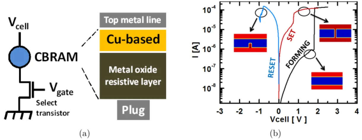
In this chapter we will focus on the ReRAM. These memories consist in a MIM (Metal-Insulator-Metal) structure. The top electrode (the anode) is made of an electrochemically metal as Ag or Cu as shown in Fig.1.8. The solid electrolyte can be a chalcogenide as GeS2, GeSe or a metal oxide as HfOx, GdOx,Ta2O5 etc.
The bottom electrode or the cathode is made of an inert metal such as W, Pt. When a positive bias is applied between top and bottom electrode, the state of the device is switched between HRS (High resistive state) and LRS (Low resistive state) and viceversa if the bias polarity is reversed. The schematic of CBRAM switching mechanism is shown in Fig.1.9.
This behavior is called bipolar. To use the same terminology we will refer to LRS as the ON-state of the device and HRS to the OFF-state. The resistance change is due to electro-chemical formation and dissolution of conductive filaments. When a positive voltage is applied on the top electrode, metal atoms are oxidized and dissolve into the solid electrolyte. Under the electric field these metal cations immigrate towards the bottom electrode where they are reduced and deposited. This process
1 – Introduction
Figure 1.8. Schematic behavior of a CBRAM cell integrated into 1T1R configuration.
continues and a conductive filament (CF) is formed between the cathode and anode, shunting the resistance from HRS to LRS. When a negative voltage is applied, the CF dissolves and resistance is switched back to HRS. Current - induced Joule heating may also contribute to the filament rupture. The device can switch between HRS and LRS many times, since electro-chemical reaction does not cause big damage to the CBRAM device. For memories with metal sulfides as solid electrolyte, mobile ions as Ag+ already exist in the electrolyte. But for other metal oxides, the mobile ions are external and usually a "forming" process is performed to drive these ions into these materials, before stable resistive switching can be achieved. This forming value is higher than the other subsequent Write operations named SET.
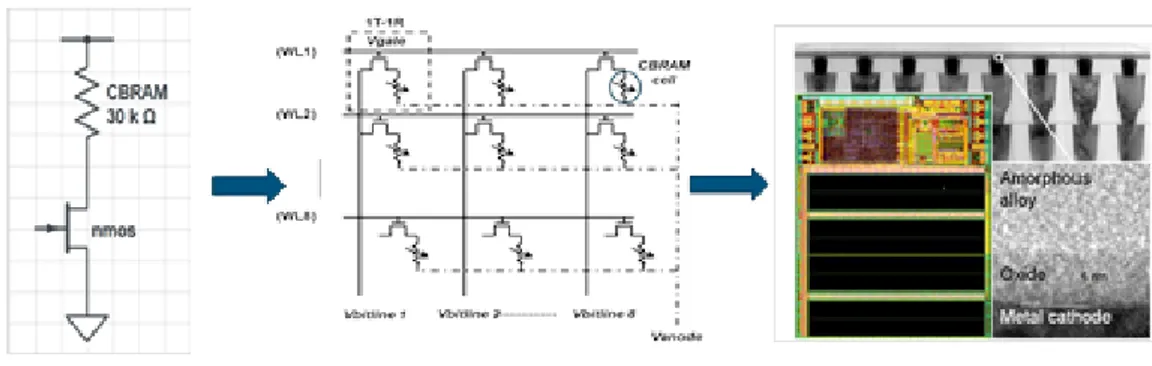
CBRAM technology is considered as a promising technology due to its many advantages, among them most interesting are: CBRAM is non volatile, it keeps the information when the power is off, it is scalable down to 10 nm technology node [6], [7]. It can be integrated into the BEOL. It has high operation speed at low voltages. Even if a lot of research has been conducted from different research laboratories and companies, some issues related to device reliability and controllability still have to be addressed [3]. Some demonstrators (Fig.1.10a) of 2 Mbit first generation CBRAM integrated in 90 nm technology are shown from Altis Semiconductor and 1 Mbit array second generation CBRAM integrated into 130 nm technology presented by Adesto are already available in the market [8]. In Fig. 1.10b a 4 Mb product is presented by Sony [9]. A 16 Gb Cu-ReRAM integrated in 27 nm technology node is shown in Fig. 1.11a and Fig. 1.11b by Sony-Micron [10], [11] and [12].
Oxide-based Resistive RAM
They are also named OxRAM or Valence Change Memory (VCM). RRAM are com-posed of a MIM structure, normally a thin insulator film, more in general metal-oxide
1 – Introduction
Figure 1.9. Current-Voltage behavior of a CBRAM cell.
(a) (b)
Figure 1.10. (a) 1 Mbit array CBRAM presented by Adesto at IEDM 2013 [8]. (b) 4 Mb CBRAM array and its specification are presenteed by Sony at ISSCC 2011 [9].
(TiO2,HfOx) is sandwiched between 2 metal electrodes made of Pt. Other
metal-oxides as TiOx, AlOx, WOx and SrTiOx have also been exploited and show bipolar behavior. The basic operation lies in a redox mechanism. When a voltage is applied on the top electrode (Fig.1.12), oxygen vacancies and oxygen anions are generated into the insulating layer. The O2-flows towards the positively biased electrode and
oxidizes TiO2 into Ti2O5, which increases the barrier height, increasing the
struc-ture’s resistance. If the voltage polarity is inversed, oxygen vacancies flow towards the negatively biased electrode, reducing the TiO2 insulating layer, so reducing its
1 – Introduction
(a) (b)
Figure 1.11. (a) Cu-ReRAM cell integrated in 27 nm technology node. (b) 16 Gb die micrograph presented at ISSCC 2014 [12].
and convolutional neural network for pattern recognition applications. [13]–[15] OxRAM devices scale down to 8 nm with HfOx, they show 1 ns switching speed and energies of the order of pJ [16], [17]. Beside its excellent performances, one main issue with OxRAM devices remains variability and work is still needed to be done to fully understand its switching mechanisms in order to overcome this issue. Some demonstrators are shown in Fig 1.13a and its cell specifications (Fig. 1.13b) from Panasonic: 8 Mb TaOx ReRAM with write pulses of 8.2 ns [18] and [19] and Toshiba: 32 Gb ReRAM integrated in 24 nm CMOS technology.
Figure 1.12. Switching mechanism in binary metal-oxide RRAM.
1 – Introduction
(a) (b)
Figure 1.13. (a) OxRAM memory array and its bipolar diode JV characteristic was presented by Panasonic [18]. (b) Macrograph of the test chip description is given for 512 kbit 1T1R array [19].
[20]. The integration flow-chart of the cell composed of Ta2O5 and Ru bottom
electrode is shown in Fig. 1.14.
Figure 1.14. Switching mechanism in binary metal-oxide RRAM was presented by Renesas [20].
1.2.3
Other emerging NV memories
Transfer Torque STT-MRAMIn order to overcome the scalabilty and high cell writing current issues, Spin Transfer Torque Magentic RAM (STT-MRAM) proposes a magnetic tunnel junction (MTJ) structure composed of 2 ferromagnetic layers and a very thin MgO–based tunneling
barrier of less than 1nm. By applying a polarized electron current into the device, a change from parallel "1" to antiparallel "0" and viceversa occurs. The orentiation of the magnetization of the Free layer (FL) can be switched between two states and it is used to store information. The magnetization of the Reference layer (RL) is fixed. If the orientation of RL and FL are the same, the device is in Parallel (P) state,
1 – Introduction
(a) (b)
Figure 1.15. (a) Schematic view of a STT-MRAM cell. The MTJ is composed of a reference layer (RL), a tunnel barrier and a free layer (FL), both layers magnetized perpenticular to the plane of the junction [23]. (b) STT-MRAM electrical char-acteristics. Resistance versus applied magnetic field, showing bistable resistance states near zero-field associated with parallel (P) and antiparallel (AP) magne-tized bits. Resistance versus voltage, showing switching between AP and P states (positive bias) and vice versa (negative bias).
otherwise it is in Antiparallel (AP) state. The working principle of a STTRAM is based on two phenomena such as Tunneling Magento-Resistance (TMR) effect and the Spin Transfer Torque (STT) effect. TMR effect [21] is the ratio of resistance between parallel and antiparallel R. The resistance of the cell can be sensed in order to determine the magentic state of the FL, so the stored information can be retrived. While STT effect [22] is the effect which allows to switch the orientation of the magnetization of the FL. When electrons flow through the MTJ, a torque is exerted on the magnetization of FL, and if it is large enough, the magentic state of the FL can be switched and the information is written. If a positive bias is applied to the device, electrons with same spin orientation as RL magnetization will be transmitted by tunneling through the MTJ and will transfer their spin to the FL by STT. The MTJ will be in Parallel state. If a negative voltage is applied, the electrons are injected from the FL to the RL. In Fig. 1.15b is shown STT-MRAM electrical characteristics. Resistance versus applied magnetic field, showing bistable resistance states near zero-field associated with parallel (P) and antiparallel (AP) magnetized bits. Resistance versus voltage, showing switching between AP and P states (positive bias) and vice versa (negative bias). At the interface between the tunneling barrier and RL, electrons with the same orientation as RL will be transmitted through MTJ, while electrons with oposite orientation will be reflected back in the FL and switch its magnetization to AP state. Multilayers configuration is possible with stacked MTJs. STT-RAM have high endurance due to the fact that no magentic degradation mechanism is associated to the switching of the magnetization orientation [23]. 2 Mb STT-RAM with a MgO tunneling barrier using 0.2 µm2 technology process was
1 – Introduction
(a) (b)
Figure 1.16. (a) Schematic cross-section of a PCM cell. (b) IV characteristics of crystalline and amorphous phase of PCRAM materials [27].
Phase Change RAM PCRAM
The classical cell called "mushroom cell" Phase Change RAM (PCRAM) consists of memory storage or programmable region, most used is a chalcogenide GeSbTe ma-terial (Fig. 1.16a). When a voltage is applied in the top and bottom electrodes, it injects a heat pulse into the programming region of the chalcogenides phase change material [25], changing its state from amorphous high resistance state to polycrys-talline LRS. These high and low resistive states happen during "RESET" and "SET" operations. In PCRAM it is possible to switch the material between crystalline and amorphous many times. Crystallization is achieved by heating the material above its crystallization temperature (SET operation). Amorphization is achieved by melting the material in the liquid state and rapidly quenching it into disordered amorphous phase (RESET operation) as shown in Fig. 1.16b. One of the limita-tions to PCRAM technology is the relatively high RESET current [26]. PCRAM technology can enable Multi-Level-Cell MLC scaling.
It is implemented in both stand-alone and embedded applications. Some pro-totypes and demonstrators are shown from Samsung: 512 MB SLC memory chip integrated in 90 nm process with an area of 0.047 um2 and Numonyx Inc: 128 MB
integrated in 90 nm process [26].
1.2.4
Summary of emerging NVM
RRAM is interesting for eNVM applications compared to eFlash because it uses low power: 2-3 V instead of up to 20 V. It is low cost, about 20% less than eFlash and uses 3 extra masks layer instead of 10 used in eFlash. It is compatible with CMOS BEOL technology and it has 10-100 times faster write time. MCUs with eNVM tend
1 – Introduction
to be the workhorse for IOT, increasing the interest of eRRAM commercialization. Thermal stability is still an issue in order to replace eFlash. For the moment it was demonstrated stable retention behavior of 85 °C/10yrs in products and in research work around 110 °C/10yrs but this remains still lower than eFlash. RRAM is also compatible with standalone applications, but 3D RRAM is not ready to replace 3D NAND. RRAM remains a good option for Storage Class Memories (SCM) in order to close the gap between DRAM and NAND. SCM can be divided into 2 types: memory or storage mapped SCMs [5]. In order to be compatible for Memory SCM, the technology should replace a part of DRAM for power applications. Nowadays MRAM seems fitting better in terms of retention and cost but scalability below 20 nm is still an issue. To be compatible with storage SCM the main demands are low cost, NV and high density which emerging RRAM seems to compete. In order to reach low cost, cross-bar multilayer array of RRAM is exploited. Recent announcement was made by Intel-Micron with their 3D XPoint memory, which meets the requirements for storage SCM [28].
In addition to the device integration, a lot of research has been done regard-ing the selector device. Many options are used in the literature: as npn diodes, MSM (Mihnea et al., Sekar et al.), (Sandisk US patent), Metal-Insulator-Metal (MIM) structures (Panasonic), Ovonic Threshold Switch (OTS) presented by Kau et al., (Intel) and Mixed Ionic Electronic Conduction (MIEC) selector by G. Burr et al., (IBM). The main parameters evaluating a suitable selector are: selectivity (1 × 10¹⁰), endurance (1 × 10⁸), switching slope (< 5 mV/div), max current density
(> 5 × 10⁶A/cm2 and processing temperature (<300 °C) [29]. In Fig 1.17a the
inte-gration of FAST selector is shown and in Fig. 1.17b are shown its I-V characteristics at room temperature and 125 °C.
Thereafter, we summerize the reliability performances of OxRAM and CBRAM, according to [30]:
Forming
The stack considered for OxRAM is made of reactive Ti top electrode/amorphous ALD HfSIOx dielectric layer and TiN bottom electrode, while the stack for CBRAM consists in TE/Cu ion reservoir/electrolyte layer/TiN bottom electrode. Different sources for the formation of the filament are considered: In OxRAM there is a "soft-breakdown" of the dielectric while in CBRAM, the CF is formed due to electro-chemical ionization of Cu which is provided by external reservoir (TE). In CBRAM, forming voltage thus is lower than the breakdown voltage.
Endurance
Both technologies show feasible endurance up to 1 × 10⁶cycles as shown in Fig. 1.19
1 – Introduction
(a)
(b)
Figure 1.17. (a) Passive crossbar array integration of FAST selectors (single cell to 4Mb array). Images of the fabricated selectors. (b) I-V characteristics of the integrated selectors (isolated single cell, cells in 100Kb and 4Mb arrays) at 25 °C and I-V at 125 °C. [29].
(a) (b)
Figure 1.18. (a) Cell description and TEM image for the CBRAM cell. (b) Cell description and TEM image for the OxRAM cell [30].
driven by higher HRS.
Data retention
Both technologies were tested at high temperature of 150 °C/1hr at low operating current of 40 µA. The results are shown in Fig. 1.20. Improved stability is demon-strated for CBRAM structures.
1 – Introduction
Figure 1.19. Cycling behavior up to 1 × 10⁶cycles for both CBRAM and OxRAM technologies [30].
Figure 1.20. Retention behavior of the memory cell for CBRAM and OxRAM at 150 °C/1hr for low operating current of 40 µA [30].
ReRAM challenges
For both technologies there are some issues as variability and read/program noise as shown in Fig. 1.19, since ethe conducting filament is believed to approach a few atoms in size. High density applications require the cell to function with low programming noise, high variability and noise are significant product-level concern. OxRAM cells show 2x higher noise compared to CBRAM.
Beside the advantage of CBRAM, OxRAM uses simple materials (without the need of Cu integration) making it low cost and easier to be integrated in CMOS technology.
1.3
RRAM single device and demonstrators
per-formances
Memory devices have stringent requirements in order to be industrialized. The criteria are fixed from surveys of Emerging Research Device Work Group [3]. In terms of electrical performances the main characteristics consist in forming voltage and current, switching speed, power consumption, endurance cycling, data retention,
1 – Introduction
Figure 1.21. Normalized STD of single-cell LRS read current vs. median read current. OxRAM cells show 2x higher noise compared to CBRAM [30].
multibit capability, density, reproducibility and scaling. These parameters vary and one or another has priority depending in their applications: storage, memory, logic or neuromorphic as representing in Fig.1.22 as a demand to extend "CMOS Extension" and "Beyond CMOS" technologies. For memory applications the requirements and the data demostrated in the literature are promising and compatible [31]–[33].
In table A.1 are shown the performance parameters projected for scaled emerging research memory technologies STTRAM, CBRAM, PCM and OxRAM, the values are the one demonstrated in the literature and the one projected. These perfor-mances are positive and in the future they can replace Flash technology.
Figure 1.22. Device requirements corresponding to different mem-ory applications [31]–[33].
1 – Introduction
PCRAM MRAMSTT- CBRAM OxRAM Feature
Size F (nm)
Demonstrated 45 65 20 5
Projected 8 16 5 <5
Cell Area Demonstrated 4F2 20F2 4F2 4F2 Projected 4F2 8F2 4F2 4F2 Programming Voltage (V) Demonstrated 3 1.8 0.6 1 Projected <3 <1 <0.5 <1 Programming
Time (ns) DemonstratedProjected <50100 <135 <1<1 <1<1 Programming
Energy (J/bit) Demonstrated 6 · 10
−12 2.5 · 10−12 8 · 10−12 1 · 10−12
Projected 1 · 10−15 1.5 · 10−13 N.A. 1 · 10−16
Read
Voltage (V) DemonstratedProjected 1.2<1 1.8<1 <0.20.2 0.10.1 Retention
Time DemonstratedProjected >10yr>10yr >10yr>10yr >10yr>10yr >10yr>10yr Endurance
(nb. cycles) Demonstrated 10
9 1012 1010 1012
Projected 109 1015 1011 1012 Table 1.1. Comparison of the performance of the different emerging nonvolatile memory technologies according to the 2013 International Technology Roadmap for Semiconductor (ITRS), with projections for year 2026 [3].
1 – Introduction
1.4
Motivation of this work
Flash technology is approaching its scaling limits, so the demand for novel tech-nologies is increasing. Promising candidates are NV RRAM due to their simple structure, CMOS compatibility, low power, fast switching speed and scalability, low cost per bit. Some issues related to the understanding of the operating mecha-nisms and variability still need to be addressed. In order to address these issues and increase RRAM performances, material engineering for metallic electrodes [34] and the insulating layer are currently proposed, including the implementing of new methods for better quality material deposition. Correction algorithms are proposed to limit current overshoot, variability and increase the window margin. Memory select devices also need to be improved. A lot of research is focused on 3D crossbar integration of emerging technologies [35] with the advantage of higher density and they occupy less space. Market experts believe that the NVM will double by 2020, increasing its presence in both standalone and embedded applications. Also smart devices such as tablets and phones have been a driving force for increasing the de-mand of storage capacity. The main focus of this thesis is the CBRAM technology. An introduction of its State - of - the Art, operation principle and future applications was given in this Chapter. Recently, many companies and research laboratories pre-sented CBRAM with metal-oxides integrated as resistive layer. The devices show reliability improvements such as data retention, endurance and soldering reflow with respect to the previous technology which was based on chalcogenides as insulating layer [36], [8]. The main applications we targeted were high temperature and low power applications.
Chapter 2
Overview of the studied CBRAM
technology
A CBRAM device consists of a MIM structure. In the frame of this PhD, 2 main technologies have been implemented, using metal oxides as resistive layer. In the first case, we targeted high temperature embedded applications. The main issue for CBRAM to be compatible with these applications is thermal stability. In our devices, the top electrode is electro-chemically active, and is made of CuTeGe, the metal-oxide is composed of 5nm GdOx. The bottom electrode consists of an inert metal such as Ta or TaN plug of 200 nm of diameter. In order to have a lower forming voltage, GdOx has been doped with Hf up to 15% (measured by RBS). On the other hand in order to increase the memory window, thin layers (0.5 nm) of HfO2 and Al2O3 have been integrated together with GdOx. The evolution of
Altis CBRAM technology is shown in Fig. 2.1. First generation CBRAM consists in chalcogenides materials [36]–[38] as resistive layer, they show fast programming conditions, high window ratio and good endurance but do not stand the soldering reflow. In order to overcome this issue, CBRAM using metal-oxides were imple-mented. Typical metal-oxide materials are HfO2, Ta2O5, GdOx, Al2O3, ZrOx etc.
In our work we used Cu-alloy with GdOx oxide. In order to improve the CBRAM reliability, bottom interfaces as Hf, Ti were used. In GdOx layer doped with Hf and Al, the forming voltage was reduced to around 1V [39]. Better endurance and higher
ROF F were shown for bilayer devices as GdOx/Al2O3 and GdOx/HfO2. Beside the
good electrical performances with GdOx, in order to target low power applications, a new technology was integrated. The metal-oxide seems to be more robust than GdOx to Break-down, improving endurance cycling and keeping stable retention.
2 – Overview of the studied CBRAM technology
Figure 2.1. Schematic description of the CBRAM technologies developed in Altis.
2.1
CBRAM configuration
In 1 transistor 1 resistor (1T1R) configuration, the CBRAM cell is integrated into the BEOL of a 130 nm CMOS technology. By controlling the gate of the transistor, we can modulate the current passing through the device. In this work we also studied mini-arrays composed of 8 WL,8 BL and a common plate or anode is in common for all CBRAM devices. Each device itself is a 1T1R. So for the same area, we can integrate more devices. Starting from 1T1R structures, macros with densities of Mbit products are shown in literature as presented in Fig. 2.2 [8].
Figure 2.2. Integration of the CBRAM cell from 1T1R to Mbit products.
2.2
Electrical characterization methodology
The first type of measurement we performed to characterize the cell consists in reading the pristine resistance at low VAnode of 0.1V. This value indicates the initial
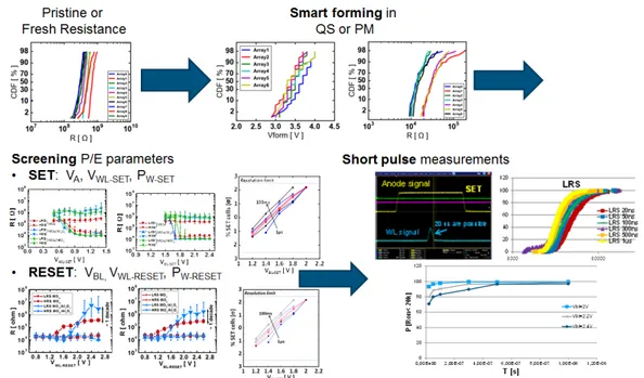
state of the metal-oxide: insulator or conductive. Also there are some criteria to be satisfied in order to be compatible with our products. The test is performed for several mini-arrays located in different positions of the 200 mm wafer. Then, a test sequence is performed in a CBRAM sample in order to evaluate the performances of the memory (Fig. 2.3).
2 – Overview of the studied CBRAM technology
Figure 2.3. Description of the methodology used to electrically character-ize CBRAM devices.
2.2.1
Forming in QS and Pulsed Mode
In order to study the operation principle of the CBRAM cell, measurements in Quasi-static mode are performed. Once we fix the operating current (Fig. 2.4a), we can study the characteristics of the CBRAM cell as shown in Fig. 2.4b. We apply a V in the anode of the device and we read the current passing through the cell through SMUs. As the V value is increased linearly there is a transition from HRS to LRS. This is due to the redox reaction of the anode and the diffusion of Cu-ions into the electrolyte. In presence of the high electric field, the Cu-ions are reduced in the inert electrode and they form a conductive filament. Normally the pristine R is high (> GΩ, so the current in the IV measurements before forming/switching are in the order of pA down to nA and the current signal cannot be distinguished from the background noise. VF orming corresponds to the first SET operation, and it
corresponds to the voltage value when switching to LRS occurs. Normally it is of the order of 2V to 3V in quasi-static (QS) mode. "Forming-free" devices would be preferred, compatible with our CMOS integrated in embedded 130nm technology. Moreover, the CMOS transistor integrated in a 130 nm technology can mantain
VF orming of 3.5V in pulsed mode. If the bias polarity wass reversed, the filament
dissolves, creating a gap between the bottom electrode and the remaining CF. In this case a transition from LRS to HRS occurs. The ROFF of the HRS is generally
lower than RP ristine; probabily due to the remaining part of the CF [6].
2 – Overview of the studied CBRAM technology
(a) (b)
Figure 2.4. (a) Current-Voltage behavior of the studied transistor. (b) IV charac-teristics of the CBRAM cell, for a given programming current.
overcome the variability from cell to cell and limit the energy brought to the system. Schematics illustrating of the progressive increase of VAnodein order to reach the LRS
target value, called "smart-forming" is given in Fig. 2.5.
Figure 2.5. Schematics illustrating the progressive increase of VAnode in order to
reach the LRS target value. This procedure is called "smart forming".
2.2.2
SET and RESET Operation
SET and RESET screening experiments aim at identifying the voltages to respec-tively SET and RESET the CBRAM, for a given pulse time. When SET operation is performed, the cell is switched back to LRS, currents of micro to mA are recorded. In fact the filament is recreated starting from the remaining CF. This operation can be repeated many times, making the device reliable for memory applications.
As we increase the applied V during RESET, ROF F increases up to a certain
value, then it starts to decrease for too elevated voltages. This is called "reverse SET", since the device should be in HRS, but in fact it comes back to the LRS, as represented in Fig. 2.6a. In the case of Generation 3 metal-oxide CBRAM, a more robust behavior was demonstrated and no breakdown is noticed up to VBL−RESET
of 3V. As ROF F is higher, the cell needs more V to be SET back to the LRS. In
2 – Overview of the studied CBRAM technology
(a) (b) (c)
Figure 2.6. (a) HRS as a function of the RESET V. (b) SET V as a function of the HRS. (c) LRS as a function of the programming current.
the cell is programmed in strong HRS, it needs more V to be put back to the LRS. The relation between the LRS and the programming current is shown in Fig. 2.6c during Forming and SET operation.
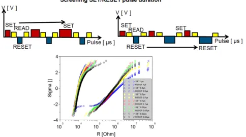
Screening SET/RESET parameters are done by parametric test in pulsed mode. From the graphs we can choose a trade-off between the programming conditions (VBL−SET, VBL−RESET, VW L−SET, VW L−RESET, PW during SET/RESET) for cycling
endurance and data retention depending on the targeted specifications. Typical pulse duration of 1 µs are used. First the cells are formed in Pulsed mode, using a "smart forming" sequence. There is variability in terms of VF orming from cell to
cell, so a progressive set starting from 2V (monolayer) or 2.5V (bilayer) up to 4V is performed in order to form the cells without stressing too much the stack. As V increases during RESET, ROF F also increases starting from LRS to HRS. While no
impact is noticed in LRS 2.7b. Starting from HRS, if we increase V during SET,
RON decreases abruptly up to 10th of 1 kΩ as the filament is formed 2.7a. The last
screening test is done to modulate pulse duration during SET and RESET operation as shown in Fig. 2.8. The R values are presented in median and percentiles (30%, 70%).
2.2.3
Short pulse measurements
The pulsed technique allows programming at different resistance values by applying pulses of different lengths or different pulse amplitudes. If we perform measure-ments in pulse mode, we need the cell to operate at pulse duration down to 20ns, which makes the instrumentation itself of high importance. In general short pulse measurements are performed by applying a time defined rectangular V pulse. This technique is used to SET/RESET and Read the CBRAM device. In order to target low power applications, we performed measurements in short pulses. The energy consumption is estimated by calculating the product of the applied voltage times programming current times the pulse duration.
2 – Overview of the studied CBRAM technology
(a) (b)
Figure 2.7. (a) Sequence and experimental results regarding screening parameters VAand VW Lduring SET operation. RESET conditions are fixed. (b) Sequence and
experimental results regarding screening parameters VBL and VW L during RESET
operation. RESET conditions are fixed.
Figure 2.8. Sequence and experimental results regarding screening pulse duration during SET and RESET operation.
2.2.4
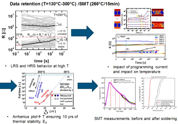
High temperature data retention
Retention measurements are performed at high temperatures in the oven, but read operation is done at room temperature (RT) and low V. It is important for the technology to maintain the information for 10 years. In Fig. 2.9 it is shown the schematics in order to program and erase the cells which will be used for data retention measurements. A schematic description of the methodology used to char-acterize data retention is given in Fig. 2.10. Normal operating T is 85 °C for chips in industry; we targeted HT applications so we performed measurements in high
2 – Overview of the studied CBRAM technology
Figure 2.9. Forming and Program/Erase sequence in order to perform data retention measurements.
T of 130 °C up to 250 °C. The parameter Nu, which is the slope of R(T) (resis-tance decay) or data loss factor is used quantify the data loss. To ensure 10 years, this parameter should be around 0.12-0.15. As ICC is increased better LRS
reten-tion stability is ensured, thus we performed LRS and HRS retenreten-tion characteristics starting from various initial resistance value. Soldering reflow measurements or SMT measurements are done at 260 °C for 15 to 20 min.
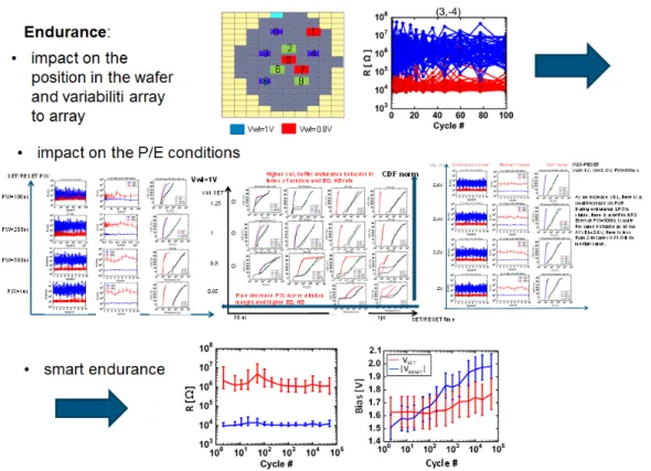
2.2.5
Cycling endurance
Depending on the application, endurance requirements vary; for DRAM replacement 1 × 10¹⁵cycles are required, while for embedded applications, the specifications vary
from 1 × 10³to 1 × 10⁶ Also the window ratio is important from the technological
point of view; a large window is preferred to have tolerance for designers. In Fig. 2.11 is shown the methodology used to characterize the cycling endurance of CBRAM.
Some correction algorithms are used in order to control this ratio from cycle to cycle. It may be time consuming so implementations with 2 to 3 pulse generators, applied in the VAnode, VW L, VBL during SET/RESET with short pulses are used.
During each operation, the resistance is checked and if it is not in the targeted range, programming voltage is increased during SET and RESET operation.
In order to identify the failure mechanism during cycling, we have defined the following parameters HB: it shows the % of the cells blocked in HRS during SET operation; BD: the % of cells which remain in LRS during HRS, HRS drif: resis-tance drift towards LRS as number of cycles is increased. Different programming conditions (VBL−SET, VBL−RESET, VW L−SET, VW L−RESET) are used in order to
eval-uate the endurance behavior and find the best operating conditions which offer the optimum cycling behavior. In fact, as we will discuss more in details in the next
2 – Overview of the studied CBRAM technology
Figure 2.10. Description of the methodology used to characterize electrically the retention performance at high temperature of CBRAM technology.
chapters, the programming conditions are important and determine the cycling be-havior and maximum number of cycles. Another parameter we used to quantify the endurance behavior is the yield, defined as the ratio between the number of cells, whose R is lower than a target RON value over the total number of tested cells. This
value is calculated for all the cycles and is expressed in percentage value.
2.2.6
Pre-forming
Beside the CBRAM traditional stack, we integrated a Ti thin layer in the bottom of the metal-oxide. We claim that if a "reverse" forming operation is applied prior to a normal forming operation, the electrical behavior of the CBRAM device is improved in terms of resistance and voltage distribution, which is very important in order to overcome the variability from cell to cell. In fact, "pre-forming" operation induces the creation of oxygen vacancies in the metal-oxide (Fig. 2.12). The presence of these defects make the R lowered compared to RP ristine, but still higher than the
RF orming. If a normal forming is applied afterwards, the conductive filament (CF)
is made of Cu-ions and the resistance values is of the order of the RF orming. After
2 – Overview of the studied CBRAM technology
Figure 2.11. Endurance behavior for monolayer and bilayer CBRAM devices up to 1 × 10⁵cycles
(which it is around some 1 GΩ), a reverse bias is applied in the anode (similar to a "RESET" operation), which we will call "pre-forming". It is shown that the pristine resistance value is modulated, being similar to ROF F (around some 100 kΩ). We
suppose that the presence of Ti induces oxygen vacancies in the oxide (and creates a TiOx interface!). After, a "normal" forming is applied, the oxygen vacancies facilitate the creation of the CF made of Cu-ions. The behavior is illustrated in Figs. 2.12, where pristine R, forming V and R distribution are shown for both cases.
2.3
Modeling
In order to explain and better understand the electrical results, we have developed some physical models as briefly explained above.
2.3.1
2D numerical model
A 2D numerical model developed in [41] was used to study the data retention be-havior of Cu/metal oxide CBRAM devices. We assume that the LRS resistance is controlled by the filament width, while the HRS resistance depends on the residual
2 – Overview of the studied CBRAM technology
Figure 2.12. Resistance and Voltage distribution schematics when a "pre-forming" operation is done [40].
filament width and height. The filament is composed of Cu atoms regularly dis-tributed in the resistive layer, each atom being treated independently. During bake, Cu atoms migrate following a Ficks law with a diffusion coefficient D. The local Cu concentration is locally computed in order to extract the local resistivity in every point of the electrolyte based on a semiconductor law. The cell resistance is then computed with a percolation model through a resistance network. It is thus possible to correlate the time evolution of RON and ROFF to the initial RON and ROFF values
(corresponding to different filament shapes) [42].
A TAT empirical model was used to calculate the amount of current and to explain the failure mechanisms during cycling for HRS CBRAM technology. The
ROF F decreasing during cycling can be explained by two mechanisms: defect
gen-eration and accumulation of Cu residual atoms (residual filament) in the resistive layer. In the case of the mono-layer CBRAM, we assume that the defects created in the metal oxide are at the origin of the endurance degradation. This model will be used in Chapter 4 to analyze the electrical results.
Chapter 3
CBRAM - Study of Data retention
In this chapter, we investigate the high temperature behavior of oxide-based con-ductive bridge memories. A methodology to optimize both high and low resistance states stability is presented. A numerical model is developed able to simulate the filament dissolution over time. This allows us to establish a clear correlation be-tween the filament morphology and the ON/OFF states stability. It is shown that the optimization of the memory programming conditions leads to a stable mem-ory window up to 250 °C. The CBRAM technology is highly promising as future non-volatile memories in general purpose micro-controllers (MCU) due to its low operating voltages, fast switching behavior, low integration cost and good CMOS compatibility. Nevertheless, in order to enable the technology, the high temperature stability must be addressed (in particular, to demonstrate data integrity after the peak temperature of reflow soldering). In this chapter, the role of SET and RESET conditions on retention behavior (data loss rate and activation energy) is clarified. We show that optimization of the programming conditions can drastically enlarge the high temperature memory retention. The experimental data are explained by means of numerical simulations, demonstrating a clear correlation between the fila-ment morphology/dissolution rate and the memory operating conditions.3.1
State-of-Art: Data retention study of CBRAM
technology
In this section, an overview of the retention study of RRAM will be given. Two main methods are usually adopted to accelerate data retention, either an accelera-tion by mean of an electric field [43], or a temperature activaaccelera-tion [44]. We mainly used for our studies the second method, where the device behavior is studied at different temperatures and by the means of Arrhenius plot, the temperature which ensures 10 years data retention is extracted. A summary of the literature review regarding data retention measurements and methodology is shown in Fig. 3.1. The
3 – CBRAM - Study of Data retention
Figure 3.1. Summary of the literature review on data retention regarding RRAM technology [45], [43], [41], [46], [44].
device parameters extracted from each work are: forming, SET/RESET voltage and current, endurance, thermal stability, physical model description, applications and improvement that they propose to improve retention degradation.
3 – CBRAM - Study of Data retention
Figure 3.2. Window ratio as a function of temperature for different ReRAM technologies. As the temperature is increased, the window margin is de-creased. By integrating a thin interface layer, the window is increased of almost 1 decade [8], [37], [39], [47]–[64].
T appears, with neglecting the impact of the baking time (normally more than 24 hours) and program/erase conditions. Each point corresponds to a given technology, considering CBRAM and RRAM in general [8], [37], [39], [47]–[64]. The graph explains the trade-off between the endurance and the thermal stability. As we can notice, as the temperature is increased, the window margin starts to decrease from 6 decades to almost 1 decade. If strong conditions are used to cycle the device (to achieve high programming window), less stability in temperature is noticed. In our case, we have integrated a thin insulating layer on top of the metal-oxide, in order to improve this margin of 1 decade and thus achieving stable retention properties at 250 °C, result which we will discuss in next chapter.
3.2
Sample description
The CBRAM technology studied in this work is composed of a Ta/GdOx/CuTeGe/TiN stack as shown in Fig. A.6a [65]. The memory cell consists in a resistor plus a tran-sistor used as selector (1T1R). Typical IV switching characteristics (Forming, SET and RESET) in quasi static modes are illustrated in Fig. A.6b. In the following, the experiments are performed in pulsed mode.
3 – CBRAM - Study of Data retention
(a) (b)
Figure 3.3. (a) CBRAM cell schematics for 1T1R structures. (b) Typical IV characteristics for CBRAM structure during Forming, SET and RESET operations.
3.3
Methodology
ON and OFF states retention characteristics were measured at various temperatures 130 °C-300 °C with several SET and RESET conditions, resulting in a large range of initial RON and ROFFvalues. The operating current provided by the selector
transis-tor controls the Low Resistance State (LRS), while the RESET conditions (voltage and pulse time) modulate the High Resistance State (HRS). Results reported in this paper correspond to the average over 100 cells. In Fig. 3.4 it is shown the flowchart in order to explain the "smart forming sequence" and the method to program the cell in LRS and HRS before the retention measurements. During "smart forming" we follow a read-write-read sequence, each time increasing progressively the voltage amplitude (from 2V to 3V) and compare with the target LRS (in our case this values is around 35 kW. Then 2.5 cycles are performed in cells which we want to program in LRS and 3 cycles in cells we want to program in HRS. After the devices are put in the oven at high temperature and we monitor the resistance value in logarithmic values of time up to 24 hours total measured time. The slopes of the LRS/HRS (time) retention characteristics (plotted in log-log scale) are extracted, leading to vON and vOFF parameters, respectively (Fig. A.8). The higher vON and |vOFF|, the
worse is the retention time. From the graph in Fig. A.8 we have extrapolated the parameter vON. This parameter describes the drift coefficient, it can qualitatively
express the loss of data retention as a function of time [42]. This is given by a power law as follows:
R = R0·(t/t0)v (3.1)
If we suppose a factor 10 of R
R0, the calculated drift coefficient after 1 × 10
5s
3 – CBRAM - Study of Data retention
Figure 3.4. Diagram explaining the methodology in order to study data re-tention of HRS and LRS. The programming sequence for "smart forming" and SET/RESET is shown on the right.
Figure 3.5. Measured LRS and HRS retention characteristics at 200° correspond-ing to a compliance current ISET= 100 µA. The parameter vON and vOFF are extracted for each case. They follow a power law.
is stable and below this value the retention behavior is unstable.
3.4
Numerical model
2D numerical simulations of the filament dissolution were performed to understand the experimental retention results. We assume that the LRS resistance is controlled by the filament width, while the HRS resistance depends on the residual filament width and height (Fig. A.7). The filament is composed of Cu atoms regularly distributed in the resistive layer, each atom being treated independently. The Cu
3 – CBRAM - Study of Data retention
Figure 3.6. LRS and HRS filament configuration used for retention simulations. Assuming a Ficks law for Cu diffusion during bake, local Cu concentration and cell resistance are computed with a percolation model.
concentration in the filament is adjusted in the x-axis in order to take into account the cylindrical shape of the filament: indeed, Cu concentration is higher in the center of the filament than close to the edges. This correction factor allows us to use 2D simulations, emulating a 3D filamentary behavior. During bake, Cu atoms migrate following a Ficks law with a diffusion coefficient D. The local Cu concentration is locally computed in order to extract the local resistivity in every point of the electrolyte based on a semiconductor law. The cell resistance is then computed with a percolation model through a resistance network. It is thus possible to correlate the time evolution of RON and ROFF to the initial RON and ROFF values (corresponding
to different filament shapes). The equations are reported above:
dx, y= sqrt(2 · D) · Rand(x, y) (3.2)
where
D= D0· exp(−EA/k · T) (3.3)
D is the diffusion coefficient, EA is the activation energy, D0 is the diffusivity
pre-factor, T is the temperature and ρ is the local resistance calculation, which follows a semiconductor law as shown above:
ρ= 1/σ = 1/(q · n · µ) (3.4)
3.5
Results and discussion
3.5.1
LRS
ON state retention curves are plotted in Fig. A.9 for various SET conditions, leading to an initial RON spread of more than 2 decades. The lower the initial resistance,
3 – CBRAM - Study of Data retention
Figure 3.7. Simulated and measured LRS characteristics at 130° for various initial RONcorresponding to compliance currents ISETranging from20 µA to 200 µA. High ISET corresponds to more stable LRS.
(a) (b)
Figure 3.8. (a) Simulated and measured LRS slopes (νON) extracted from reten-tion at 130° as a funcreten-tion of initial RON. A νON of 0.15 is assumed to ensure sufficiently large memory window after 10 years at 130°. Stable LRS are thus ob-served up to 100 k W. (b) Slope (νON) of LRS retention at 130° as a function of ROFF (before SET). No clear correlation between νON and ROFF appears.
the higher is the LRS stability. It can be noticed that the experimental curves are well reproduced by our numerical model. This result is confirmed by the decrease of
νON as the initial RON decreases (Fig. A.10a). In particular, the experimental data
and the model indicate that when RON< 1 × 10⁵, the filament is sufficiently thick
to be stable over time. For higher RON, the percolation becomes dominant and the
filament is more sensible to the Cu diffusion in the electrolyte during bake, leading to LRS instability. Finally, it appears that νON is completely uncorrelated to the
3 – CBRAM - Study of Data retention
(a) (b)
Figure 3.9. (b) νOFF parameter corresponding to the HRS and its dependency on the ROFF. (b) Slope of HRS (νOFF) as a function of ROFF at 130°. In the inset the retention characteristics with different initial ROFF are shown. Higher initial ROFF shows better retention behavior.
3.5.2
HRS
In Fig. A.11b, we plotted the measured and simulated HRS retention characteristics for various initial ROFFobtained by adjusting the RESET voltage (smart RESET). It
appears that a higher ROFF leads to a more stable HRS and a lower νOFF. We claim
that the height of the remaining filament in the electrolyte is reduced as the RESET conditions are strengthened. Thus, this leads to a larger gap between the remaining filament and the Cu-based top electrode, which prevents the reconstruction of a conductive path during bake. Then, we looked at the impact of RON value on the
HRS stability (Fig. A.10b). We show that, for a given initial ROFF, the HRS
stability is degraded when the memory has been previously SET to a low RON. To
confirm this trend, Fig. A.11a reports νOFF as a function of RON. Both experiments
and simulations exhibit a higher slope (corresponding for HRS to a stable behavior) as RON increases. This can be explained as follows: a lower RON leads to a thicker
remaining filament, yielding to more Cu atoms in the filament able to reconnect to the top electrode.
The retention characteristics at 130° with ISET = 80 µA are shown in Fig. 3.11.
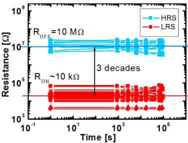
Almost 3 decades are maintain stable in median ROF F/RON value for 24 hours
retention time.
In Fig. A.12a it is represented the soldering reflow profile. The measurement is done at T = 260 °C for 15 min. The resistance distribution before and after soldering reflow is shown for LRS and HRS in Fig. A.12b. Both states show stable SMT behavior.
3 – CBRAM - Study of Data retention
Figure 3.10. Retention characteristics for same initial ROFFbut programmed with different LRS conditions.
Figure 3.11. Retention characteristics for LRS and HRS at 130° for ICC=80 µA.
3.5.3
Temperature activation
ON and OFF states retention characteristics were measured at various temperatures (85°- 300°) with ISET equal to 30 µA ,80 µA and 100 µA (Fig. A.14). The failure time
criterion was fixed to a critical variation ROFF/RON of a factor 2 (Arrhenius graphs
in Fig.A.15). Using a low programming current, LRS is controlling the lifetime while for high ISET HRS plays the critical role. Moreover, we can notice that the
maximum operating temperature for 10 years retention has drastically increased for higher SET currents (250° for ISET =80 µA ).
3 – CBRAM - Study of Data retention
(a) (b)
Figure 3.12. (a)Soldering reflow profile. The measurements were done at 260 °C for 15 min. (b) Cumulative distribution CDF of the LRS and HRS before and after soldering.
Figure 3.13. LRS and HRS retention characteristics at various temperatures (130° to 300°), with initial programming currents ISET equal to 80 µA or 100 µA.
3.5.4
Trade-off "retention vs. consumption"
Figure A.13 summarizes the νON and νOFF slopes extracted during retention
mea-surements at 130° as a function of the programming current ISET. A |νmax| value
![Figure 1.22. Device requirements corresponding to different mem- mem-ory applications [31]–[33].](https://thumb-eu.123doks.com/thumbv2/123doknet/12858464.368409/25.892.226.688.632.983/figure-device-requirements-corresponding-different-mem-mem-applications.webp)
![Figure 2.12. Resistance and Voltage distribution schematics when a "pre- "pre-forming" operation is done [40].](https://thumb-eu.123doks.com/thumbv2/123doknet/12858464.368409/37.892.152.743.162.603/figure-resistance-voltage-distribution-schematics-pre-forming-operation.webp)