HAL Id: hal-01139765
https://hal.archives-ouvertes.fr/hal-01139765
Submitted on 7 Apr 2015
HAL is a multi-disciplinary open access
archive for the deposit and dissemination of
sci-entific research documents, whether they are
pub-lished or not. The documents may come from
teaching and research institutions in France or
abroad, or from public or private research centers.
L’archive ouverte pluridisciplinaire HAL, est
destinée au dépôt et à la diffusion de documents
scientifiques de niveau recherche, publiés ou non,
émanant des établissements d’enseignement et de
recherche français ou étrangers, des laboratoires
publics ou privés.
Effect of annealing and Nd concentration on the
photoluminescence of Nd3+ ions coupled with silicon
nanoparticles
Olivier Debieu, David Bréard, Artur Podhorodecki, Grzegorz Zatryb, Jan
Misiewicz, Christophe Labbe, Julien Cardin, Fabrice Gourbilleau
To cite this version:
Olivier Debieu, David Bréard, Artur Podhorodecki, Grzegorz Zatryb, Jan Misiewicz, et al..
Ef-fect of annealing and Nd concentration on the photoluminescence of Nd3+ ions coupled with silicon
nanoparticles. Journal of Applied Physics, American Institute of Physics, 2010, 108 (11), pp.113114
1-8. �10.1063/1.3510521�. �hal-01139765�
Effect of annealing and Nd concentration on the photoluminescence of Nd 3 + ions
coupled with silicon nanoparticles
O. Debieu, D. Bréard, A. Podhorodecki, G. Zatryb, J. Misiewicz, C. Labbé, J. Cardin, and F. Gourbilleau
Citation: Journal of Applied Physics 108, 113114 (2010); doi: 10.1063/1.3510521 View online: http://dx.doi.org/10.1063/1.3510521
View Table of Contents: http://scitation.aip.org/content/aip/journal/jap/108/11?ver=pdfcov
Published by the AIP Publishing
Articles you may be interested in
Chemical bonding and defect states of LPCVD grown silicon-rich Si3N4 for quantum dot applications
J. Vac. Sci. Technol. A 32, 021507 (2014); 10.1116/1.4861338
Evidence of two sensitization processes of Nd3+ ions in Nd-doped SiOx films
J. Appl. Phys. 114, 033103 (2013); 10.1063/1.4813610
H-induced effects in luminescent silicon nanostructures obtained from plasma enhanced chemical vapor deposition grown Si y O 1 − y : H ( y > 1 ∕ 3 ) thin films annealed in ( Ar + 5 % H 2 )
J. Vac. Sci. Technol. A 24, 817 (2006); 10.1116/1.2177227
The evolution of microstructure and photoluminescence of SiCN films with annealing temperature
J. Appl. Phys. 99, 093503 (2006); 10.1063/1.2194208
The nanocluster coupling strength and its effect in excitation/de-excitation of Nd 3+ luminescence in Nd-doped silicon-rich silicon oxide
Appl. Phys. Lett. 83, 2778 (2003); 10.1063/1.1615837
Effect of annealing and Nd concentration on the photoluminescence of
Nd
3+ions coupled with silicon nanoparticles
O. Debieu,1,a兲D. Bréard,1A. Podhorodecki,2G. Zatryb,2J. Misiewicz,2C. Labbé,1 J. Cardin,1and F. Gourbilleau1
1
CIMAP, UMR CNRS/CEA/ENSICAEN/UCBN, Ensicaen 6 Bd Maréchal Juin, 14050 Caen Cedex 4, France
2Institute of Physics, Wroclaw University of Technology, Wybrzeze Wyspianskiego 27, 50-370 Wroclaw,
Poland
共Received 2 September 2010; accepted 30 September 2010; published online 9 December 2010兲 We report on the microstructure and photoluminescence共PL兲 properties of Nd-doped SiO2thin films
containing silicon nanoparticles 共Si-np兲 as a function of the annealing temperature and the Nd concentration. The thin films, which were grown on Si substrates by reactive magnetron co-sputtering, contain the same Si excess. Fourier transform infrared 共FTIR兲 spectra show that a phase separation occurs during the annealing due to the agglomeration of the Si excess resulting in the formation of Si-np. Besides, after annealing, the films exhibit PL from excitonic states confined in Si-np. We showed that the intensity of the PL of Nd3+ ions that occurs at ⬃0.92, 1.06, and 1.4 m is maximal at low Nd concentration and while well-passivated Si-np are formed. FTIR and x-ray measurements showed that the increase in the Nd incorporation has detrimental effects on the PL of Nd3+because of the formation of Nd
2O3nanocrystals and inherent disorder in the SiO2host
matrix. PL excitation measurements demonstrate that the PL of Nd3+ ions is nonresonant and
follows the excitation of Si-np giving new evidence of the energy transfer from Si-np toward the rare earth ions. © 2010 American Institute of Physics.关doi:10.1063/1.3510521兴
I. INTRODUCTION
Rare earth 共RE兲 ions, especially Er3+ and Nd3+ ions,
have attracted a considerable interest these last years because of their industrial applications. The former has been used for telecommunications because of the interesting radiative
4I
13/2→4I15/2 transition at 1.54 m that corresponds to the
absorption minimum of standard silica optical fibers.1 The latter has been highly used for solid-state laser applications due to the4F3/2→4I11/2transition at 1.06 m which presents
a high stimulated emission cross-section共⬇3⫻10−19 cm2兲.2
Furthermore, this transition occurs in a four-level medium where the lower level is well above the ground state which contrasts with the 1.54 m transition of Er that ends on the ground state in a three-level system. As a result, the achieve-ment of population inversion of Nd3+ ions can be achieved
with a lower threshold, thereby offering high laser gain effi-ciency like in the case of Nd:YAG crystal that is the most notable success of RE-based laser. One of the challenging fields of the last decades concerns silicon compatible light sources and amplifiers which are getting more and more at-tractive since they can be integrated to microelectronics devices.3 Unfortunately, whatever the host matrix, RE ions suffer from a low absorption cross-section as it has been reported in the case of Er3+ ions4,5and Nd3+ ions.2,6,7Since the discovery of the sensitizing effect of Si-nanoparticles 共Si-np兲 toward RE emission,8
RE-doped nanostructured Si-based films are promising for the achievement of future devices optically excited. Kenyon et al.9demonstrated that the pres-ence of Si-np in a SiO2host matrix resulted to an increase in the Er3+ photoluminescence共PL兲 by a factor of 100 and an
enhancement of the effective absorption cross section by four orders of magnitude.9,10 In such systems, RE ions benefit from the high absorption cross-section of Si-np by energy transfer. In contrast to Er3+ ions, such materials doped with Nd, have not been widely investigated and, accordingly, the energy transfer between Si-np and Nd3+ ions.11–18
Several authors have demonstrated that the energy transfer is more effective with small Si-np. Watanabe et al.11have shown that the increase in the Si-np average size from 2.7 to 3.8 nm results in a decrease in the PL intensity of Nd3+ions. In the
same way, Seo et al.12 have observed a decrease in the PL intensity of Nd3+ ions at 1.06 m with the increase in the
excess of Si, i.e., the increase in the Si-np average size. They concluded that only small Si-np which present excitonic states with a sufficient energy band-gap can excite the 4F3/2
level of Nd3+ ions. The effect of the Nd concentration in the optical properties of Nd-doped Si-np/SiO2 has been studied
by several groups.13,14MacDonald et al.13have changed the Nd content from 0.19 to 1.29 at.%. They have obtained a maximum of the PL intensity for a Nd concentration of ⬃0.29 at.%. Such a result underlines the problem of concen-tration quenching of RE ions in such Si-np/SiO2 systems
whose mechanism remains unknown.
In this paper, we describe the microstructure of Nd-doped silicon rich silicon oxide 共SRSO兲 thin layers synthe-sized by reactive magnetron sputtering by mean of Fourier transform infrared共FTIR兲 spectroscopy, and x-ray diffraction 共XRD兲. Their optical properties were investigated through PL, and total PL excitation measurements共TPLE兲. We exam-ine the influence of the evolution of the microstructure as a function of the annealing temperature and the Nd content on the PL properties of the films. We could describe the proper
a兲Electronic mail: olivier.debieu@ensicaen.fr.
JOURNAL OF APPLIED PHYSICS 108, 113114共2010兲
0021-8979/2010/108共11兲/113114/6/$30.00 108, 113114-1 © 2010 American Institute of Physics [This article is copyrighted as indicated in the article. Reuse of AIP content is subject to the terms at: http://scitation.aip.org/termsconditions. Downloaded to ] IP:
conditions to obtain efficient PL of Nd3+ but also its
limita-tions. The excitation energy dependence of Nd3+is compared
to the one of Si-np.
II. EXPERIMENT
In this work, amorphous hydrogenated Nd-doped SRSO thin films were deposited on p-type Si wafers by a reactive magnetron RF co-sputtering method that consists in sputter-ing simultaneously a pure SiO2 target topped with Nd2O3 chips. The Nd concentration is monitored by the surface ratio between the Nd2O3chips and the SiO2target. The sputtering gas is a mixture of argon and hydrogen; the latter enables to control the Si content of the deposited layers by reacting with oxide species in the plasma originating from the sput-tering of the target. More details on the reactive sputsput-tering method can be found elsewhere.18The films were grown at room temperature on Si substrates with a power density of 0.76 W/cm2. The samples were subsequently annealed at
high temperature ranging from 900 to 1100 ° C in a dry ni-trogen flow.
The infrared absorption properties were investigated by means of a Nicolet Nexus FTIR spectrometer at Brewster’s incidence. The XRD measurements were performed using a Philips Xpert NPD Pro diffractometer mounted with a point scintillation detector in the -2 configuration. The compo-sition of the deposited layers was determined by Rutherford backscattering spectrometry while the refractive index共given at 1.95 eV兲, as well as the film thickness, were determined trough ellipsometric spectroscopy analyses.
The PL measurements were performed at room tempera-ture using either a 266 nm semiconductor laser 共3 W/cm2兲 or an argon ion laser operating at 488 nm 共7.6 W/cm2兲 as excitation source. After 266 nm excitation, the UV-visible spectral range of the PL was detected by an HR4000 Ocean Optics spectrophotometer, while the near IR emission was collected by an InGaAs charge-coupled device camera after dispersion through a Jobin-Yvon TRIAX 550 monochro-mator. After 488 nm excitation, the PL was measured through a Jobin-Yvon THR 1000 monochromator mounted with a cooled Ge detector and a lock-in amplifier to record the near infrared spectra up to 1.5 m. The visible spectra were recorded with a fast photomultiplier共Hamamatsu兲 after dispersion of the PL with a Jobin-Yvon TRIAX 180 mono-chromator. The 266 and 488 nm excitation wavelengths are nonresonant lines with Nd3+ ions so that only an indirect
excitation of Nd trough the Si-np can occur.6,14,16
TPLE measurements were performed using a 450 W xe-non arc lamp as the excitation source, which was connected to a 0.18 m Jobin Yvon monochromator. The excitation power density was about 0.1 W/cm2 in the 210–480 nm
excitation range. A beam splitter redirected a part of the ex-citation light to a power-meter in order to monitor the wave-length dependence of the Xe lamp power. Thus, each ob-tained PL spectrum was corrected by the excitation power. The PL spectra were measured with the Ocean Optics HR4000 spectrometer.
III. RESULTS
In this study, we were interested in four Nd-doped SRSO thin films which have the same Si excess fixed to⬃7 at.%. After annealing at high temperature, Si-np are formed in the films in which the Nd content varied from 0.08 at.%, 0.27 at.%, 1.68 at.%, to 4.9 at.%共denoted as samples A, B, C, and D, respectively兲.
A. Microstructure
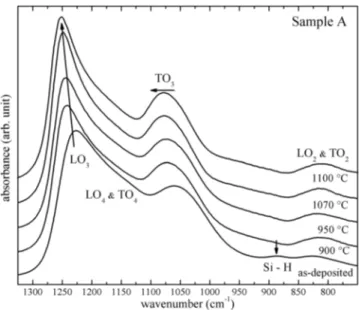
Figure 1 shows the evolution of the FTIR spectra of sample A as a function of the annealing temperature. The as-deposited sample shows a weak absorption band centered at⬃880 cm−1assigned to Si–H bonds. This band manifestly disappears after annealing because of the well known hydro-gen desorption process. Several bands characteristics of amorphous SiO2 are observed. The two prominent bands at 1220– 1250 cm−1and 1050– 1070 cm−1are assigned to
lon-gitudinal optical共LO3兲 and transverse optical 共TO3兲 phonons of Si–O bonds, respectively. The TO2, LO2, LO4, and TO4 vibration modes are also present at 810 cm−1, 820 cm−1,
1160 cm−1, and 1200 cm−1, respectively. The attenuation of
the TO4– LO4 pair modes with the annealing temperature indicates a reduction in disorder.19 Besides, one can observe a progressive shift to higher wavenumbers of the TO3 and LO3bands toward the stoichiometric positions of amorphous
SiO2 at 1076 cm−1 and 1256 cm−1, respectively, while the
annealing temperature was increased. It is explained by the condensation and agglomeration of the Si excess resulting in the formation of Si-np.20,21In the same time, the increase in the LO3bands intensity is related to the increase in the
num-ber of Si–O–Si bonds at the SiOx/Si-np interface,19,21 i.e.,
the increase in the density of Si-np.22
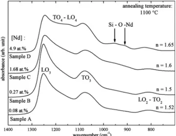
Figure2shows the evolution of the FTIR spectra of the samples annealed at 1100 ° C as a function of the Nd con-centration. One can observe that the LO3 band intensity,
which is constant at low Nd concentrations of 0.08 and 0.27
FIG. 1. Evolution of the FTIR spectra of sample A as a function of the annealing temperature. The spectra were normalized with respect to the TO3
band intensity.
113114-2 Debieu et al. J. Appl. Phys. 108, 113114共2010兲
at.%, significantly decreases while the Nd content was in-creased from 1.68 to 4.9 at.%. This evolution contrasts with the one of the TO4– LO4 pair modes. Indeed, the TO4–LO4
intensity remains constant a low Nd concentrations of 0.08 and 0.27 at.%, then, it progressively increases with increas-ing the Nd content. This shows that the incorporation of Nd generates disorder in the host SiO2matrix.
In the spectral range of 870 to 1000 cm−1, on can
ob-serve a shoulder in the FTIR spectra of the low Nd-doped samples 共A and B兲 which can originate from Si–O− and
Si–OH phonons.23,24However, one can exclude the existence of the Si–OH vibration mode after annealing at 1100 ° C because of the hydrogen desorption. However, the emer-gence of two new weak absorption peaks centered at 910 and 950 cm−1 in the highest Nd-doped sample共sample D兲 sug-gests that other phonons are also optically active in this spec-tral range. These vibration peaks, which are exclusively dis-tinguishable above an annealing temperature of 1100 ° C, are attributed to asymmetric mode of Si–O–Nd bonds.25 They strikingly coincide with the ones observed by several groups in neodymia-silica composites, which, interestingly, con-tained Nd2O3 nanocrystals.28,29 The refractive indexes of
each sample annealed at 1100 ° C are shown in Fig.2. Again, one can observe that the refractive index is rather constant at low Nd concentrations, and significantly increases while the Nd content was increased from 1.68 to 4.9 at.%. The increase in the volume fraction of a Nd2O3phase, which has a refrac-tive index of about 2 would also explain such behavior.26
In Fig.3is depicted the XRD spectra of sample A and D. In sample A, one band corresponding to amorphous SiO2is
observed, while the pattern of sample D indicates the pres-ence of additional phases. In the 27°–32° range, sample D shows various sharp peaks that are located above a band centered at⬃29°. This band, and the 47.5° band, indicate the presence of nanocrystalline Si,22,27 while the sharp and in-tense peaks located at 27.6°, 28.8°, and 30.7° are assigned to Nd2O3 crystals. However, the 28.8° peak may result from
both crystalline Si and Nd2O3, for the sake of completeness.
It is interesting to note that the 27.6° and 30.7° peaks fairly
concur with the ones observed in neodymia-silica composites containing Nd2O3 nanocrystals by several researchers.28,29 As a consequence, the presence of Nd2O3 and Si nanocrys-tals in sample D is clearly established, while such phases are not detected in sample A.
B. PL spectroscopy
Figure 4 shows the evolution of the room temperature PL spectra of sample A as a function of the annealing tem-perature. In the visible domain, sample A shows a broad PL band centered at about 740 nm after annealing. This PL band is originating from quantum-confined excitonic states in Si-np. The enhancement of the PL intensity of this PL band with the annealing temperature is characteristic for Si-np embed-ded in SiO2. It is due to the increase in the Si-np density, as
FIG. 2. Evolution of the FTIR spectra and the refractive indexes as a func-tion of the Nd concentrafunc-tion.
FIG. 3. XRD patterns of samples A and D after annealing at 1100 ° C.
FIG. 4. Evolution of the PL spectra of sample A as a function of the an-nealing temperature.
113114-3 Debieu et al. J. Appl. Phys. 108, 113114共2010兲
showed by the increase in the LO3band intensity in the FTIR spectra 共see Fig. 1兲,22 and the improvement of their passivation,30 as well as the decrease in disorder in the host matrix which provides sources of nonradiative recombina-tion channels, as demonstrated by the decrease in the TO4– LO4pair modes intensity in the FTIR spectra共see Fig.
1兲. Besides, it is generally admitted that 1100 °C is the
op-timal annealing temperature for the PL of Si-np. In the infra-red domain, one can distinguish three peaks centeinfra-red at around 920, 1100, and 1350 nm which correspond to the infra-4f shell transitions of Nd3+ ions from the4F3/2level to the 4I9/2, 4I11/2, and 4I13/2 levels, respectively. The presence of the PL of Nd3+ions after nonresonant excitation brings to light the sensitizing effect of Si-np toward Nd3+ ions.
The Si substrate shows a weak room temperature broad PL band centered at 1130 nm. This band is intrinsic to crys-talline doped-material and is originating from donor or ac-ceptor species. Several authors demonstrated that the PL in-tensity of this band can nonmonotonously vary with the annealing temperature, and furthermore with the doping concentration.31,32Moreover, in our systems, the influence on the deposited layers on the Si substrate properties, in particu-lar at the interface, is still unknown. As a consequence, in order to avoid any mistakes on the evaluation of the PL intensity of Nd3+ ions, we should not take the 4F
3/2→4I11/2
transition into account since its position coincides with the one of the defect PL of the substrate. However that may be, it is clearly seen that the behavior of the PL intensity of Nd3+
ions versus the annealing temperature is manifestly corre-lated with the one of Si-np. Reminding that the PL measure-ments were done under nonresonant excitation, this behavior underlines the strong coupling between Si-np and RE ions, and, accordingly, the potential of sensitizing of Si-np. The increase in the PL intensity of Nd3+is partly explained by the
increase in the Si-np density and by the decrease in disorder which provides sources of nonradiative de-excitation chan-nels of Si-np and Nd3+. The Nd3+ PL intensity is then more efficient after annealing at 1100 ° C.
Figure5shows the behavior of the PL spectra of the thin
films annealed at 1100 ° C as a function of the Nd concen-tration. As the Nd content increases from 0.08 to 0.27 at.%, the PL intensity of Si-np drastically drops and disappears at 1.68 at.%. Then, PL of Si-np surprisingly reappears at the highest Nd concentration of 4.9 at.%. Interestingly, one can observe that the positions and widths of the PL peaks of samples A and B remain identical共see the inset兲; whereas the PL peak of sample D is manifestly shifted to longer wave-lengths. According to the quantum confinement model, the PL of sample D therefore emanates from Si-np that are sen-sibly larger than the ones present in samples A and B; whereas in the latter samples, a change in the density of luminescent Si-np without any modification of the size dis-tribution is observed. In the infrared spectral domain, one can observe that the PL intensity of Nd3+ions drops with the
increase in the Nd concentration.
Figure6 shows the PL spectra of the most luminescent sample under two excitation wavelengths of 266 and 488 nm. One can observe that the three PL peaks of Nd3+ are
similar, whereas the spectra significantly change in the vis-ible domain. Indeed, the visvis-ible PL peak collected after 488 nm excitation is narrower and shifted to longer wavelengths compared to the counterpart recorded under 266 nm tion. In order to better understand this behavior, the excita-tion wavelength dependence of this sample is investigated in the next part of this article using our TPLE system.
C. PL excitation spectroscopy
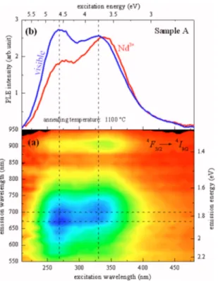
In Fig.7共a兲is shown the TPLE spectral map of sample A. Again, one can clearly recognize the broad visible PL band and an infrared peak that corresponds to the 4F3/2
→4I
9/2transition of Nd3+ions. In the same manner as in Fig.
6, one can observe that the visible PL band recorded at the longer excitation wavelengths is narrowed and shifted to longer wavelengths compared with the ones obtained at shorter excitation wavelengths. As a consequence, it appears
FIG. 5. 共Color online兲 Evolution of the PL spectra as a function of the Nd concentration.
FIG. 6. PL spectra of sample A measured under the 266 and 488 nm exci-tation wavelengths.
113114-4 Debieu et al. J. Appl. Phys. 108, 113114共2010兲
that photons with energies above 4.1 eV are able to excite luminescent species that exhibit light between 600 and 650 nm. In this spectral domain, PL may emanate from residual defect luminescence species in silicates and/or from small Si-np. While photons have excitation energies below 4.1 eV, the PL is mainly originating from excitons confined in Si-np. One can then recognize two maxima at 4.6 and 3.75 eV in the PLE spectrum of the visible PL band关Fig.7共b兲兴. The first one may originate from defect PL, as shown by several re-searchers who studied defects PL共non-bridging oxygen hole centers兲 in silicates,33,34
and/or from small Si-np as obtained from simulations elsewhere,35while the second one is attrib-uted to the recombination of excitonic states in Si-np, as established by many groups.17,36–38
No resonant PL peak of Nd3+was observed in this spec-tral range, as reported elsewhere.17Therefore, no Nd absorp-tion occurs with the excitaabsorp-tion power densities that were used. A comparison of the PLE spectra of the visible emis-sion and the infrared peak is shown in Fig. 7共b兲. It is ob-served that the shapes of the PLE spectra are similar demon-strating that the excitation process of Nd3+ions is manifestly
connected to the luminescent visible species. It is clearly seen that Si-np are the most efficient sensitizers of the PL of Nd3+ions, since the maximum of the PLE spectrum of Nd3+
coincides with the one of Si-np. The presence of a weak 270 nm shoulder in the PLE spectrum of Nd3+ions indicates that
defects states and/or small Si-np play also the same role but to a lesser extent.
IV. DISCUSSIONS
During the annealing, a phase separation occurs leading to the formation of Si-np as shown in the FTIR spectra in
Fig.1. In the same time, it is shown that disorder, which is a potential source of nonradiative channels, decreases in the host silicate matrix. The incorporation of Nd results in the increase in disorder as shown in Fig. 2. As a consequence, the decrease in the PL of Si-np with increasing Nd content 共Fig.5兲 is explained by the raise of energy transfer between
Si-np and Nd3+ ions共which can be luminescent or not兲, and
by the increase in nonradiative recombinations. The Si-np PL quenching due to defects within the Si-np volume induced by the Nd incorporation may be excluded since the solubility of RE in crystalline or amorphous Si is rather low in compari-son with silica.3 Moreover, Fig.3 shows that Nd2O3
nano-crystals are formed at a Nd concentration of 4.9 at.%共sample D兲. The occurrence of such phase in sample D is supported by the progressive increase in the refractive index while the Nd concentration was increased 共Fig.2兲. The presence of a
Nd2O3 phase in the host matrix significantly modifies the
number of oxygen atoms available to form the silicon oxide host matrix consequently leading to the formation of larger Si-np with a higher density. Besides,共see Fig.8兲 the
forma-tion of Nd2O3nanocrystals results in the raise of the average interaction distance between Si-np and Nd atoms 共agglomer-ated or not兲 leading to the occurrence of not-coupled Si-np therefore enable to emit light. This explains the presence of the PL peak of Si-np in sample D 共Fig.5兲 which is
signifi-cantly shifted to longer wavelengths. According to the quan-tum confinement model, longer emission wavelengths are characteristic of larger Si-np. The fact that x-ray pattern of Si nanocrystals were detected in sample D and not in sample A 共Fig. 3兲 may be also due to the modification of the Si-np
density.
The concentration quenching of the PL of Nd3+ions共see
Fig.5兲 is partly explained by cross relaxation processes
be-tween Nd3+ions and neighboring Nd3+ ions or Nd2O3
nano-crystals 共Fig. 8兲 as reported in glass matrices.39,40 This is supported by the existence of Nd2O3 nanocrystals in the
FIG. 7.共Color online兲 TPLE spectral map of sample A 共a兲 and PL excitation 共PLE兲 spectra of the broad visible band and the PL peak of Nd3+ions共b兲.
The PLE spectra were obtained by integrating the broad visible PL band and the PL peak of Nd3+ions.
FIG. 8.共Color online兲 Schematic illustration of a model of the evolution of PL of Si-np Nd3+ions as function of the Nd concentration.
113114-5 Debieu et al. J. Appl. Phys. 108, 113114共2010兲
highest Nd-doped sample. Besides, nonradiative channels in-herent to disorder induced by the Nd incorporation 共Fig.2兲
can be in competition with the energy transfer mechanism between Si-np and Nd3+ions in such nanocomposite systems
leading to the common decrease in the PL intensity of Nd3+
and Si-np, which is in fact observed 共Fig. 5兲. As a
conse-quence, the emission of Nd3+ ions is more efficient while
Si-np are formed, and while the Nd content is low 共0.08 at.%兲. In such conditions, Nd3+ ions benefit from the
sensi-tizing effect of Si-np and from the weak competition of non-radiative recombinations in the host matrix and concentration quenching processes.
TPLE measurement showed that the excitation spectrum of Nd3+ions is clearly correlated with the excitation mecha-nism of Si-np, demonstrating the energy transfer from Si-np toward Nd3+ ions. The efficiency of the energy transfer is maximal at 340 nm which corresponds to the maximum of radiative deexcitation of Si-np.
V. CONCLUSIONS
We have investigated the microstructure and the PL properties of Nd-doped SRSO thin films having the same Si excess. We showed that the maximum of the PL intensity of Nd3+ ions is obtained after annealing at 1100 ° C which cor-responds to the better situation for the achievement of high luminescent Si-np embedded in SiO2, i.e., containing a small
quantity nonradiative recombination channels. We showed that the PL of Nd3+ ions is quenched at high Nd-concentration 共4.9 at.%兲 because of the formation of Nd2O3 nanocrystals and the occurrence of disorder in the host ma-trix. The former participates to the concentration quenching mechanism due to cross relaxation processes, while the latter induced the occurrence of new nonradiative channels which are in competition with the energy transfer mechanism be-tween Si-np and Nd3+ ions. Our TPLE measurements show
that the excitation energy dependence of Nd3+ ions is
non-resonant and follows the one of Si-np. This new result un-ambiguously demonstrates that an energy transfer occurs from Si-np to Nd3+ions.
ACKNOWLEDGMENTS
The authors are grateful to the French-Polish joint project POLONIUM共PHC, EGIDE兲 for their financial sup-port of our work. G. Zatryb and A. Podhorodecki acknowl-edge financial support from fellowship co-financed by Euro-pean Union within EuroEuro-pean Social Fund. The French team thanks the French Agence Nationale de la Recherche, which supported this work through the Nanoscience and Nanotech-nology program 共DAPHNES Project No. ANR-08-NANO-005兲.
1E. Desurvire,Phys. Today47共1兲, 20 共1994兲.
2W. F. Krupke,IEEE J. Quantum Electron.10, 450共1974兲. 3A. J. Kenyon,Prog. Quantum Electron.26, 225共2002兲. 4W. J. Miniscalco,J. Lightwave Technol.9, 234共1991兲. 5A. Polman,J. Appl. Phys.82, 1共1997兲.
6J. H. Campbell and T. I. Suratwala, J. Non-Cryst. Solids263-264, 318
共2000兲.
7J. Wang, L. Reekie, W. S. Brocklesby, Y. T. Chow, and D. N. Payne,J.
Non-Cryst. Solids180, 207共1995兲.
8A. J. Kenyon, P. F. Trwoga, M. Federighi, and C. W. Pitt,J. Phys.:
Con-dens. Matter6, L319共1994兲.
9A. J. Kenyon, C. E. Chryssou, C. W. Pitt, T. Shimizu-Iwayama, D. Hole,
N. Sharma, and C. J. Humpreys,J. Appl. Phys.91, 367共2002兲.
10G. Franzò, V. Vinciguerra, and F. Priolo,Appl. Phys. A: Mater. Sci.
Pro-cess.69, 3共1999兲.
11K. Watanabe, H. Tamaoka, M. Fujii, K. Moriwaki, and S. Hayashi,
Physica E13, 1038共2002兲.
12S.-Y. Seo, M.-J. Kim, and J. Shin,Appl. Phys. Lett.83, 2778共2003兲. 13A. N. MacDonald, A. Hryciw, F. Lenz, and A. Meldrum,Appl. Phys. Lett.
89, 173132共2006兲.
14D. Bréard, F. Gourbilleau, C. Dufour, R. Rizk, J.-L. Doulan, and P. Camy,
Mater. Sci. Eng.146, 179共2008兲.
15D. Bréard, F. Gourbilleau, A. Belarouci, C. Dufour, and R. Rizk,J. Lumin.
121, 209共2006兲.
16F. Gourbilleau, A. Belarouci, D. Bréard, C. Dufour, and R. Rizk,Int. J.
Nanotechnol.5, 574共2008兲.
17A. Podhorodecki, J. Misiewicz, F. Gourbilleau, J. Cardin, and C. Dufour,
Electrochem. Solid-State Lett.13, K26共2010兲.
18C. Ternon, F. Gourbilleau, X. Portier, P. Voivenel, and C. Dufour,Thin
Solid Films419, 5共2002兲.
19S. Charvet, R. Madelon, F. Gourbilleau, and R. Rizk,J. Appl. Phys.85,
4032共1999兲.
20B. J. Hinds, F. Wang, D. M. Wolfe, C. L. Hinkle, and G. Lucovsky,J.
Non-Cryst. Solids227–230, 507共1998兲.
21H. Ono, T. Ikarashi, K. Ando, and T. Kitano, J. Appl. Phys.84, 6064
共1998兲.
22F. Gourbilleau, C. Dufour, M. Levalois, J. Vicens, R. Rizk, C. Sada, F.
Enrichi, and G. Battaglin,J. Appl. Phys.94, 3869共2003兲.
23A. Fidalgo and L. M. Ilharco,J. Non-Cryst. Solids283, 144共2001兲. 24P. Innocenzi,J. Non-Cryst. Solids316, 309共2003兲.
25H. Ono and T. Katsumata,Appl. Phys. Lett.78, 1832共2001兲.
26O. Medenbach, D. Dettmar, R. D. Shannon, R. X. Fischer, and W. M. Yen,
J. Opt. A, Pure Appl. Opt.3, 174共2001兲.
27V. Kapaklis,J. Non-Cryst. Solids354, 612共2008兲. 28
L. KJpiński, M. Zawadzki, and W. Miśta,Solid State Sci.6, 1327共2004兲.
29B. Lal, S. Kumar, P. Aghamkar, S. Rohilla, and D. Singh,Physica B404,
3452共2009兲.
30B. Garrido, M. Lòpez, A. Pérez-Rodríguez, C. García, P. Pellegrino, R.
Ferré, J. A. Moreno, J. R. Morante, C. Bonafos, M. Carrada, A. Claverie, J. de la Torre, and A. Souifi,Nucl. Instrum. Methods Phys. Res. B216, 213共2004兲.
31V. V. Bolotov and V. E. Kan,Physica B404, 4555共2009兲.
32R. K. Ahrenkiel, S. W. Johnston, W. K. Metzger, and P. Dippo,J. Electron.
Mater.37, 396共2008兲.
33M. Cannas, L. Vaccaro, and B. Boizot, J. Non-Cryst. Solids 352, 203
共2006兲.
34L. Skuja,J. Non-Cryst. Solids239, 16共1998兲. 35C. Bulutay,Phys. Rev. B76, 205321共2007兲.
36A. Podhorodecki, J. Misiewicz, F. Gourbilleau, and R. Rizk,Electrochem.
Solid-State Lett.11, K31共2008兲.
37Y. H. Xie, W. L. Wilson, F. M. Ross, J. A. Mucha, E. A. Fitzgerald, J. M.
Macaulay, and T. D. Harris,J. Appl. Phys.71, 2403共1992兲.
38S. Sinha, S. Banejee, and M. Arora,Phys. Rev. B49, 5706共1994兲. 39J. A. Caird, A. J. Ramponi, and P. R. Staver,JOSA B8, 1391共1991兲. 40C. Jacinto, S. L. Oliveira, L. A. O. Nunes, M. J. Myers, and T. Catunda,
Phys. Rev. B73, 125107共2006兲.
113114-6 Debieu et al. J. Appl. Phys. 108, 113114共2010兲