HAL Id: tel-01281330
https://tel.archives-ouvertes.fr/tel-01281330
Submitted on 2 Mar 2016HAL is a multi-disciplinary open access
archive for the deposit and dissemination of sci-entific research documents, whether they are pub-lished or not. The documents may come from teaching and research institutions in France or abroad, or from public or private research centers.
L’archive ouverte pluridisciplinaire HAL, est destinée au dépôt et à la diffusion de documents scientifiques de niveau recherche, publiés ou non, émanant des établissements d’enseignement et de recherche français ou étrangers, des laboratoires publics ou privés.
micro and optoelectronic applications
Viktoriia Gorbenko
To cite this version:
Viktoriia Gorbenko. Ion beam characterisation of III-V heterostructures for micro and optoelectronic applications. Micro and nanotechnologies/Microelectronics. Université Grenoble Alpes, 2015. En-glish. �NNT : 2015GREAT140�. �tel-01281330�
THÈSE
Pour obtenir le grade de
DOCTEUR DE LA COMMUNAUTÉ UNIVERSITÉ
GRENOBLE ALPES
Spécialité : NANOELECTRONIQUE ET NANOTECHNOLOGIES
Arrêté ministériel : 7 août 2006
Présentée par
Viktoriia Gorbenko
Thèse dirigée par Thierry Baron
Co-encadré par Jean-Paul Barnes (CEA-LETI) et Franck Bassani
(LTM-CNRS)
Préparée au sein du Service de Caractérisation des Matériaux & Composants du LETI et du Laboratoire des Technologies de la microélectronique du CNRS au CEA-Grenoble.
dans l’Écoles Doctorale EEATS
Caractérisation par faisceaux d’ions
d’hétérostructures
III-V
pour
les
applications micro et optoélectroniques
Thèse soutenue publiquement le 18 Décembre 2015, devant le jury composé de :
Dr. Michel Gendry
Directeur de Recherche, INSA de Lyon, Président
Dr. Brice Gautier
Professeur des Universités, INSA de Lyon, Rapporteur
Dr. Thierry Conard
Ingénieur-chercheur, IMEC, Belgique, Rapporteur
Dr. Thierry Baron
Directeur de Recherche, LTM, CNRS, Directeur de thèse
Dr. Franck Bassani
Chargé de Recherche, LTM, CNRS, Co-encadrant de thèse
Dr. Jean-Paul Barnes
5
ABSTRACT
The integration of III-V semiconductor compounds on silicon should lead to the development of new highly efficient micro- and optoelectronic devices. High mobility InGaAs material is a promising candidate for n-channel metal-oxide-semiconductor-field-effect transistor beyond the 10 nm technology node. Moreover, III-V semiconductors are also suitable materials for fabrication of optical (lasers, diodes) and ultra-high frequency analog devices and their integration on a Si platform will add new functionalities for optical networks and communication. However, the miniaturization of devices and their integration into 3D architectures require the development of advanced characterization methods to provide information on their physico-chemical composition with nanometer scale resolution.
In this thesis, the physico-chemical studies of III-V heterostructures directly grown on 300 mm Si wafers by metalorganic vapor phase epitaxy are addressed. Secondary ion mass spectrometry (SIMS) techniques are used and developed in order to study interface abruptness, chemical composition and doping of III-V thin layers in 2D and 3D architectures with high depth resolution. The accurate quantitative analysis of InGaAs quantum wells (QWs) in 2D and 3D architectures was performed using magnetic SIMS and Auger techniques. To obtain the chemical profiling of narrow and repetitive III-V structures, an averaging profiling method was developed for both techniques. Additionally, 3D reconstruction and depth profiling of individual trenches (less than a hundred nanometers in width) containing thin InGaAs QWs selectively grown in silicon dioxide cavities using the aspect ratio trapping method were successfully obtained using Time-of-flight SIMS and atom probe tomography. Finally, the results were correlated with photoluminescence measurements.
KEYWORDS: III-V heterostructures, SIMS, FinFET, microelectronics, optoelectronics, and quantum wells
7
RÉSUMÉ
L'intégration de composés semi-conducteurs III-V sur silicium devrait conduire au développement de nouveaux dispositifs micro- et optoélectroniques performants. Le composé InGaAs de haute mobilité électronique est un candidat prometteur pour le transistor métal-oxyde-semiconducteur à effet de champ à canal n au-delà du nœud technologique 10 nm. En outre les semi-conducteurs III-V sont aussi des matériaux appropriés pour la fabrication de composants optiques (lasers, diodes) et de dispositifs analogiques ultra-haute fréquence et leur intégration sur une plateforme Si ajoutera de nouvelles fonctionnalités pour le réseau de communications optiques. Cependant la miniaturisation des dispositifs et leur intégration dans les architectures 3D nécessitent le développement de méthodes de caractérisation avancées pour fournir des informations sur leur composition physico-chimique avec une résolution à l'échelle nanométrique.
Dans cette thèse, les études physico-chimiques des hétérostructures III-V directement élaborées sur plaquettes de Si 300 mm par épitaxie en phase vapeur sont adressées. Les techniques de spectrométrie de masse d'ions secondaires sont utilisées et développées dans le but d'étudier la raideur des interfaces, la composition chimique et le dopage de couches III-V minces dans des architectures 2D et 3D avec une bonne résolution en profondeur. L'analyse quantitative précise sur un puits quantique InGaAs (PQ) pour des architectures 2D et 3D a été réalisée en utilisant les techniques SIMS magnétique et Auger. Pour obtenir le profil chimique des structures III-V étroites et répétitives, une méthode de moyenne des profils a été développée pour ces deux techniques. Egalement, la reconstruction 3D et le profil en profondeur de tranchées individuelles (moins de cent nanomètres de largeur) contenant un PQ d’InGaAs mince obtenu par croissance sélective dans des cavités de dioxyde de silicium en utilisant la méthode de piégeage des défauts par rapport d’aspect ont été obtenus avec succès en utilisant le SIMS à temps de vol ainsi que la sonde atomique tomographique. Enfin, les résultats ont été corrélés avec des mesures de photoluminescence.
MOTS-CLÉS: III-V hétérostructures, SIMS, FinFET, microélectronique, optoélectronique, puits quantique
9
L'expérience est une lanterne acrochée dans le dos qui n'éclaire que le chemin parcouru ...
11
ACKNOWLEDGMENTS
I believe that with an expert guidance everything is possible. I would like to thank the supervisors of my thesis, Dr. Jean-Paul Barnes and Dr. Franck Bassani, for patience, support and guidance in writing of the thesis. I very appreciate their contributions, discussions and advices in the research work (conferences, publications, seminars, symposiums etc.). I am grateful for (English and French) language revision of my thesis. I would like to thank the director of my thesis, Dr. Thierry Baron, for expert guidance of my thesis and great positive mood all the time. I was lucky to work with one of the kindest and friendliest supervisors. I thank the Material Integration team at LTM-CNRS Laboratory for great teamwork in MINOS project, scientific discussions concerning growth of materials, and nice friendly working atmosphere. Especially I would like to mention the Romain Cipro(soon Dr), Dr. Mickael Martin, and Arnaud Alcoud for providing the samples and great discussions together. Thanks to Dr. Yann Bogumilowicz for his advices for my thesis.
I would like to thank also the Nanocharacterization group at LETI-CEA for great support and very friendly atmosphere. I thank Dr. Marc Veillerot and Dr. Alexandre Merkulov (from Cameca) for their advices and training in working with SIMS SC Ultra instrument. I was working with the great international team. Especially I would like to mention my colleagues with whom I shared my office: Riccardo, Robert and Tanguy. Three years of working together have passed so fast. Thanks them for all fantastic time, coffee breaks (who can do research without café ?!!), lunch time, many different discussions (scientific and non-scientific) and for all great Ph.D. moments.
I am grateful to Dr. Adeline Grenier, Dr. Sylvain David and Dr. Guillame Audoit for FIB-STEM and APT experiments, Dr. Francois Pierre for RBS experiments. I am thankful to Dr. Wael Hourani for many discussions concerning Auger experiments, as well for his support and help. I am grateful to Dr. Dennis Mariolle and Dr. Lukasz Borowik for advices concerning AFM measurements and pleasant working time together. Thanks to my dear colleagues and friends Dr. Camille Marie, Dr. Agniezka Priebe, Dr. Ferrah Djawhar, and Mariana Verezhak (soon Dr.) for their help in preparation of the Ph.D. defense and, in general, for all support and shared sports activities (ski, swimming, ice-skating etc.).
Thanks to LTM and LETI administration, Dr. Jean-Claude Royer, Dr. Francois Bertin and Dr. Gambacorti Narciso for their help and advices in my research work.
It was a great pleasure to work with you. Merci à tous!
My deepest thanks and gratitude I wish to express to my wonderful family. I am happy to have you, my dear sister Nataliya (Dr.), brother Ivan (maybe a future Dr.), father Vitalij (Dr.) and mother Iryna(Mother).
13
CONTENTS
ABBREVIATION INDEX ... 15
CHAPTER I INTRODUCTION AND OVERVIEW ... 19
I.1. III-V materials as channel materials... 22
I.2. State of the art of III-V integration on Si substrate ... 24
. Challenges of nano-characterization of channel materials in 2D and 3D architectures 28 I.2 I.2.1 Doping profiling in 3D architecture materials ... 28
I.2.2 SIMS profiling of InGaAs materials overview ... 30
CHAPTER II Growth of III-V heterostructures and characterization methods ... 35
Growth of III-V heterostructures on Si wafers by MOCVD ... 35
II.1 II.1.1 The basic principles of the MOCVD technique ... 35
II.1.2 MOCVD reactor ... 37
II.1.3 Challenges of III-V growth on Si wafers ... 37
II.1.4 Sample description ... 39
II.1.4.1 InGaAs/AlAs quantum wells on planar Si substrates ... 39
II.1.4.2 InGaAs reference samples for quantitative SIMS analysis ... 41
II.1.4.3 Selective growth of III-V heterostructures on non-planar Si-substrates by MOCVD ... 43
II.1.4.4 Doping in planar and non-planar samples ... 44
Ion beam characterization techniques ... 45
II.2 II.2.1 Secondary ion mass spectrometry ... 45
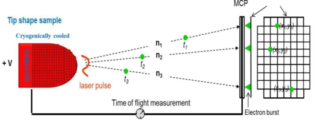
II.2.1.1 Time of flight mass spectrometry ... 46
II.2.1.2 Experimental conditions ... 47
II.2.1.3 Magnetic sector SIMS ... 47
II.2.1.4 Instrumentation of Cameca SC-Ultra magnetic SIMS ... 49
II.2.1.5 Experimental conditions ... 51
II.2.1.6 Depth calibration ... 53
II.2.2 Atom probe tomography ... 53
II.2.2.1 Sample preparation for APT using the focused ion beam technique ... 55
II.2.2.2 Experimental conditions ... 57
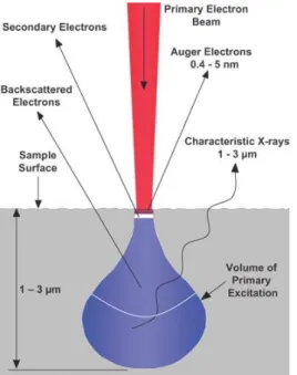
II.2.3 Auger technique ... 57
14
II.2.4 Rutherford backscattering spectrometry ... 60
II.2.4.1 Experimental conditions ... 62
CHAPTER III Quantitative chemical analysis of III-V elements using SIMS ... 65
. Theoretical aspects of quantitative SIMS analysis ... 65
III.1 . Description of reference standards for accurate measurements of composition in III.2 InxGa1-xAs and AlxGa1-xAs matrices... 68
III.2.1 Ion-implanted standards ... 68
III.2.2 Standards for accurate measurements of x in InxGa1-xAs matrix ... 70
Development of a SIMS protocol for InGaAs channel material ... 74
III.3. III.3.1 Quantitative analysis of InGaAs QW using O2+ ion beam bombardment ... 74
III.3.2 Quantitative analysis of InGaAs quantum well using SIMS ... 82
III.3.3 Quantitative analysis of InGaAs quantum well using complementary techniques84 III.3.4 Quantification using molecular MCs+ ions under low energy sputtering ... 86
Development of a SIMS protocol for n-doped GaAs in 2D and 3D architectures ... 88
III.4 . CHAPTER IV Development of experimental protocols for chemical composition profiling of 3D architecture structures ... 99
IV.1 .Recall of basic parameters of the investigated sample ... 99
IV.2. An average approach using low energy magnetic SIMS ... 99
IV.2.1 SIMS conditions optimization in terms of sample topography and depth resolution under oxygen ion beam bombardment ... 100
Effect of primary energy ... 100
IV.2.1.1 Effect of orientation of the ion beam with respect to the trenches ... 102
IV.2.1.2 Effect of incidence angle ... 107
IV.2.1.3 Effect of sample rotation ... 109
IV.2.1.4 IV.3 3D reconstruction of a single III-V trench using ToF-SIMS and atom probe tomography ... 116
IV.4 Quantitative analysis of InGaAs quantum well by Auger and SIMS techniques121 CONCLUSIONS ... 128
PERSPECTIVES:... 131
15
ABBREVIATION INDEX
AES Auger electron spectroscopy
AFM Atomic force microscopy
AMAT Applied Materials Tool
APB Anti-phase boundary
APD Anti-phase domain
APT Atom probe tomography
AR Aspect ratio
ART Aspect ratio trapping
BOX Buried-oxide
CELO Confined epitaxial lateral overgrowth
CMOS Complementary metal-oxide-semiconductor technology
CVD Chemical vapor deposition
DWB Direct wafer bonding
EM Electron multiplier
ESA Electrostatic sector analyzer
EXLIE Extremely low primary beam impact energy
FC Faraday cup
FIB Focused ion beam
FinFET Fin-shaped field-effect transistor
FWHM Full-width at half-maximum
HF Hydrogen fluoride
IC Integrated circuit
16
LED Light-emitting diode
LTE Local thermal equilibrium
MBE Molecular beam epitaxy
MOCVD Metalorganic chemical vapor deposition
MOSFET Metal-oxide-semiconductor field-effect transistor
NW Nanowires
PIGE Particle induced Gamma-Ray emission
PIXE Particle induced X-ray technique
PL Photoluminescence
QW Quantum well
RBS Rutherford backscattering spectrometry
RF Radio frequency
RMS Root mean square
RSF Relative sensitivity factor
SF-SIMS Self-focusing SIMS
SIMS Secondary ion mass spectrometry
SR Sputter rate
STEM Scanning transmission electron microscope
STI Shallow trench isolation
TEGa Triethylgallium
TEM Transmission electron microscopy
TMAl Trimethylaluminium
TMGa Trimethylgallium
ToF-SIMS Time-of-flight SIMS
17
XRD X-ray diffraction
19
CHAPTER I
I. INTRODUCTION AND OVERVIEW
Over the past fifty years, the miniaturization of circuits by transistor scaling remains the main technology trend in the semiconductor industry [W. Arden et al., 2004]. The International Technology Roadmap for Semiconductors (ITRS) [www.itrs.net] according to Moore’s law defines the continuous downscaling of integrated circuits (IC) by a factor 0.7 every two years. Moore’s law states that the number of IC components increases exponentially over time. It requires the improvement of the performances, i.e. increasing the speed and the power of transistors, whilst reducing the cost per transistor. Thus, it has a big influence on the semiconductor market as it provides a benchmark for semiconductor manufacturing.
The semiconductor benchmarking is accompanied by the continuous studies of material properties. The research goal is to find alternative semiconductor compounds with the best physical features with low-cost semiconductor manufacturing. Silicon has high mechanical strength and extremely high-quality in comparison with other materials (e.g. GaAs, InP). For this reason, a silicon-based manufacturing replaced the first established germanium-based device industry. Thus, large-scale devices, such as GaN or InGaN-based light-emitted diodes (LED), III-V laser diodes and transistors can be integrated (co-integrated) on large-area silicon wafers (300 mm, 450 mm in near future).
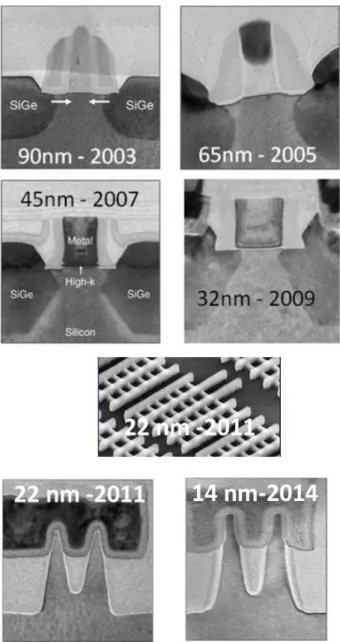
The evolution of complementary metal-oxide-semiconductor (CMOS) technology over the last fifteen years is illustrated in Figure I-1. However, the device scaling revealed new challenges in transistor manufacturing. The reduction of the operation voltage has to be considered in order to solve the issue of power dissipation in logic chips. [J. A. del Alamo, 2011]. Also, the switching speed has to be accordingly adjusted. The transistor performance, in general, has to be improved, thus, issues of channel mobility, electrostatic control, parasitic resistance and gate capacitance are still important for device performance [K. J. Kuhn, 2012]. Further scaling of transistors was made possible recently by the introduction 3-dimensional (3D) device architectures. Such architectures may take the form of the fin-shaped field-effect transistor (FinFET), TriGate, and Gate-all-around transistors [K. J. Kuhn, 2012]. Moreover, FinFET and TriGate transistors were recently manufactured by Intel for the 22-nm and 14-nm node CMOS technology, respectively (see Figure 1-1).
The integration of III-V semiconductors on Si wafers in 3D architectures will give new functionalities in opto- and microelectronic applications. Furthermore, III-V materials have interesting physical properties, such as a high carrier transport, direct and wideband gap. However, the integration of III-V on Si faces growth-related challenges, i.e. a thermal and lattice mismatches of semiconductors, which affect the device operation. The growth and characterization of III-V semiconductors grown on planar and non-planar Si substrates using ion beam techniques are addressed in this thesis and presented in the following four chapters.
20
Figure I-1 CMOS scaling evolution from 90 nm to 14 nm technology node. Prototypes are demonstrated by Intel company [K. J. Kuhn, 2012, M. Bohr, 2014].
Chapter I introduces the III-V integration technology on Si wafers. The first section
describes the physical properties of III-V materials that make them suitable for opto- and micro-electronics applications. In particular, the main application of III–V materials on Si is described and their use as channel materials in nMOSFETs technology. It reports on the III-V FinFET and FDSOI technology issues. The most promising and recently reported approaches to integrating III-V on Si wafers, such as direct wafer bonding, lateral overepitaxy, and aspect ratio trapping are described. The second section focuses on the characterization issues of materials in 3D architectures. It summarizes the very recently reported works regarding 3D doping profiling and chemical profiling of thin InGaAs layers.
Chapter II describes the growth and characterization techniques and also the samples
investigated in this thesis. The first section of this chapter is focused on the epitaxial growth process of III-V heterostructures on 300 mm Si wafers using MOCVD. The challenges and
21
methods to obtain high-quality III-V layers on Si wafers are addressed. The description of InGaAs quantum wells (QW) and Si-doped GaAs samples grown by MOCVD studied using magnetic secondary ion mass spectrometry (SIMS) and Time-of-flight (ToF) SIMS is given. The first section includes also the description of reference sample used for quantitative analysis. The second section is focused on the ion beam techniques used in this work. It starts with a description of the basic principles of magnetic SIMS and ToF-SIMS followed by the details of the Cameca SC-Ultra instrument used in this work. Then the basic principles of atom probe tomography (APT), Auger and Rutherford backscattering spectrometry (RBS) are explained. Moreover, at the end of each sub-section, the experimental details for each technique are given.
Chapter III is focused on the compositional analysis of InxGa1-xAs QWs and 3D-doping
profiling using SIMS for future generations of transistors. It starts with theoretical background on the quantitative analysis using SIMS. The development of SIMS protocols under oxygen and cesium ion beam sputtering under low impact energy is described. Quantitative analysis using reference InxGa1-xAs series designed in this thesis is explained. Moreover, the ion yield
as a function of indium fraction x and primary energy of ion beam is experimentally determined. Quantitative analysis using MCs+
ions was also demonstrated. Finally, the development of SIMS and ToF-SIMS protocols for Si-dopant profiling in 2D and 3D architectures is described.
Chapter IV reports on the investigation of repetitive III-V trench arrays selectively grown by
MOCVD on patterned Si wafers. The first section of this chapter introduces the average approach for chemical depth profiling of repetitive array of III-V trenches. This section describes also the optimization and development of the SIMS conditions used to profile the III-V trench arrays. SIMS parameters, such as (1) the impact of primary energy, (2) incident angle and (3) orientation of the ion beam with respect to the trenches are investigated in detail in order to improve the depth resolution. Investigation of topography formation under oxygen irradiation on III-V materials using atomic force microscopy observations and correlation with SIMS profiles is also included. The second section describes 3D chemical profiling of thin InGaAs QWs grown on patterned Si wafers using ToF-SIMS and APT techniques. This section represents the complementary studies performed on individual III-V trench arrays using the pointed and average analysis method by Auger technique. Finally, the quantitative chemical analysis for repetitive InGaAs QWs arrays studied using Auger, SIMS, photoluminescence techniques are described.
The conclusions and perspectives summarize the main results obtained in this thesis and outline the perspectives for this work in terms of characterization of III-V semiconductors for advanced CMOS technology.
22
III-V materials as channel materials
I.1
III-V semiconductors are promising materials for realization of high performance of metal-oxide-semiconductor field effect transistor (MOSFET) and will be manufactured starting from 2018 according to ITRS 2013 roadmap [www.itrs.net]. Integration of high mobility III-V materials is essential for increasing the transistor performance with a reduction in voltage [J. A. del Alamo, 2011]. The carrier mobility of III-V semiconductor compounds is illustrated in Figure I-2. As can be seen, III-As based components exhibit an electron mobility (>8000 cm2/Vs) ten times higher than silicon, while III-Sb based components have a hole mobility in the same order than germanium. Thus, the replacing of silicon channels by InGaAs or InAs materials will allow transistor performance to be improved.
Figure I-2 Electron and hole mobility versus a lattice constant of III-V group compounds, where the highest room-temperature mobility of holes and electrons are marked in blue and red color, respectively. Figure is taken from reference [J. A. del Alamo, 2011].
Due to direct and wide band gap (~1-2.2 eV), III-V materials are also often used for fabrication of optoelectronic devices, such as lasers, diodes etc. For example, III-nitride-based LEDs are commonly used in general lighting, traffic signals, video displays, sensors, etc. Moreover, the heterogeneous integration of III-V on Si will make the manufacture of various semiconductor chips possible [J. A. del Alamo, 2011]. Applications of III-V materials in high electron mobility transistor (HEMT) and Si photonics are promising for data transfer by combining systems with a cell phone, TV and Internet together [T. Li et al., 2011]. Additionally, III-V materials (e. g. GaN) can be used in solar cells and high-power/high-frequency transistors (broadcast, wireless infrastructure, defense). The main application of the
23
III–V materials on Si is, however, the high-speed devices in nMOSFETs technology [G. Doornbos et al., 2010] and is discussed below.
As an example, the structure of III-V nMOSFET (NMOS) and Ge pMOSFET (PMOS) in CMOS technology are illustrated in Figure I-3. As was mentioned previously, III-V and Ge materials have to be integrated on Si substrates, however, such issues need to be solved for CMOS technology: (i) growth of high-quality III-V and Ge materials on Si substrates, (ii) interface quality between gate insulator and channel material, (iii) formation of low resistivity source/drain contacts [S. Takagi et al., 2007, S. Takagi et al., 2013].
Figure I-3 CMOS device structure of III-V nMOSFET and Ge pMOSFET. Figure is taken from reference [S. Takagi et al., 2013].
The integration of the gate on III-V is challenging. Possible planar quantum well (QW) MOSFET designs are illustrated in Figure I-4 a, b. The advantages having the channel localized under the source and drain (see Figure I-4 a) are process flexibility and possibility to obtain high mobility transport in the device. In this device, the dielectric/III-V interface is created later in the process. It allows the uniaxial strain in the channel to be introduced. Promising results of electrical characteristics of planar QW MOSFET devices were reported by R. Terao [R. Terao et al., 2011]. However, scaling of the planar QW MOSFET requires a very thin channel (less than 10 nm) and extremely thin gate barrier which is difficult to achieve. Additionally, the quantum confinement in silicon or III-V may be critical for devices with a thickness less than 5 nm. It may lead to increasing the threshold voltage (VT) and
changes in the scattering behavior (transport of electrons). [K. J. Kuhn, 2012]. Therefore, alternative device designs (Figure I-4 c, d), e.g. III-V FinFET or Gate-all-around nanowires, are designed to improve the electrostatics in MOSFETs. In such devices, the III-V channel is surrounded with two or more opposing gates to improve the short-channel control. Moreover, the effective channel length λN can be improved by increasing the number of gates, decreasing
the gate dielectric thickness and channel thickness, or by decreasing the permittivity of the channel [K. J. Kuhn, 2012].
24
Figure I-4 Architecture of MOSFETs based on the III-V channel materials, where a) etched source-and-drain QW MOSFET, b) regrown source-and-drain QW MOSFET, c) III-V FinFET, d) Gate-all-around nanowire MOSFET. Figure is adapted from reference [J. A. del Alamo, 2011].
Further, such architectures as Pi-Gates (the side gates extend below the channel) and Omega-FETs (the gate wraps the top and surrounds the part of the fourth side) can be mentioned for future integration of III-V channel materials [K. J. Kuhn, 2012]. However, prototypes of such III-V devices were not yet developed.
State of the art of III-V integration on Si
I.2
The growth of III-V compounds on Si has been studied for over 30 years. The growth of high-quality III-V on Si remains challenging due to the thermal coefficient mismatch and large lattice mismatch between III-V materials and Si. The large lattice mismatch leads to the formation of misfit dislocations with high density which results in the degradation of devices performance. Moreover, thermal expansion coefficient difference might cause additional strain in the layers, even the presence of cracks in thick layers (see Chapter II). Thus, to overcome these issues and to integrate III-V on silicon different methods were developed and are discussed below.
The first approach is based on the direct wafer bonding (DWB) process similar to the silicon-on-insulator (SOI) technology. InGaAs on donor InP wafers are used to fabricate InGaAs channels on SOI. The fabrication process of an InGaAs layer of 3 nm in thickness with a
25
lattice matched InP on Si by molecular beam epitaxy (MBE) is illustrated in Figure I-5a [S. Takagi et al., 2013]. Figure I-5b shows a transmission electron microscopy (TEM) image of a good quality InGaAs-OI layer with the smooth and abrupt interfaces. For buried-oxide (BOX) layers, the Al2O3 thin films of 7.7 nm were used to integrate III–V-OI on Si wafers. High
electron mobility in the range of 2000-3000 cm2/Vs for the 450 nm in thickness In53GaAs-OI
has been reported using this approach [X. Dai et al., 2014].
Figure I-5 a) Fabrication process of InGaAs-OI substrates, b) cross-sectional TEM image of InGaAs-OI on Si wafers. Figure is taken from reference [S. Takagi et al., 2013].
The fabrication of ultrathin InAs on SOI was also reported. Firstly, GaSb donor substrates with an AlGaSb sacrificial etch layer and InAs active layer with PMMA are used. Then, active layers are patterned into nanoribbons and the sacrificial layer is partially etched. Finally, the thin InAs films are transferred on SiO2/Si substrates. (see Figure I-6). The main
challenges of SOI integration are issues of scaling up to large wafers (300 mm or 450 mm in future) and the high cost of device fabrication [J. A. del Alamo, 2011].
Figure I-6 a) Fabrication process of InAs with silicon-on-insulator (SOI) technology. The epitaxially grown, single-crystal InAs films are patterned with PMMA and wet etched into nanoribbon arrays. A subsequent selective wet etch of the underlying AlGaSb layer and the transfer of nanoribbon arrays by using an elastomeric PDMS slab result in the formation of InAs nanoribbon arrays on Si/SiO2 substrates. Figure is taken from reference [H. Ko et al.,
26
A second approach is based on the selective heteroepitaxial growth of high-quality III-V channel materials using the aspect ratio trapping (ART) or necking effect approach (see Chapter II.1.3). The reduction of dislocation density at Si1-xGe/Si interfaces by selective
growth in small areas of patterned Si substrates by chemical vapor deposition (CVD) was demonstrated in 1990. [D. B. Noble et al., 1990] After twenty years, the growth of lattice-mismatched materials like GaAs (Figure I-7 a, b) [Y. Q. Wu et al., 2008, Z. Zuoming et al., 2009], Ge [J.-S. Park et al., 2009] and InP [C. Merckling et al., 2013] on patterned silicon wafers was successfully demonstrated. For selective epitaxial growth of III-V materials on Si, an MOCVD technique is mainly used [C. Merckling et al., 2013, R. Castillo Ojeda et al., 2007, G. Wang et al., 2010]. The InP growth in shallow trench isolation (STI) on patterned Si (001) with a width in the range of 40 to 500 nm using selective epitaxial growth was demonstrated using the ART method [C. Meckling, 2013]. The dislocations that are generated at the III-V/Si substrate are trapped in the SiO2 walls and therefore, reducing the number of
dislocations and providing high-quality material near the top surface. The high-quality of III-V materials on Si wafers in STI structures can be achieved with an aspect ratio (AR) more than 2 [J. G. Fiorenza et al., 2010]. However, the extreme scaling of the trench width down to 15 nm is challenging and requires the optimization of growth conditions (pressure, temperature) to obtain good growth uniformity and crystal quality [C. Merckling et al., 2013]. Rapid melt growth method is another method to overcome a large mismatch of materials. It is based on the deposition, patterning of amorphous GaAs and, therefore, its transformation to a single crystal by melting and solidifying on Si substrates.[C. Shu-Lu et al., 2010]
Figure I-7 a) Diagram of epitaxy GaAs on a SiO2 patterned silicon substrate using ART
method, b) cross–section STEM image of GaAs. Figure is taken from reference [Y. Q. Wu et al., 2008].
Lateral epitaxial overgrowth approach was demonstrated by several groups [Takagi, 2007, [W. Yang et al., 1999, Y. Honda et al., 2002]. This method is based on III-V growth in the limited areas inside of SiO2 windows and is illustrated in Figure I-8. Similar to ART method
the dislocations are geometrically confined in SiO2 walls and as the result, the high-quality
III-V materials can be achieved. The relative high electron mobility (µ480 cm2/V) using a similar approach (ART and overepitaxy or overgrowth) were demonstrated by Y. Q.Wu [Y. Q. Wu et al., 2008]. The challenges of this method are a reduction of defects (point and antiphase domains), thickness control under ultra-thin regime and control of surface flatness and edge shapes of III–V-OI films [S. Takagi et al., 2007].
27 Figure I-8 Diagram of lateral epitaxial overgrowth.
Very recently the gate first-aligned FinFET device using a confined epitaxial lateral overgrowth (CELO) was demonstrated [L. Czornomaz et al., 2015]. A high-quality In0.7GaAs
on Si materials and as a result, the good device performance was achieved using this method. Figure I-9 a, b, c shows that the fabrication process of InGaAs material by necking the defects in the seed region.
Figure I-9 a) Plan view of the corresponding InGaAs CELO structure, b, c) cross-sectional HR-TEM image confirming that defects are confined in the seed region. Figure is taken from reference [L. Czornomaz et al., 2015].
The first prototype of III-V FinFET devices monolithically integrated on 300 mm Si wafers was demonstrated by IMEC group in 2014 [http://www2.imec.be]. Figure I-10 shows the TEM image of high-quality InGaAs layer capped on an InP trench with a width less than 40 nm using ART method. However, the reduction of trench width (less than 40 nm) requires the progress in patterning technology and growth parameters optimization.
Figure I-10 TEM image of first III-V FinFET devices monolithically integrated on 300 mm Si wafers [http://www2.imec.be].
The semiconductor roadmap for 28 nm devices and beyond is focused mainly on FinFET and FD-SOI technology. SOI Industry Consortium [http://www.soiconsortium.org/] includes such companies as IBM, IMEC, SOITEC, Freescale, GlobalFoundries. The good cost-to-performance ratio is an important parameter for the semiconductor industry. FD-SOI wafers
28
are expensive but the integration of devices is found to be very efficient for low power devices. However, the highest performance was achieved with FinFET devices. Recently, the combination of FinFET with SOI was demonstrated as a possible integration approach for III-V channels for 16 nm and 7 nm nodes. The TEM image of this device is shown in Figure I-11. Thus, the different integration approaches of III-V materials on Si platform were developed.
Figure I-11 TEM image of FinFET on SOI device. Figure is taken from [http://www.eetimes.com/document.asp?doc_id=1327035&].
Challenges of nano-characterization of channel materials in 2D and 3D
I.3
architectures
I.3.1 Doping profiling in 3D architecture materials
The control of doping is an important issue to achieve high-performance transistors. To obtain the doped source/drain region, ion implantation, vapor phase doping or plasma immersion doping processes are used. The doping process requires the dopant profile optimization (conformal doping) of the source/drain area [J. Mody et al., 2010]. However, the control of dopants incorporation, activation, and self-diffusion in 3D devices is difficult. That’s why an improved metrology characterization should be developed for optimization of this doping process. Here, the recently reported metrology for doping measurements in 3D structures/materials is discussed.
Dynamic SIMS is often used to study the doping profiling (e.g. dopant concentration and diffusion) in planar materials due to its excellent sensitivity. SIMS allows the total concentration of dopants to be estimated while techniques such as photoluminescence, Raman spectroscopy, and photoconductivity and scanning photocurrent microscopy and scanning capacitance will give only qualitative information on measured impurities. Additionally, the dopant activation can be studied in a combination in a combination with Hall measurements which give carrier concentration.
29
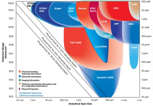
High lateral resolution (less than 40 nm) and high sensitivity of detection (less than 1·1017
at/cm3) are required to study the doping in 3D structures. However, most analytical techniques have to be improved in order to provide an accurate quantitative information of dopants in small areas(see Figure I-12). Recently, despite the low SIMS lateral resolution (less than 100 nm) but thanks to its high sensitivity of detection the promising results of doping measurements in 3D structures were reported.
Figure I-12 Analytical resolution versus detection limit for a variety of standard characterization techniques in material research. Figure is taken from [www.eag.com]
Promising results of doping profiling in vertical III-V nanowires (NWs) by profiling ensembles were demonstrated [A. C. E. Chia et al., 2013]. For SIMS experiments, the Cyclotene polymer was used to fill the space between NWs to achieve a smooth and planar top surface. Using the similar approach the doping profiling in fins for FinFET technology was recently reported [W. Vandervorst et al., 2014]. Note that, identical doping distribution (profile) on the top and at the side of fins is required for FinFET technology to optimize the electrical performance of the device. For SIMS experiments, the spaces between the fins were filled by polysilicon and then, the top of the surface was planarized by polishing. SIMS method for fin structures is based on the assumption that recorded SIMS signal from arrays always corresponds to an amount of dopants present at the instantaneous surface [W. Vandervorst et al., 2014]. Figure I-13 illustrates the SIMS profile of B-implantation in fin arrays of 80 nm in width with a doping concentration of 6-7·1021 at/cm3. To detect dopant in fins structures, the cluster ions can be also used. The Cs2As+ cluster ions using averaging the
fins ensembles were used to detect the As doping concentration in FinFETs. [K. A. B. T. Meura et al., 2014].
30
The results of dopant clustering and dopant diffusion in FinFET devices were reported using APT technique with high spatial resolution [A. K. Kambham et al., 2013 ]. The non-conformality of the doping process and the different dopant gradients under the gate at the top and the sidewalls were observed. Overall, APT is a useful technique which gives the information from the very small volume. However, APT analysis of dopants in fins is, in general, difficult due to challenges of sample preparation, poor tip yield, artifacts during the reconstructions and differences in the in the evaporation field of semiconductor/insulator etc. [W. Vandervorst et al., 2014]. Moreover, the main disadvantage of APT compared to SIMS is lower sensitivity of detection. Additionally, there is a need to obtain the dopant information from a large number of fins to optimize the dopant process. Thus, it seems that SIMS is the most adapted technique for doping profiling in 3D devices.
I.3.2 SIMS profiling of InGaAs materials overview
As was mentioned previously, InGaAs materials are promising high-mobility materials for nMOSFET devices. InGaAs materials grown on Si using the ART approach can be formed ready to use as channels in FinFET or Trigate device architectures. However, the physico-chemical investigation of III-V FinFET devices is very challenging as the channel thickness has to be extremely thin (less than 10 nm). Moreover, the interface abruptness, diffusion, and compositional studies are needed in order to optimize the device performances.
The MOCVD technique is used for selective epitaxy and growth of multilayered structures(superlattices and quantum wells) with abrupt interfaces of superlattices and QWs [C. Gerardi, 1997]. Growth process conditions, such as the gas pressure, temperature, and contamination, were reported to have a large impact on the growth uniformity and crystal Figure I-13 SIMS profile of B-concentration in Fin arrays, wherein red and black color lines are fin profiles at tilt angles 10° and 45°, respectively. Figure is taken from reference [W. Vandervorst et al., 2014].
31
quality of III-V trenches [C. Merckling et al., 2013]. Time to data analysis, the high sensitivity of detection and complexity of measurements are important parameters for material characterization in order to optimize the epitaxy process. Over and above, with scaling tendency and development of non-planar materials, these requirements become more than critical. Additionally, the characterization techniques should have sufficient lateral and depth resolution and concentration precision (less than 3-5%) with new transistor development. For example, over ten years ago the depth resolution for techniques was sufficient to be in the range of 1 to 10 nm for semiconductor analysis while today the depth resolution needs sub-nanometer.
SIMS is a powerful technique and with optimization of analysis conditions give a complete chemical analysis with the relatively high precision of quantification(less than 2-3%). Very recently, SIMS was successfully used to study confined volumes narrow structures with dimensions below 20 nm for FinFET technology applications. [A. Merkulov, 2015, M. Hopstaken, 2015, A. Budrevich, 2015, A. Franquet et al., 2015, A. Franquet et al., 2014]. As mentioned previously, the chemical analysis of such materials is limited by the lateral resolution of standard methods like XPS, SIMS, and RBS etc. The new approach called self-focusing (SF) SIMS was demonstrated in order to study the composition in thin layers in ultra-narrow trenches and to overcome the lateral limitations of SIMS instrument. In general, in standard SIMS approach the major signals are used for quantification of planar layers, whilst in SF-SIMS to determinate the composition the cluster ions are used. Thus, SF-SIMS approach gives the local composition from small areas with high sensitivity. The Ge quantification in trenches (20-500 nm in width) using SiGe- and Ge2- ion clusters with high
accuracy was recently reported [A. Franquet, et al., 2016]. The SF-SIMS approach was also also demonstrated for InGaAs/InAlAs/InP fin structures [A. Franquet et al., 2015]. 1.5-D SIMS metrology was also demonstrated by A. Budrevich [A. Budrevich, 2015]. For the compositional analysis using this method the geometry and dimensions and the narrow structures were considered. Additionally, the spaces between fins were covered by poly or amorphous silicon and SIMS experiments were performed using normal incidence of ion beam.
In conclusion, SIMS instrument has been demonstrated as a suitable and powerful technique for depth profiling of repetitive ensembles which can be used for determining dopant impurity and elemental concentration not only for 2D but as well for 3D structures. These reported results may be implemented in semiconductor manufacturing industry.
32
REFERENCES:
[W. Arden, et al. 2004] More-than-Moore,
http://www.itrs.net/ITRS%201999-2014%20Mtgs,%20Presentations%20&%20Links/2010ITRS/IRC-ITRS-MtM-v2%203.pdf. [M. Bohr, 2014] 14 nm Process Technology: Opening New Horizons,
http://www.intel.com/content/dam/www/public/us/en/documents/pdf/foundry/mark-bohr-2014-idf-presentation.pdf.
[A. Budrevich, 2015] 1.5D SIMS methodology for semiconductors technology development, SIMS Conference XX, Seattle, USA.
[R. Castillo Ojeda, et al. 2007] Growth of AlxGa1-xAs/GaAs structures for single quantum wells by solid arsenic MOCVD system, Revista Mexicana de Fisica, 53 (6), pp. 441-446. [A. C. E. Chia, et al. 2013] Unlocking doping and compositional profiles of nanowire ensembles using SIMS, Nanotechnology, 24 (4), pp. 045701.
[L. Czornomaz, et al. 2015] Confined Epitaxial Lateral Overgrowth (CELO): A novel concept for scalable integration of CMOS-compatible InGaAs-on-insulator MOSFETs on large-area Si substrates, VLSI Technology Symposium, pp. T172-T1T3.
[X. Dai, et al. 2014] Novel Heterogeneous Integration Technology of III–V Layers and InGaAs FinFETs to Silicon, Advanced Functional Materials, 24 (28), pp. 4420-4426.
[J. A. Del Alamo, 2011] Nanometre-scale electronics with III-V compound semiconductors,
Nature, 479 (7373), pp. 317-323.
[G. Doornbos, et al. 2010] Benchmarking of IIIV n-MOSFET maturity and feasibility for future CMOS, IEEE Electron Device Letters, 31 (10), pp. 1110-1112.
[J. G. Fiorenza, et al. 2010] Aspect Ratio Trapping: A Unique Technology for Integrating Ge and III-Vs with Silicon CMOS, ECS Transactions, 33 (6), pp. 963-976.
[A. Franquet, et al. 2014] Quantification of Group IV alloys in confined structures: the self-focusing SIMS approach, SIMS Conference Europe, Muster, Germany.
[A. Franquet, et al. 2015] Composition analysis of III-V materials grown in nanostructures for semiconductor applications: the self-focusing SIMS approach, SIMS Conference XX, Seattle, USA.
[A. Franquet, et al. 2016] Self focusing SIMS: probing thin films composition in very confined volumes, Applied Surface Science, 365, pp. 143-152.
[G. Wang, et al. 2010] Selective Area Growth of InP in Shallow-Trench-Isolated Structures on Off-Axis Si(001) Substrates, J. Electrochem. Society, 157 (11), pp. H1023-H1028.
[C. Gerardi, 1997] SIMS analyses of III-V semiconductor quantum well and superlattice heterostructures, Surface and Interface Analysis, 25 (6), pp. 397-403.
[Y. Honda, et al. 2002] Growth of GaN free from cracks on an (111)Si substrate by selective metalorganic vapor-phase epitaxy, Applied Physics Letters, 80 (2), pp. 222-224.
[M. Hopstaken 2015] Atomic Layer SIMS depth profiling of epitaxial SiGe films: quantification aspects at low impact energy, SIMS Conference XX, Seattle, USA.
[M. J. P. Hopstaken, et al. 2010] Sputtering behavior and evolution of depth resolution upon low energy ion irradiation of GaAs, Journal of Vacuum Science & Technology B:
Microelectronics and Nanometer Structures, 28 (6), pp. 1287.
[A. K. Kambham, et al. 2013 ] Three-dimensional doping and diffusion in nano-scaled devices as studied by atom probe tomography, Nanotechnology, 24 (27), pp.275705.
33
[H. Ko, et al. 2010] Ultrathin compound semiconductor on insulator layers for high-performance nanoscale transistors, Nature, 468 (7321), pp. 286-289.
[K. J. Kuhn, 2012] Considerations for Ultimate CMOS Scaling, IEEE Transactions on
Electron Devices, 59 (7), pp. 1813-1828.
[T. Li, et al. 2010] III–V Compound Semiconductors: Integration with Silicon-Based Microelectronics, CRC.
[C. Merckling, et al. 2013] Selective area growth of InP in shallow trench isolation on large scale Si(001) wafer using defect confinement technique, Journal of Applied Physics, 114 (3), pp.033708.
[A. Merkulov 2015] Assesment of accurate analysis in low dimensional or confined SiGe structures using low energy dynamic SIMS technique, SIMS Conference XX, Seattle, USA. [K. a. B. T. Meura, et al. 2014] Characterization of arsenic PIII implants in FinFETs by LEXES, SIMS and STEM-EDX, International Conference on Ion Implantation Technology. [J. Mody, et al. 2010] Dopant and carrier profiling in FinFET-based devices with sub-nanometer resolution in VLSI Technology (VLSIT), 2010 Symposium on, pp. 195-196. [D. B. Noble, et al. 1990] Reduction in misfit dislocation density by the selective growth of Si1−xGex/Si in small areas, Applied Physics Letters, 56 (1), pp. 51-53.
[J.-S. Park, et al. 2009] Low-defect-density Ge epitaxy on Si (001) using aspect ratio trapping and epitaxial lateral overgrowth, Electrochemical and Solid-State Letters, 12 (4), pp. H142-H144.
[C. Shu-Lu, et al. 2010] Single-Crystal GaAs and GaSb on Insulator on Bulk Si Substrates Based on Rapid Melt Growth, Electron Device Letters, IEEE, 31 (6), pp. 597-599.
[S. Takagi, et al. 2013] High mobility CMOS technologies using III–V/Ge channels on Si platform, Solid-State Electronics, 88, pp. 2-8.
[S. Takagi, et al. 2007] Device structures and carrier transport properties of advanced CMOS using high mobility channels, Solid-State Electronics, 51 (4), pp. 526-536.
[R. Terao, et al. 2011] InP/InGaAs Composite Metal–Oxide–Semiconductor Field-Effect Transistors with Regrown Source and Al 2 O 3 Gate Dielectric Exhibiting Maximum Drain Current Exceeding 1.3 mA/µm, Applied Physics Express, 4 (5), pp. 054201.
[W. Vandervorst, et al. 2014] Dopant/carrier profiling for 3D-structures, Physica status solidi
(c), 11 (1), pp. 121-129
[Y. Q. Wu, et al. 2008] Atomic-layer-deposited Al2O3/GaAs metal-oxide-semiconductor-field-effect transistor on Si substrate using aspect ratio trapping technique, Applied Physics
Letters, 93 (24), pp. 242106.
www.itrs.net, International Technology Roadmap for Semiconductors.
[W. Yang, et al. 1999] Single-crystal GaN pyramids grown on (1 1 1)Si substrates by selective lateral overgrowth, Journal of Crystal Growth, 204 (3), pp. 270-274.
[Z. Zuoming, et al. 2009] Direct integration of III–V compound semiconductor nanostructures on silicon by selective epitaxy, Nanotechnology, 20 (3), pp. 035304.
35
CHAPTER II
II. Growth of III-V heterostructures and characterization
methods
This chapter describes the basic principles of the growth and characterization techniques as well as the samples used in this thesis. The first section focuses on the epitaxial growth process of III-V heterostructures on Si substrates using MOCVD. The challenges and methods to obtain high-quality III-V layers on Si are underlined. III-V heterostructures grown on planar and non-planar Si wafers studied in this work are also discussed. The second section describes the characterization techniques. Both ToF-SIMS and magnetic sector SIMS are presented. Those techniques were used to investigate the physico-chemical composition of heteroepitaxial structures in 2D and 3D architectures. Finally, the basic principles of APT, Auger and Rutherford backscattering spectrometry (RBS) are explained. APT was used as a complementary technique for 3D reconstruction on single III-V trench whereas Auger and RBS were performed for accurate chemical quantitative analysis of thin III-V trench arrays.
Growth of III-V heterostructures on Si wafers by MOCVD
II.1
II.1.1 The basic principles of the MOCVD technique
MOCVD is a type of epitaxy process that is often used for the manufacturing of high-speed electronic and optoelectronic devices. In the literature MOCVD may also be referred as metal-organic vapor phase epitaxy (MOVPE). The principle of the MOCVD process is based on the following steps: the vapor phase compounds are introduced firstly into a reactor at approximately room temperature. Then, the precursors are thermally decomposed at high temperatures by a hot susceptor. As a result, the films are formed on a substrate in the reaction chamber. The chemical reaction for the MOCVD process is given by the following equation ([J. Zilko, 2012]):
(Equation II-1)
Where R and represent a methyl (CH3) or ethyl (C2H5) radical or hydrogen, M is a Group
II or Group III metal, E is a Group V or Group VI element, n=2 or 3 depending on II-VI or III-V growth, and v and s show if the species are in the vapor or solid phase. For example, following the Equation II-1, GaAs can be grown using precursors such as trimethyl gallium (CH3)3Ga or TMGa and arsine AsH3.
Figure I-1 illustrates the main components of the MOCVD system, such as (1) the gas handling system (sources of alkyls or hydrides), (2) reactor chamber, (3) heating system for
36
pyrolysis temperatures, (4) exhaust system and (5) safety apparatus. In MOCVD, the growth is performed under low pressure (between 15 and 750 Torr) compared to molecular beam epitaxy (MBE) is realized under ultra-high vacuum (UHV).
During the MOCVD growth, the following parameters have to be controlled, which are essential to obtain high-quality semiconductors: (i) the pressure in the reactor; (ii) the growth temperature; (iii) the input reactant molar flow and (iiii) carrier gasses flows. More can be found in reference [J. Zilko, 2012].
Figure II-1 Schematic diagram of MOCVD technique. Diagram is taken from reference [M. Razeghi, 1995].
One of the features of MOCVD is the possibility to obtain higher growth rates compared to the MBE technique. The growth rate in general strongly depends on the temperature, substrate decomposition, and precursor flow rates and is given for III-V group materials [S. Jiang, et al. , 2014]: : (Equation II-2)
Where z is the thickness of deposited III-V materials, t is the growth time, and are the input partial pressure and the equilibrium vapor pressure of Group III for the III-V
materials: N is the number of Group III atoms per volume, and R and T are the gas constant and the temperature.
To achieve a high growth rate, low molecular weight compounds, e.g. trimethylgallium (TMGa), are used. This is because low molecular weight compounds have higher vapor pressures at a certain temperature than higher molecular weight materials. For example, TMGa has a vapor pressure of 65.4 Torr at 0°C, whereas triethylgallium (TEGa) has a vapor pressure of only 4.4 Torr at the higher temperature of 20°C [J. Zilko, 2012]. The lower vapor pressure of TEGa can be used, for example, during the epitaxy of InGaAsP on InP substrate. Thus, the carrier gas flows have to be adjusted to provide high growth rates.
The features of the MOCVD reactor and experimental details are discussed in the next sections.
37
II.1.2 MOCVD reactor
The MOCVD Applied Materials Tool (AMAT) reactor was installed in 2013 in the CEA/LETI clean room as part of a joint research project between AMAT, LETI, and LTM (Grenoble, France). The main feature of this reactor is the ability to grow III-V semiconductors on 300 mm Si wafers. The illustration of the MOCVD cluster tool can be found in APPENDIX II.A. It consists of a SiconiTM cleaning and the growth chambers connected by a transfer robot. An additional Adixen module is installed on this platform to transfer the wafers under vacuum directly from the epitaxy tool to an X-ray photoelectron spectroscopy (XPS) characterization module. The high temperature of 350°-650°C during epitaxy is obtained using lamps and additionally, the temperature of the Si wafer is controlled by pyrometers. The typical pressure in the MOCVD chamber is in the range of 10-600 Torr.
II.1.3 Challenges of III-V growth on Si wafers
The epitaxial growth of III-V materials on Si wafers has been studied over the past 30 years and remains targeted for micro- and optoelectronic applications. The main difficulties for use in industrial applications are (i) possible formation of antiphase boundaries (APB) due to polar and non-planar character of materials; (ii) high dislocation density resulting from the large lattice mismatch; (iii) difference of thermal expansion coefficients of materials, which leads to thermal stress and possible cracks in thick GaAs layers.
The nucleation of high-quality III-V materials on Si is difficult to achieve due to the growth of a binary zinc-blende (III-V) on a diamond (Si or Ge) structured material [K.Werner, 2014]. In Si, the crystal structure consists of two interpenetrating face-centered cubic sublattices, which are different in spatial orientation. Figure II-2 illustrates the different A, B sublattices.
Figure II-2 Two sublattices in a Si crystal. This figure is taken from reference [H. Kroemer, 1987].
In GaAs two sublattices are occupied by Ga and As atoms. In the case of growth on Si, the allocation is changing inside the crystal. The Ga-Ga and As-As bonds for GaAs material can be formed along single-height steps. This structural defect with the sublattice site allocation of atoms opposite to each other is known as an antiphase boundary (APB) that delimits antiphase domains (APDs) (see Figure II-3). [H. Kroemer, 1987], [L. C. Bobb et al., 1966], [P. M. Petroff, 1986]. The growth on Si is shown on a (100)-oriented substrate. Here, the As atoms form strong bonds with Si, while Ga atoms do not, thus the first atomic layer will be an As layer [T. A. Langdo et al., 2000].
38
Figure II-3 Mechanism of APB formation during GaAs/Si due to the presence of single-height steps on the Si substrate surface.
To prevent the formation of APB the preparation of the Si surface can be done in two ways: a) by doubling the height of all surface steps using silicon tilted by a few degrees toward (011) (0 ̅̅̅̅) [R.J. Malik, 2012]; or b) by changing the crystallographic orientation, e.g. to (211), as described by H. Kroemer [H. Kroemer, 1987].
As was mentioned before, the lattice mismatch between GaAs and the Si substrate of 4.1% leads to the formation of dislocations in the GaAs material. The dislocations are formed at the GaAs/Si interface finishing on the film surface as threading dislocations. The lowest density of threading dislocations in GaAs/Si material is approximately 106-107 cm-2 [J. Zilko, 2012]. Reducing threading dislocations is important to obtain a high-quality material. In 1991 a new method to reduce the propagation of dislocations in GaAs/Si was reported by E.A. Fitzgerald [E. A. Fitzgerald et al., 1991]. This method, known as the epitaxial necking process, is based on the epitaxy of material on small areas so that a dislocation-free surface can be achieved. The principle of epitaxial necking is shown in Figure II-4. To achieve defect-free material on top, the aspect ratio (the ratio of height to width) of the holes in the oxide mask should be higher than 1.4. It allows to block the dislocations and to annihilate the APDs by the oxide sidewall. A defect-free Ge top surface on Si was demonstrated using selective epitaxial growth by T. A. Langdo [T. A. Langdo et al., 2000].
Figure II-4 The principle of epitaxial necking method. The diagram is taken from reference [T. A. Langdo et al., 2000].
39
Growing lattice mismatched material on a pre-patterned substrate in small areas is found to be attractive for III-V on Si devices. By optimization of lithography and epitaxy processes, high-quality III-V nanostructures on patterned Si, such as InGaAs quantum dots (QDs) [M. Usman et al., 2012], InGaAs QWs [R. Cipro et al., 2014], GaAs nanowires [Q. Li et al., 2015] were demonstrated.
II.1.4 Sample description
The growth of samples was performed on a 300 mm Si wafers MOCVD Applied Materials tool. The basic principle of MOCVD technique is described section II.1.2. The hydrogen as carrier gas and trimethylgallium (TMGa), aluminium (TMAl), -indium (TMIn) as group-III precursors and tertiarybutylarsine (TBAs) as the group-V precursor were used. The growth was performed in several steps. Firstly, hydrogen was injected into the chamber. The native oxide was removed using the plasma NF3/NH3 in a SiconiTM chamber. Then all gasses were
introduced into a reactor and, therefore, the nucleation was performed at low temperatures between 300°C-400°C. The thickness of the nucleation layer was controlled by deposition time. Finally, the temperature was increased above 600°C for the remainder of the growth. Samples were provided by the material integration team from the LTM/CNRS Laboratory.
II.1.4.1 InGaAs/AlAs quantum wells on planar Si substrates
The structure of the samples containing nanometer scale InGaAs/AlAs QWs (less than 20 nm in thickness) were grown directly on Si substrates by MOCVD and is schematically shown in Figure II-5. The GaAs buffer layer (400 nm) and AlAs layers (45-50 nm) were used to reduce the number of dislocations close to the GaAs/Si interface. A nominal concentration of 10 % of Indium in the InGaAs layer was targeted during the growth.
Figure II-5 Structure of InGaAs/AlAs QW grown on Si substrate.
The surface morphology of the samples was studied using atomic force microscopy (AFM). A high density of randomly oriented APBs can be seen from Figure II-6. These can be identified
40 nm GaAsref #12 GaAsref #12 Si substrate GaAs AlAs GaAs AlAs InGaAs AlAs GaAs gr o w th d ir ect io n
40
by typical V-groove shapes, which appear at the top of APBs. The surface roughness is measured and given by the root mean square (RMS) (see Table II-1).
Figure II-6 AFM image of the samples containing InGaAs QWs of different thickness: a) 6 nm, (-8.8 nm<z<6.4 nm) b) 10 nm(-5.1 nm<z<4.7 nm) and c) 19 nm (-6 nm<z<6.4 nm) directly grown on Si substrates by MOCVD.
Table II-1 RMS measurements of III-V heterostructures grown on Si substrates
Name InGaAsQW7: 6
nm
InGaAsQW5: 10 nm InGaAsQW6: 19 nm
RMS 1.6 nm 1.4 nm 2.3 nm
The thickness of each layer was measured by cross-section scanning transmission electron microscopy (STEM) and summarized in Table II-2. As an example, the cross section STEM of an InGaAs QW of 5 nm is shown in Figure II-7.
41
Figure II-7 Cross section FIB-STEM image of InGaAs QW of approximately 5 nm grown by MOCVD on Si substrate.
Table II-2 Description of III-V samples grown on planar Si wafers by MOCVD
Sample InGaAsQW5 InGaAsQW6 InGaAsQW7
GaAs(top layer) 20 nm 8 nm 19 nm AlAs 8 nm 8 nm 8 nm InGaAs 10 nm 19 nm 6 nm AlAs 7 nm 7 nm 7 nm GaAs 81 nm 69 nm 68 nm AlAs 46 nm 47 nm 49 nm GaAs 394 nm 347 nm 342 nm
II.1.4.2 InGaAs reference samples for quantitative SIMS analysis
The samples were designed as reference samples for quantitative analysis of InGaAs materials using SIMS. The nominal values of x=0.05, x=0.15, x=0.2 in InxGa1-xAs layers were defined
during the growth. A Ge buffer layer (1.6 µm) was used to reduce strain due to the lattice mismatch between Si and GaAs layers. Additionally, a reference sample GaAs/Ge/Si was designed for RBS and Particle-induced X-ray emission (PIXE) measurements in order to estimate the composition of each layer and contribution of Ga and As elements in InGaAs/GaAs/Ge/Si sample (see Figure I-8).
42
Figure II-8 Structure of InGaAs/GaAs/Ge/Si (IGA #1, 2, 3) and GaAs/Ge/Si (GaAs ref #12) samples grown on Si substrate.
Additionally series of InxGa1-xAs/GaAs/Si samples were used for SIMS analysis and studied
by X-Ray diffraction and ellipsometry techniques. The AlxGa1-xAs/GaAs/Si sample was
designed also as a reference sample for SIMS analysis. The GaAs/Si sample was used for RBS and PIXE measurements to estimate the composition of each layer. The summarized data can be found in Table II-3. The thickness of layers was measured using STEM.
Figure II-9 Structure of AlGaAs/GaAs/ Si (AlGa #13) and GaAs/ Si (GaAs ref #14) samples grown on Si substrate.
Table II-3 Description of series InxGa1-xAs standards
Name of
standards Structure of materials
Method of measurement IGA #1 InxGa1-xAs: 100 nm/GaAs: 400 nm/Ge:1,6µm/Si RBS, PIXE
IGA #2 InxGa1-xAs: 100 nm/GaAs: 400 nm/Ge:1,6µm/Si RBS, PIXE
IGA #3 InxGa1-xAs: 100 nm/GaAs: 400 nm/Ge:1,6µm/Si RBS, PIXE
IGA #4 InxGa1-xAs: 158 nm/GaAs: 200 nm/Si XRD
IGA #5 InxGa1-xAs: 98 nm/GaAs: 200 nm /Si XRD
IGA #6 InxGa1-xAs: 76 nm/GaAs: 200 nm /Si XRD
IGA #7 InxGa1-xAs: 143 nm/GaAs: 200 nm/Si XRD
IGA #8 InxGa1-xAs: 83 nm/GaAs: 200 nm/Si XRD
IGA #9 InxGa1-xAs: 113 nm/GaAs: 200 nm/Si XRD
IGA #10 InxGa1-xAs: 76 nm/GaAs: 200 nm/Si XRD
IGA#11 InxGa1-xAs: 190 nm/InP Ellipsometry
GaAs ref #12 GaAs: 400 nm/Ge:1,6 µm/Si PIXE AlGa #13 AlGaAs: 240 nm/GaAs: 230 nm/Si RBS, PIXE, PIGE
43
II.1.4.3 Selective growth of III-V heterostructures on non-planar
Si-substrates by MOCVD
The III-As based heterostructures were grown selectively in SiO2 trenches of different widths
on (100) oriented Si substrates. 180-200 nm deep SiO2 trenches aligned along the [110]
direction with widths ranging from 100 nm to 300 nm were patterned on 300 mm Si (100) substrates using standard e-beam lithography and plasma etching. A stack of GaAs/AlAs/InGaAs/AlAs/GaAs layers was grown under similar epitaxial steps described in section II.1.4.1. The schematic illustration is presented in Figure II-10. The V/III ratio was fixed at a value between 5-50 during the growth.
Figure II-10 The schematic illustration of III-V heterostructures selectively grown on non-planar Si wafers by MOCVD.
Figure II-11 a) b) shows the cross-sectional STEM images and top view STEM image, which reveal a good uniformity of the MOCVD selective area growth of III-V heterostructures in this patterned substrate. Figure II-11 a) shows the cross-sectional view of a single trench of width 150 nm, where the stack of GaAs/AlAs/InGaAs/AlAs/GaAs layers can be seen. At the bottom of the trench, many dislocations exist, due to the high lattice mismatch between GaAs and Si. Some threading dislocations may propagate towards the surface, but most of them are blocked in the SiO2 walls leading to low defect density in the upper region. Note that the
surface is not completely flat and exhibits facets due to the presence of stacking faults. The decrease and even the absence of APBs for III-V trenches with a width of less than 200 nm (AR=0.9) were observed. A good quality of InGaAs layer was confirmed by micro-photoluminescence signals from InGaAs QWs at room temperature.
44
Figure II-11 a) Cross-sectional view of a single trench with a width of 150 nm with the stack of GaAs/AlAs/InGaAs/AlAs/GaAs layers, b) SEM top view of III-V trenches.
II.1.4.4 Doping in planar and non-planar samples
Si-doped GaAs samples on planar and non-planar Si substrates were specially designed to study SIMS doping profiling in 2D and 3D architectures. The samples were n-doped during growth with Si concentration of 4·1018 at/cm3. The schematic structures of the studied samples are presented in Figure II-12. The thickness of Si-doped GaAs region and for non-doped GaAs region was 70 nm and 140 nm, respectively.
The GaAs growth conditions were used under similar conditions described above. Additionally, for Si-doping the silane SiH4 gas precursor was used for Si incorporation in
GaAs. The concentration of Si doping was controlled by the growth temperature.
Figure II-12 Si-doped GaAs samples grown on a) planar, b) patterned Si 300 mm wafers by MOCVD. The nominal n-doping level is 41018 at/cm3.