Design and Fabrication of a Superprism
using 2D Photonic Crystals
by
Sheila Tandon
B.E. Electrical Engineering
Cooper Union 1999
Department of Electrical Engineering and Computer Science in partial fulfillment of the requirements for the degree of
Master of Science in Electrical Engineering
at the
MASSACHUSETTS INSTITUTE OF TECHNOLOGY
June 2002
0 2002 Massachusetts Institute of Technology. All rights reserved.
Author ...
...
Sheila Tandon
Department of Electrical Engineering and Computer Science
May 10, 2002
I,Certified by ...
(/
'
Leslie A. Kolodziejski
1Pxofes'sor of tectN'cal Engineering and Computer Science
Thesis Supervisor
Accepted by ...
...
Arthur C. Smith
Chairman, Department Committee for Graduate Students
Submitted to the
BARKER
MASSACHUSETTS WNSTITUTE OF TECHNOLOGYUL 3 1
2002
LIBRAR IES
Design and Fabrication of a Superprism
using 2D Photonic Crystals
by
Sheila Tandon
Submitted to the Department of Electrical Engineering
and Computer Science on May 10, 2002 in partial fulfillment
of the requirements for the degree of
Master of Science in Electrical Engineering
ABSTRACT
A superprism is an optical device which enhances the effects of a conventional prism in
two ways: it disperses multiple wavelengths of light and allows for highly sensitive
steer-ing of a ssteer-ingle wavelength beam over much wider angles than in a conventional prism.
Photonic crystals offer an exciting new approach to the problem of wide angle light
dis-persion and beam steering using a compact solution with no mechanical elements. Being
able to realize the superprism effects of photonic crystals would be very useful for a
num-ber of applications ranging from enhanced devices for wavelength division multiplexed
(WDM) systems to a new class of ultra-refractive optical elements for beam manipulation.
For this Master's Thesis research, a superprism device is designed using the "superprism"
effects of a two dimensional photonic crystal. A fabrication approach is then outlined, and
all processing steps are investigated. The device design is scalable with the wavelength of
operation. In our fabrication approach, we aim for a large scale device (2 cm x 2 cm) with
an operating wavelength of 3 pm. This wavelength implies a photonic crystal period of
750 nm and a hole radius of 300 nm. The photonic crystal is patterned using interference
lithography followed by reactive ion etching of a GaAs/AlGaAs epilayer, and a large scale
oxidation to create a low refractive index AlXOY layer.
Thesis Supervisor: Leslie A. Kolodziejski
Acknowledgements
The work presented here, though written by me, is the compilation of the efforts of many people who guided and supported me along the way.
Thank-you Alexei Erchak for really getting me started in the lab. Thank-you for being patient with me and always being there to listen when I need an "older" student's advice. I'll try to keep my nitrogen gun pointing in the right direction from now on. Thank-you Professor Hank Smith and the guys in the Nanostructures Laboratory for teaching me everything about making really, really, small things. Mike Walsh, Tim Savas, Jim Daley, Jimmy Carter, thank-you for all the time you've generously spent with me as I've learned my way around the lab. Thank-you Chiyan Luo for always working so well with me on all our design issues. Thank-you Gale Petrich for humoring my questions and giving me pointers in the right direction. Thank-you Solomon Assefa, Ryan Williams, Reggie Bry-ant, and Aleksandra Markina for always being the friendly group mates that you are. Thank-you Professor Leslie Kolodziej ski for being the guiding hand for me along the way. I said I wanted to do something new in optics and you openly welcomed me into your group. Thank-you for your unwavering support and encouragement as I navigate my way through the difficulties of MIT. I'm happy to know that you are always on my side. I especially want to thank my parents and my brother and sisters who have always sup-ported my decision to study at MIT. Though I am not sure where this path is leading me, your love and encouragement have kept my spirit alive. Of course I must thank Sorin Misa for being my #1 fan, my barrel of laughs, and my very best friend through it all. They said they couldn't imagine me in a lab coat. I guess that was because they never saw me in a bunny suit!
Thank-you to everyone who believed in me.
Table of Contents
ABSTRACT ...
3
1.0 INTRODUCTION
...
13
2.0 DESIGN THEORY & SIMULATION ...
16
2.1 How can we make a prism "super"?
. .. . . .16
2.2
What are Photonic Crystals?
...
... . .19
2.3 Superprism Design and Simulation
...
22
3.0 RESEARCH APPROACH ...
28
3.1 Research Objective
...
28
3.2 Design Tolerances ... 28
3.3 Fabrication Sequence ... 30
4.0 DISCUSSION & RESULTS ...
35
4.1 Molecular Beam Epitaxy Results ... 35
4.2 Photolithography Results ... 36
4.3 Interference Lithography Results ... 37
4.3.1 Basic Overview of Interference Lithography ... 37
4.3.2 The Lloyd's Mirror Interferometer ... 38
4.3.3 The Two Beam Interferometer ... 39
4.3.4 Fabricating Photonic Crystal Grids ... 40
4.3.5 Future W ork ... 42
4.4 Substrate Preparation ... 42
4.4.1 Trilayer R esist Stack ... 42
4.4.2 H ard M ask Preparation ... 44
4.4.3 Future W ork ... 44
4.5 Reactive Ion Etching Results ... 45
4.5.1 Tri-layer and hard mask etching results ... 45
4.5.2 Future W ork ... 52
4.6 Oxidation Results ... 53
4.6.1 O xidation Experim ents ... 53
4.6.2 Future W ork ... 56
5.0 CONCLUSION
...
57
6.0 REFERENCES
...
58
List of Figures
FIGURE 1.1 FIGURE 1.2 FIGURE 2.3 FIGURE 2.4 FIGURE 2.5 FIGURE 2.6 FIGURE 2.7 FIGURE 2.8 FIGURE 2.9 FIGURE 2.10 FIGURE 2.11 FIGURE 2.12 FIGURE 2.13 FIGURE 2.14 FIGURE FIGURE 3.1 3.2Illustration of the "super-dispersion" property of a superprism versus dispersion in a conventional prism. For a smaller range of wavelengths, the dispersion in a superprism is m u ch stron ger [1]. ...
13
Illustration of ultra-refraction in a superprism. A small swing in the incident angle results in a large sw ing in the output angle. ... 14 (a) The dispersion surface of an arbitrary isotropic medium showing the direction of the k-vector and the direction of power propagation [4]. (b.) The dispersion surfaces for multiple frequencies in an isotropic medium. Each frequency has a dispersion surface of a differen t rad iu s...16
The dispersion surfaces of a uniaxial medium showing the difference in the direction of the k-vector versus the direction of power propagation for the extraordinary wave [4]. .. 17 The dispersion surfaces on each side of a boundary between air and a higher index m aterial...17
Superprism effects using large changes in the group velocity. (a) Illustration of angular magnification at a constant frequency in a superprism. (b) Illustration of super-dispersion
in th e su p erp rism . ... 18 Highly dispersive effects using differences in phase velocity... 19
From left to right, examples of (a) one, (b) two, and (c) three dimensional photonic crystals. The different colors represent materials of different dielectric constants [5]... 20 Sketches of photonic band structures for propagation perpendicular to the plane of a ID photonic crystal made of stacked dielectric slabs as in Figure 2.8(a). (a) Band structure with slabs having the same index of refraction. (b) Band structure with slabs alternating between high and low refractive index materials. The high index contrast creates a band gap in allowed frequencies for this case [5]. ... 20 Superprism device schem atic (not to scale). ... 22 Dispersion surface calculation for photonic crystal design. The square lattice orientation is show n in the inset [7]... 23 The band structure for the superprism photonic crystal [7]. ... 24 Explanation of Superprism ultra-refraction using the dispersion surfaces in the photonic cry stal and G aA s [7]. ... 24 Time domain simulation of superprism ultra-refraction. The simulation was performed on a simplified 2D structure which did not consider the effects of a finite device thickness [7 ]. ... 2 6 Superprism device tolerances... 29 Growth of epilayer, sputtering of SiO2 and Cr evaporation... 30
FIGURE 3.3 FIGURE 3.4 FIGURE 3.5 FIGURE 3.6 FIGURE 3.7 FIGURE 3.8 FIGURE 4.1 FIGURE 4.2 FIGURE 4.3 FIGURE 4.4 FIGURE 4.5 FIGURE 4.6 FIGURE 4.7 FIGURE 4.8 FIGURE 4.9
Photolithography mask design schematic. Mask
1
and Mask 2 are two 4" masks with the chrome pattern on glass (mask outline not shown). ... 31 Photolithography w ith M ask 1 ... 31 Interference Lithography with use of trilayer resist stack. Please see Chapter 4 for a discussion of thicknesses... 32 Reactive Ion Etching of trilayer resist stack and SiO2 hard mask. The deep holes shownare only to illustrate pattern transfer through each layer. As the hole pattern is transferred through each layer, layer thicknesses decrease due to sputtering and etching thus avoiding unnecessary high aspect ratio etching. ... 33 Photolithography using M ask 2... 33 Reactive ion etch substrate and oxidize AlAs layer ... 34 A scanning electron microscope (SEM) image of a randomly fractured edge of the GaAs heterostructure showing the GaAs/AlGaAs/AlAs epilayer on the GaAs substrate. The 5Onm AlGaAs layers are not clearly visible due to the non uniformity of the surface... 35 Photolithography mask designs: Mask
1
(left) and Mask 2 (right). 2" Wafer outline andcross-hairs are for reference and will not be exposed. Cross and circle-shaped alignment marks are used to align the patterns from Mask 2 to the pattern exposed on the wafer u sin g M ask 1...36 In interference lithography, the standing wave formed by the interference of two light beams exposes a periodic grating on the substrate. In this schematic, the incoming waves are approximated as plane waves when in reality they are spherical. ... 37 Top view of the Lloyd's mirror interferometer system showing light incident upon the mirror and substrate simultaneously. The light reflected off the mirror interferes with the light directly incident upon the substrate to form a periodic pattern. The rotation stage sets the period by changing the orientation of the mirror and substrate... 38 A grating pattern in resist exposed using the Lloyd's mirror interferometer. The period is approxim ately 760 nm . ... 38 The two beam Interference Lithography system used in the Nanostructures Laboratory. 39 Examples of grid exposures using the Lloyd's mirror for different exposure times. Grids are exposed in PFI 88 positive resist on silicon for (a) 2 min (b) 2min 24sec (c) 2 min 48 sec (d) 3 min 12 sec per side (the total exposure time is double). The period is
approxim ately 750 nm for every case. ... 41 Examples of grid exposures in negative resist using the Lloyd's mirror for different exposure times. Grids are exposed in OKHA negative resist on silicon for (a)
1
min (b)1
min 20 sec (c)1
min 40 sec (d) 2 min per side (the total exposure time is double). The period is approximately 750 nm for every case... 41 Reflectivity profile for layered medium consisting of 200nm PFI-88 positive resist, 90nm SiO2, BARLi ARC, 250nm SiO2, GaAs substrate. ... 43FIGURE 4.10 FIGURE 4.11 FIGURE 4.12 FIGURE 4.13 FIGURE 4.14 FIGURE 4.15 FIGURE 4.16 FIGURE 4.17 FIGURE 4.18 FIGURE 4.19 FIGURE 4.20 FIGURE 4.21 FIGURE 4.22 FIGURE 4.23
Exposure of grid pattern using the Lloyd's mirror interferometer. (a) Grid pattern in resist
with 9Onm SiO2 interlayer, 300nm ARC, and 250 SiO2 hard mask layer on a GaAs
substrate. (b) Grid pattern in the SiO2 hard mask layer after reactive ion etching of the
trilayer resist stack. A thin layer of ARC remains on top. ... 44
SEM image after an Interference Lithography exposure using the Lloyd's mirror interferometer. The 750 nm period hole pattern is in about 200 nm of positive resist with a 20 nm SiO2 interlayer, 200 nm ARC layer, and 100 nm SiO2 hard mask layer on a G aA s su b strate ... 4 5 SEM image showing holes in SiO2 and ARC. The SiO2 hard mask layer remains unetched. The 20 nm SiO2 interlayer was etched using CHF3(10 mT, 100V, 190W, 1:10) and the 200 nm ARC layer was etched using He/0 2(2:1 sccm, 10 mT, 250 V, 330 W, 1 :4 0 ). ... 4 6 SEM image after incomplete etching of the 100 nm SiO2 hard mask layer using the ARC as a mask with CF4 (10 mT, 10V, 180 W, 2:40). About 20 nm of the SiO2 layer remains to be etched implying an etch rate of-30 nm/min. About 95 nm ARC remains of the original 200 nm implying an etch rate of -40 nm/min. ... 47
SEM image after etching the SiO2 hard mask layer and He/0 2 ashing to remove the rem ain ing A R C ... 47
Detail of a Lloyd's mirror exposure with trilayer resist stack and SiO2 hard mask layer on a G aA s sub strate. ... 48
Etching the SiO2 hard mask layer using 1:1 CF4/CHF3 --- .. . . ... --- . . . . . . 49
Etching of the SiO2 hard mask layer using CHF3-.... ---.... . .. .. . .. . .. .. . .. . .. .. . .. .. .. . 50
A 500nm SiO2 hard mask layer after He/02 ashing the ARC layer ... 50
Results of a GaAs etch using BC13 (20sccm, l0mT, 60W, 500V, 20:00) with a 500 nm SiO 2 etch m ask [9]. ... 5 1 Results of a GaAs etch using BCl3 (15sccm, 10mT, 60W, 500V, 10:00) with a 160 nm SiO 2 etch m ask [9]... 52
Oxidation setup showing quartz tube which carries water vapor and N2 into an elevated tem perature furnace. ... 53
Top view of superprism device shape showing the longest distance from the device edge to the photonic crystal area of -6mm. This distance implies that the longest distance for oxidation is about half, or -3m m . ... 54
Top view of GaAs/AlAs heterostructure illustrating delamination after an oxidation experiment at 4000C. The delamination is shown here as a buckling of the GaAs epilayer. The structure was 450 nm GaAs, 50 nm Al0.5 0Gao.5 0As, 3000 nm AlAs, 50 nm A l0.5 0G a0.5 0A s on a G aA s substrate... 55
INTRODUCTION
1.0 INTRODUCTION
A prism is an optical element which is used to refract or disperse a beam of light. Prisms
are usually made from a uniform material such as glass bounded by non-parallel planes. As light travels through a prism, it bends according to the index of refraction of the mate-rial. If we change the direction of the incident light, the beam emerging from the prism also changes direction. At the same time, if a broad spectrum of light is incident on the prism, each color exits the prism in a different direction forming a "rainbow." Therefore
by changing the color of the beam we can change the direction the beam travels through a
prism.
In a conventional prism, these directional changes are small. Changing the direction of an incident beam introduces only a small change in its direction at the output of the prism. In the same way, only large shifts in the wavelength of the beam will result in noticible changes in the beam's direction at the output of the prism. By introducing other materials into the prism and forming systematic arrangements of these materials in what are known as photonic crystals, we can create large changes in the beam's direction. Creating a pho-tonic crystal by stacking alternating layers of material, by creating checkerboard lattices of material, or by introducing any other type of periodic variation in material allows us to create larger prism effects known as "superprism" effects.
A superprism is an optical device similar to a conventional prism only with two enhanced
properties: (1) super-dispersion and (2) ultra-refraction. Just as a conventional prism sep-arates light into multiple wavelengths, a superprism sepsep-arates these wavelengths over wider angles (Figure 1.1). We will term this property "super-dispersion." A superprism can also be used to magnify the angle of propagation of a single wavelength beam (Figure
1.2) to steer the beam over wider angles. We will term this second property "ultra-refrac-tion."
FIGURE 1.1 Illustration of the "super-dispersion" property of a superprism versus dispersion in a conventional prism. For a smaller range of wavelengths, the dispersion in a superprism is much stronger [1].
Blue to Red Small range of X
Conventional Prism Superprism
Being able to realize these enhanced effects of a superprism would be very useful for a number of applications ranging from enhanced devices for wavelength division multi-plexed (WDM) systems to a new class of ultra-refractive optical elements for beam
INTRODUCTION
manipulation [2]. An additional advantage of the superprism is that it can reduce the size of many of these optical systems [3]. Large spectral separation and bending of incident light can be more compactly controlled using one small superprism rather than a larger system composed of multiple prisms, lenses, and mirrors.
FIGURE 1.2 Illustration of ultra-refraction in a superprism. A small swing in the incident angle results in a large swing in the output angle.
Incident Beam Output Beam
Small Angles Large Angles
Superprism
A number of groups have previously designed and fabricated photonic crystal devices for
the purpose of observing superprism effects. Kosaka, et al. used a three-dimensional pho-tonic crystal to demonstrate super-dispersion and ultra-refraction [1], [2]. The device was fabricated as a 3D hexagonal lattice using self-assembling silicon and silicon oxide layers. For a wavelength difference of 0.01 gm, they demonstrated a 50 degree difference in the beam's direction of propagation within the device. In a conventional silicon prism, this shift would be less than one degree. They also demonstrated that changing the incident angle from +/-7 degrees at the input results in a swing of +/- 70 degree within the crystal. Though these results seem promising as a demonstration of superprism phenomena in photonic crystals, such a three dimensional structure is complicated to fabricate. In addi-tion, the Kosaka experiment does not report on the angular characteristics of the beam once it exits the photonic crystal. This is probably due to the fact that once the beam exits the crystal, the superprism effect will reverse itself as the beam "refracts back" at the out-put of the device.
In order to circumvent the fabrication complexities associated with the 3D superprism while preserving the superprism effect at the output, Nelson, et al. demonstrated that strong wavelength dispersion effects can be achieved using a simpler one dimensional photonic crystal [3]. Nelson introduces a wavelength dependence into the angle of propa-gation by using the dispersion properties of a dielectric stack. As a beam propagates within the dielectric stack, the dispersion between wavelengths translates into a lateral shift in the position of the beam upon exiting the crystal. The dispersive effect is
main-tained as the beam exits the device. While the fabrication of this 1D structure is indeed
simpler, this device shifts the location of the output beam rather than affecting its angle of propagation. In addition, the multiple reflections within the dielectric stack introduce heavy losses into the system.
Design and Fabrication of a Superprism using 2D Photonic Crystals
INTRODUCTION
We believe that the superprism effects of super-dispersion and angular magnification can be achieved using 2D photonic crystals. By using a 2D structure, we can keep the fabrica-tion complexity relatively simple, while creating effects that are angular in nature. In addition, our device design proposes a way in which these superprism effects can be observed not only within the crystal, but at the output as well.
DESIGN THEORY & SIMULATION
2.0 DESIGN THEORY & SIMULATION
2.1 How can we make a prism "super"?
The prism effect in a conventional prism is due to different frequencies refracting at differ-ent angles within a material according to Snell's Law. We can illustrate this fundamdiffer-ental effect using dispersion surfaces as shown in Figure 2.3.
(a) The dispersion surface of an arbitrary isotropic medium showing the direction of the k-vector and the direction of power propagation [4]. (b.) The dispersion surfaces for multiple frequencies in an isotropic medium. Each frequency has a dispersion surface of a different radius.
114 1 Direwtion of propagation V A
(a)
kx
(b)
A dispersion surface maps out the angular dependence of the wave vector k for the propa-gation of light within a particular medium. For instance, in a medium of uniform refrac-tive index (an isotropic medium) the dispersion surface is a circle. That is, for a given frequency, the magnitude of the wave vector remains constant for every direction of prop-agation in the material. The dispersion relation determines the length of the wave vector according to:
k = w jg (EQ 2.1)
Therefore for each frequency, the radius of the dispersion surface will be different due to the change in (o and E. The wave vector will propagate in the direction normal to the dis-persion surface according to the group velocity:
= Vo (EQ 2.2)
In an anisotropic medium, as shown in Figure 2.4, the dielectric constant is no longer uni-form in all directions implying that the dispersion surface is no longer a circle. In a uniax-ial medium, for example, the dielectric constant along one principal axis, the optic axis, is different from the dielectric constant along the other two axes. For this type of medium, the component of the wave polarized along the optic axis (extraordinary wave), has an
Design and Fabrication of a Superprism using 2D Photonic Crystals FIGURE 2.3
16
mm"_ ffilwsmk
DESIGN THEORY & SIMULATION
elliptical dispersion surface. The component polarized along one of the other two axes (ordinary wave), has a circular dispersion surface. A uniaxial medium therefore illustrates two properties of interest: (1) the magnitude of the k-vector depends on its orientation and (2) the direction the wave vector propagates also depends on orientation.
The dispersion surfaces of a uniaxial medium showing the difference in the direction of the k-vector versus the direction of power propagation for the extraordinary wave [4].
[4TE
Direction of propagation (extraordinary wave)
If we send light across a boundary between one medium and another, the k-vector moves from one dispersion surface to another as shown in Figure 2.5. In the process, the bound-ary conditions on the electric and magnetic fields must be satisfied. If a wave is travelling from air to a material with a higher index of refraction such as glass, the k-vector moves from a dispersion surface with a smaller radius, to a dispersion surface with a larger radius. According to Maxwell's equations, the tangential components of the electric and magnetic fields must remain constant across the boundary so that:
kxair =kxglass (EQ 2.3)
As a result, the normal component of the k-vector will change in magnitude and the wave vector has refracted into the new medium changing its direction.
The dispersion surfaces on each side of a boundary between air and a higher index material. kA air higher index uniform material k N'Ifl~. Ri III ''I',,
Design and Fabrication of a Superprism using 2D Photonic Crystals FIGURE 2.4
FIGURE 2.5
DESIGN THEORY & SIMULATION
We can now use this model of dispersion surfaces to identify the effects we are looking for in a superprism: large angular magnification, and the super-dispersion of frequencies. In order to observe large angular magnification and super-dispersion, we need to find a mate-rial in which the properties of the k-vector are highly sensitive to changes in direction; i.e. a material that is highly anisotropic.
Consider, for example, a material with a dispersion surface such as the one shown in Figure 2.6.
Superprism effects using large changes in the group velocity. (a) Illustration of angular magnification at a constant frequency in a superprism. (b) Illustration of super-dispersion in the superprism.
A
k
/ /~ ~
kA
uniform materialku
superprism(b)
The sharp bends in the dispersion surface allow us to create highly dispersive effects using variations in the group velocity. The group velocity depends on the slope of the dispersion surface. For orientations of the k-vector in the direction of the sharp bend, the group velocity is highly sensitive to changes in direction. As shown in Figure 2.6(a), at small angles, a small change in the incident angle (shown with the black and gray arrows) will result in a large change in the group velocity--the direction of propagation of the k-vector. The phase matching condition on the tangential k-vector is met as the wave crosses the boundary.
Figure 2.6(b) illustrates super-dispersion using a material with the same dispersion sur-face as in Figure 2.6(a). As stated previously, the radius of the dispersion sursur-face changes with frequency. Thus the super-dispersion of different frequencies is due to the fact that for a given k-vector, the difference in the group velocity for each frequency is very large,
i.e. the slope of the dispersion surface changes very rapidly with frequency. Note that the
dispersion surfaces corresponding to different frequencies in the uniform material are much closer together than the dispersion surfaces in the superprism. This result enhances the super-dispersion effect.
Design and Fabrication of a Superprism using 2D Photonic Crystals FIGURE 2.6
r
k A
F,
DESIGN THEORY & SIMULATION
We can also create highly dispersive effects by using changes in the phase velocity as
shown in Figure 2.7.
Highly dispersive effects using diffen
I; II I' It It / ii ii II
nces in phase velocity.
uniform material
superprism
(a)
The phase velocity equals the magnitude of the k-vector. The phase matching condition on the tangential k-vector is shown with the dotted lines. The flatness of this dispersion surface allows small variations in the input angle to translate into large variations in the magnitude of the k-vector as shown in Figure 2.7(a). Figure 2.7(b) shows how this flat-ness allows us to realize the super-dispersion of frequencies by using large changes in the phase velocity. In Section2.3 we will show how we use the phase velocity to demonstrate
superprism effects that can be observed in air.
What are Photonic Crystals?
We can not observe large angular magnification and super-dispersion using uniform mate-rials because their dispersion surfaces show little spatial or spectral variation. For our superprism, we are looking for a highly anisotropic medium where properties of the k-vector are very sensitive to changes in direction and frequency. A new class of structures, called photonic crystals, provide us with the properties we are looking for.
Photonic crystals are artificial structures composed of a periodic variation in the index of refraction. For example, this periodic variation may be fabricated in one dimension using an alternating stack of high and low index materials, in two dimensions as spatially peri-odic dielectric rods, or in three dimensions as a spatially periperi-odic lattice (Figure 2.8). Introducing a spatial variation in the index of refraction of the material introduces a num-ber of interesting properties that can be used to control and manipulate light as it passes through the crystal.
As light passes through any periodic structure, it scatters at each dielectric boundary. A dielectric mirror is one example of a ID periodic structure which may use this scattering to
Design and Fabrication of a Superprism using 2D Photonic Crystals FIGURE 2.7
42__
(b)
2.2 -L--19I
_j
DESIGN THEORY & SIMULATION
reflect light of a particular frequency. The mirror is composed of a stack of alternating layers of dielectric material (as in Figure 2.8(a)) so that scattered waves at this frequency will destructively interfere with the incident waves. Light at this frequency cannot pass through the material and is reflected. At the same time, other frequencies passing through the material will constructively interfere upon scattering and are transmitted rather than reflected.
From left to right, examples of (a) one, (b) two, and (c) three dimensional photonic crystals. The different colors represent materials of different dielectric constants [5].
(a) (b) (c)
Sketches of photonic band structures for propagation perpendicular to the plane of a ID photonic crystal made of stacked dielectric slabs as in Figure 2.8(a). (a) Band structure with slabs having the same index of refraction. (b) Band structure with slabs alternating between high and low refractive index materials. The high index contrast creates a band gap in allowed frequencies for this case [5]. U U wave vector
(a)
wave vector(b)
The behavior of light as it passes through a photonic crystal can be described by a photo-nic band structure as shown in Figure 2.9. The photophoto-nic band structure describes the rela-tionship between the frequency and the wave vector for light traveling normal to the plane of the slab. The band structure for the ID photonic crystal with layers of high index con-trast (Figure 2.9(b)) exhibits a "gap" of frequencies for which no light may propagate
through the material. The crystal with no index contrast (Figure 2.9(a)) has no such gap. The frequencies that lie in this photonic band gap are frequencies that are reflected in the case of the dielectric mirror.
Design and Fabrication of a Superprism using 2D Photonic Crystals FIGURE 2.8
FIGURE 2.9
DESIGN THEORY & SIMULATION
The photonic band structure also illustrates some other useful properties. The phase velocity at each frequency can be calculated using:
v = k (EQ 2.4)
The group velocity can be calculated from the slope of the band structure using:
V= (EQ 2.5)
g dk
The dispersion in frequencies is then related to the derivative of the group velocity. Look-ing at the band structure, we can see that the group velocity (slope) changes very rapidly at the edges of the band gap implying a frequency range of high dispersion. This dispersion only occurs for the component of a plane wave incident normal to the slab. Any compo-nent of propagation parallel to the slab boundary does not experience scattering because there is no periodicity in this direction. Therefore, for angles of incidence other than nor-mal, there are no photonic band gaps. As a result, the angular dispersion is less severe. If we create a periodicity in two or three dimensions, we can create a photonic crystal with a band gap for incident light in multiple directions. In two and three dimensions, the peri-odicity of the crystal can take on a number of forms. For example, a two dimensional pho-tonic crystal can be created using rods of dielectric material suspended in a different bulk dielectric material (as in Figure 2.8(b)). These rods may be arranged periodically in mul-tiple ways (e.g. a square lattice or a hexagonal lattice). The rods may be of a higher dielec-tric constant than the bulk, or vice versa. In three dimensions, the periodicity can be created in even more ways with different shapes and lattice configurations.
The configuration of each photonic crystal determines the characteristic shape of its band structure. The wave vector orientations with highest dispersion in the band structure will be centered along lines of periodicity in the structure. For the ID slab photonic crystal (PC), there was only one such direction--the direction normal to the slab surface. In the 2D PC, the periodicity created by the lattice of columns creates two unique directions of peri-odicity. Creating multiple dimensions in the periodicity allows us more flexibility in deter-mining the directional as well as spectral characteristics of the band structure.
Since the band structure only plots the frequency vs. wave vector relationship for direc-tions along the lines of periodicity, we cannot map the whole dispersion surface of a pho-tonic crystal using one band structure alone. We construct the full dispersion surface for each mode of propagation by plotting the magnitude of the k-vector for all possible orien-tations at a constant frequency. By traveling along a line of constant frequency on the band structure, we intersect points on the dispersion surface corresponding to the directions of periodicity in the photonic crystal. This idea will become more apparent in the next sec-tion as we present the band structure and dispersion surface for our superprism photonic crystal.
DESIGN THEORY & SIMULATION
2.3
Input
Output
- a square lattice of air holes - holes occupy a square region in GaAs
- lattice is rotated 45deg with
respect to square region
- square region is aligned
within a parallelogram mesa
Cross Section:
Etched with T
I7WEt
TL! air holesDesign: X=2800 to 3800 nm;
PBG Lattice Constant: a=X*0.24 GaAs Thickness t= X*O.144 Hole Radius= X*0.096 thickness t GaAs 3000nm Al 0 GaAs substrate For L=3125 mn: a=750nm t=450nm r=300nm
Design and Fabrication of a Superprism using 2D Photonic Crystals
Superprism Design and Simulation
The superprism device designed and fabricated in this thesis consists of a 2D photonic crystal with a square lattice of air holes in gallium arsenide (GaAs). Our initial design has focussed on realizing angular magnification such that a small continuous angular sweep of the beam at the input will be amplified at the output of the device. Our goal has been to design the device in order to observe angular magnification at the output of the device in air. Previous experiments have not demonstrated angular dispersion in air but have only observed the phenomenon within the photonic crystal [1].
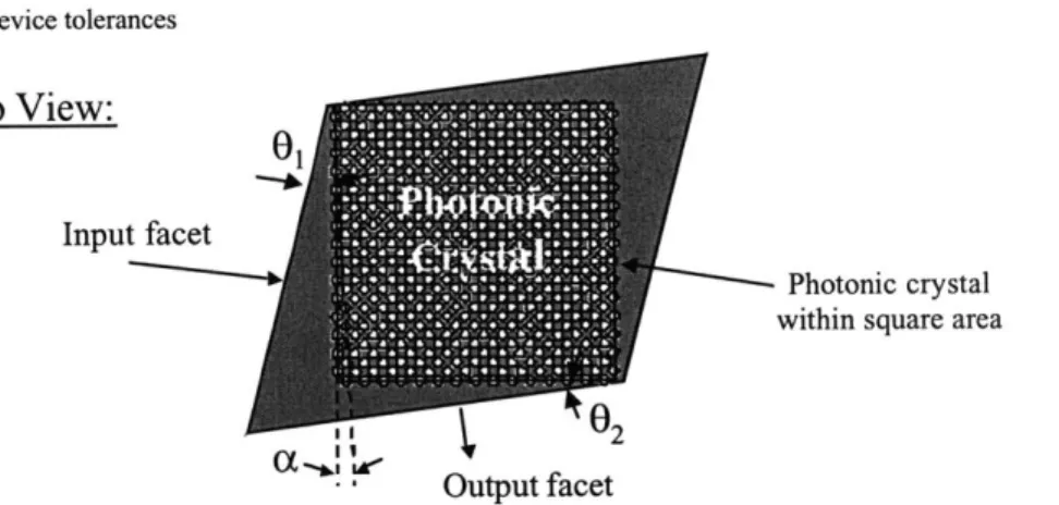
The top view of the design shown in Figure 2.10 shows how the GaAs region is shaped as a parallelogram with the photonic crystal occupying a square region within the parallelo-gram. The orientation of the parallelogram with respect to the photonic crystal edge is designed such that light entering the input facet at near normal incidence then exits the output facet at larger angles centered around the normal direction. The ideal performance
is designed such that an input angular sweep of approximately +/-20 will be amplified to
about +/-30' at the output for a wavelength of 3.1 ptm. A thick aluminum oxide (AlxOy) layer is used to minimize radiation loss into the GaAs substrate. The depth of the holes and the parallelogram sidewalls will be as deep as possible to facilitate coupling from an input
fiber.
Superprism device schematic (not to scale).
Top View:
FIGURE 2.10DESIGN THEORY & SIMULATION
To proceed with the design of our superprism, we calculated dispersion surfaces for sev-eral modes within a 2D photonic crystal consisting of air columns in GaAs. As discussed earlier in this chapter, the direction of wave propagation inside the photonic crystal is given by the direction of the group velocity (i.e. the direction normal to the dispersion sur-face). However, the direction of propagation as the beam exits the crystal is determined by the phase velocity due to the phase matching condition on the k-vector at the boundary. Therefore, for a photonic crystal superprism to have ultra-refractive effects that are pre-served at the output of the device, we must utilize regions of the dispersion surface that have highly sensitive phase velocity behavior. This is the key difference between our work and previous work thus far.
For the dielectric configuration shown in Figure 2.10, we have calculated the relevant dis-persion surface shown in Figure 2.11. The results are presented on a normalized basis. The computation assumes a finite slab thickness of 0.6a and a hole size of 0.4a. The indi-ces of refraction used were 3.4 and 1.5 for the GaAs and aluminum oxide layers respec-tively. This calculation is for guided modes with the magnetic field concentrated in the perpendicular polarization. The computed dispersion surface has a fairly flat region which is ideal for ultra-refraction.
FIGURE 2.11 Dispersion surface calculation for photonic crystal design. The square lattice orientation is shown in the inset [7]. I / I I I ' 0.6-0.4 -/O 0.2 / 0--0.2 --0.4- 0~ -. 6 7. 000
~
\X'/ I -0.8 -0.6 -04 -0.2 0 0.2 0.4 0.6 0.8 k, (2*pi/a)The method used to compute the dispersion surface in Figure 2.11 was as follows. The dispersion relation for guided modes propagating in a planar slab was computed using pre-conditioned conjugate gradient minimization of the Rayleigh quotient in a plane wave basis [6]. A numeric root-finder was used to solve for the exact wave vectors that corre-spond to a particular frequency. This computation was carried out for every orientation throughout the entire Brillouin Zone to map out the dispersion surface.
DESIGN THEORY & SIMULATION
The band structure for the superprism photonic crystal [7].
0.5-0.4 0.3 0.1 AN,
x
M
r
Explanation of Superprism ultra-refraction using the dispersion surfaces in the photonic crystal and GaAs [7].
Input Facet
Photonic Crystal Dispersion \Surface GaAs Dispersion -N Surface -0.8 -. 6 -0.4 -0.2 0 0.2 0.4 0.6 0.8 KxI (2pi/a) Group velocitydirection-Phase velocity direction
Output Facet
0.6 0.4 0.2 0 -0.2 -0-4 -0.6 ' ' | ' 1 NI I ' ' | I _T ' I 'Photonic Crystal / -,, ( Dispersion ) ( Surface Dispersion Surface-/k -0.8 -0.6 -0.4 -0.2 0 0.2 0.4 0.6 0.8 Kx (2pi/a)ki: Incident wavevector kf : Final wavevector
k
Y8OO
Design and Fabrication of a Superprism using 2D Photonic Crystals FIGURE 2.12 Q 0 C LL FIGURE 2.13 0.6 0.4 0.2 0 -0.2 -0.4 -0.6
-24DESIGN THEORY & SIMULATION
Figure 2.12 is the band structure for the superprism's photonic crystal. The computation uses the same assumptions as the dispersion surface calculation in Figure 2.11. The hori-zontal line represents an equi-frequency line at the normalized design frequency of 0.24. Our device operates by coupling to the lowest mode shown in this band structure. As stated earlier, we have assumed an input beam polarized such that the magnetic field is concentrated in the z direction. The lowest order mode corresponds to this polarization and is therefore the only mode that the input beam will couple to. Though the equi-frequency line intersects other higher modes, these modes correspond to other polarizations with the electric field concentrated in the z direction. In addition, the orientation of our photonic crystal is such that the beam is incident upon the GaAs/photonic crystal boundary at an angle and will only couple to the lowest order mode independent of polarization. This result is more clearly illustrated in Figure 2.13.
The ultra-refraction property of our superprism is illustrated in Figure 2.13. The boundary between the gallium arsenide and the photonic crystal lies along the F-M symmetry line of the square lattice. The two different arrows in Figure 2.13 represent k-vectors for two dif-ferent input beams which differ by only a small angle. As the beam propagates from GaAs into the photonic crystal, the phase matching condition on the tangential component of the k-vector must be met. The beam refracts into the photonic crystal as the k-vector moves from the GaAs dispersion surface to the photonic crystal dispersion surface.
The small difference between the two input wave vectors translates into a large change in the phase velocity inside the photonic crystal due to the flatness of the dispersion surface. As the two beams exit the photonic crystal at the output facet, the phase matching condi-tion is met again and the angle between the wave vectors is greatly magnified.
Figure 2.13 does not show the beams as they propagate from air to GaAs at the input and from GaAs to air at the output. However, the angular difference between the two beams will only be enhanced as the beams propagate into air. The result is a large angular sweep at the output for a very small angular sweep at the input. Similar considerations can also be used to realize frequency super-dispersion using a broadband source at a fixed angle of
incidence.
The photonic crystal dispersion surfaces shown in Figure 2.11 and Figure 2.13 corre-spond to the lowest order mode shown in the band structure in Figure 2.12. By traveling along a line of constant frequency on the band structure, we intersect points on the disper-sion surface corresponding to k-vectors in the directions of periodicity in the photonic crystal, which are the F-M and F-X directions for a square lattice. If there are multiple modes at a particular frequency, there are multiple dispersion surfaces.
Traveling along the equi-frequency line in Figure 2.12, we intersect both the lowest order mode, and two higher order modes. These two higher order modes have dispersion sur-faces shaped like circles with smaller radii. For near normal incidence, an input beam may be able to couple to these modes-though the coupling may be weak due to differences in polarization. However, we have designed the input facets such that the beam is incident
DESIGN THEORY & SIMULATION
upon the photonic crystal at steep angles as shown in Figure 2.13. At steep angles of inci-dence, the input k-vector will not be able to couple to these higher order modes because the phase matching condition cannot be met. Therefore, our beam will only couple to the lowest order mode in the band structure enabling us to concentrate more power in the mode of interest for our superprism.
Time domain simulation of superprism ultra-refraction. The simulation was performed on a simplified 2D structure which did not consider the effects of a finite device thickness [7].
Inpu
t0 T*.
Output ,
I
SInput Angle - 0 = -2*
Finite size effects
creates spherical
wave fronts
Al
//Input Angle -0 = +20
To demonstrate the experimental feasibility of our ideas we have carried out finite-differ-ence time-domain simulations on a simplified system. The simplified system has the same photonic crystal lattice structure as our device but is purely 2D (assumes infinite structure thickness) and is reduced in size. In the simulation, shown in Figure 2.14, a plane wave generated by a straight line of dipoles is launched into the GaAs region and propagates into the photonic crystal. The figures show snapshots of the z component of the magnetic field distribution.
Two Bloch waves are excited within the crystal. As they propagate, they are severely refracted. Upon exiting the photonic crystal, one of the Bloch waves is internally reflected
Design and Fabrication of a Superprism using 2D Photonic Crystals FIGURE 2.14
DESIGN THEORY & SIMULATION
at the GaAs/Air interface allowing a single Bloch wave to couple out into air. As the incoming beam is changed by +/-2*, the output beam sweeps through a large angular range of +/-300. In the high dielectric GaAs region, a fringe pattern can be observed due to inter-ference between the incident and reflected beams. The finite size of the simulation also causes the output beam to appear spherical. The arrows within the figures are just to guide the eye but demonstrate how the direction of the beam shifts with the slight change in the input angle.
RESEARCH APPROACH
3.0 RESEARCH APPROACH
3.1 Research Objective
Our goal is to design and fabricate a superprism device using a two dimensional photonic crystal in a gallium arsenide material system. The device will allow a small angular sweep at the input to translate into a large angular sweep at the output (i.e. ultra-refraction). In addition, an input beam with a small spread in frequencies will result in a large angular separation of these frequencies at the output (super-dispersion).
The superprism is composed of a two dimensional photonic crystal with a square lattice of air holes in gallium arsenide (see Figure 2.10). The photonic crystal rests on a thick layer of aluminum oxide on a gallium arsenide substrate. The depth of the air holes is as deep as possible. The feature sizes of the photonic crystal are scalable depending on the wave-length of operation. Our desired wavewave-length range of 2.8 to 3.8 ptm implies a lattice
con-stant of 672 to 912 nm, and a hole radius varying between 269 and 365 nm. The input and
output facets are air-GaAs boundaries positioned at specific design angles with respect to
the photonic crystal. The total thickness of the device (excluding substrate) is about 3.5
ptm while the top surface will have an area of about 2 cm x 2 cm.
The orientation of the parallelogram with respect to the photonic crystal edge is designed such that light entering the input facet at near normal incidence, then exits the output facet
at magnified angles centered around the normal direction. The ideal performance is
designed such that an input angular sweep of approximately +/- 2' will be amplified to about +/- 300 at the output for a wavelength of 3.1 jpm.
3.2 Design Tolerances
In order to identify the steps necessary to fabricate the superprism, we needed to deter-mine a number of tolerances on the device design. The results are presented in Figure 3.1.
Changing the ratio of hole size to lattice constant (r/a) changes the frequency at which the
dispersion surface is flat thereby shifting the frequency at which we will observe our
per-formance specifications. By simulating a change in r/a from 0.40 to 0.35 and
recalculat-ing the dispersion surface, we found that the frequency at which the dispersion surface
was now flat (the performance frequency) decreased by about 7%. An error in r/a by
-0.05 would shift our performance frequency from 3.1 ptm to 2.9 pm which is acceptable
from a testing perspective. We therefore aim to stay within this error of 7% or r = 300 nm
+/- 38 nm. However, since the hole size is susceptible to a number of sources of variation
from the lithography as well as etching steps, this parameter is anticipated to be the most difficult parameter to meet.
Lattice squareness refers to the degree to which the grid of holes in the photonic crystal is actually square. Errors in the squareness of the grid may be introduced in the fabrication
Design and Fabrication of a Superprism using 2D Photonic Crystals 28
RESEARCH APPROACH
process due to the need for two exposures when patterning holes using interference lithog-raphy. Small errors of this type would again alter the frequency at which the dispersion surface is flat because the periodicity in hole spacing would be altered. By simulating an error of 100 in the distortion of the square grid, we found that the performance frequency increased by about 7% from 3.1
stm
to 3.3 tm. To keep the error below1%,
we aim for a tolerance of +/-1'. Please see Section 4.3 for a discussion of how this tolerance is met.FIGURE 3.1 Superprism device tolerances
Top View:
01
Input facet
Photonic crystal within square area
Output facet
1) radius of holes: r = (0.40 +/- 0.05)*a where a is the lattice constant => r=300+/-38 nm 2) lattice squareness: the angle between two lattice vectors = 90 +/- 10
3) alignment of square shape to parallelogram:
01=38
+/- 10, 02=11+/- 104) alignment of lattice edge to square edge: the angle a between a line of holes and the
square edge a = 0.0 +/- 0.50
As stated above, the angled facets of the device allow light entering the input facet at near normal incidence to then exit the output facet at larger angles centered around its normal direction. Small errors in these angled facets with respect to the boundary of the photonic crystal would shift the input/output wavevector angles to directions which are not centered about the normal. This error would not otherwise effect the performance of the device. We therefore aim for a tolerance of +/- 10 on this specification.
The use of interference lithography to pattern the large area of photonic crystal holes may introduce errors in the alignment of the hole lattice to the edge of the square region. Ide-ally, the edge of the square area should be completely parallel to a line of holes of the pho-tonic crystal so that
a
= 00 (as shown in Figure 3.1). A non-zeroa
will rotate the dispersion surface with respect to the GaAs-photonic crystal boundary. We have designed the device such that a +/- 20 input swing will result in an output swing of +/- 300. Errors which rotate the dispersion surface would change this input/output angular magnification performance because we would be utilizing a different part of the dispersion surface. Through simulations, we have estimated that ana
= 10 error in boundary alignment wouldRESEARCH APPROACH
change our design performance in two ways depending on whether
a
is positive ornega-tive: a +/- 1.50 input translating to +/- 300 output, or +/- 2.50 input translating to +/- 30* output. We therefore set our tolerance on this alignment specification to
a
= 0 +/- 0.50. 3.3 Fabrication SequenceThe following is a general outline of the steps necessary for the successful fabrication of the GaAs superprism considering the tolerances discussed in Section 3.2. Please refer to Chapter 4 for detailed discussion and results relating to each of the fabrication steps.
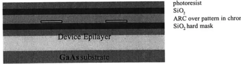
FIGURE 3.2 Growth of epilayer, sputtering of SiQ2 and Cr evaporation
Growth of device epilayer using molecular beam epitaxy: 450nm GaAs, 3000nm AlAs on GaAs substrate
450nm GaAs
3000nm AlAs Device Epilayer
- Substrate coated with 300nm SiO2, 5Onm chrome
50nm Cr
300nm SiO2
The device epilayer which consists of 450 nm GaAs and 3000 nm AlAs on a GaAs sub-strate is grown using molecular beam epitaxy. A 300 nm layer of Si0 2 is sputtered using the sputtering system in the Nanostructures Laboratory (NSL). This Si02 layer will be used as a hard mask for etching the GaAs/AlAs epilayer. A 50 nm chrome layer is depos-ited using an evaporator. This layer will be used to define the parallelogram and square shape of the device.
Figure 3.3 is a general schematic of the photolithography mask patterns used to define the device shape. Please see Chapter 4 for more detailed discussion. Two photolithography steps will be used: the first using Mask
1
will allow for the exposure of holes within the square area of the device, and the second step using Mask 2 will protect the square area as the unwanted holes outside the parallelogram are etched away. An alignment grid on Mask1
aids in the alignment of the holes to the device shape. Alignment crosses on Mask1
and alignment dots on Mask 2 aid in the alignment of the two patterns to each other.Design and Fabrication of a Superprism using 2D Photonic Crystals
RESEARCH APPROACH
Photolithography mask design schematic. Mask I and Mask 2 are two 4" masks with the chrome pattern on glass (mask outline not shown).
Mask
1-+. +----Mask 2
+
Each device
20x2Omm ' 0/2" wafer outline
(not on mask)Photolithography with Mask 1
- use Mask 1 to expose/develop square and parallelogram in photoresist with alignment marks and alignment gratings
Photoresist pattern
- Wet etch chrome (CR7 etchant); acetone/ash
photoresist
Chrome pattern
Pattern on wafer:
The first photolithography mask is used to contact expose the parallelogram and square shapes in photoresist as shown in Figure 3.4. This mask exposes cross-shaped alignment marks which are used to align this pattern to the pattern later exposed using Mask 2. The square area in the middle of the wafer is a grid which is used to align the Interference
Design and Fabrication of a Superprism using 2D Photonic Crystals FIGURE 3.3 0 / I * -.4 FIGURE 3.4 31
RESEARCH APPROACH
Lithography exposure to this Mask 1 pattern. A wet etch is used to transfer the resist pat-tern to the chrome layer.
FIGURE 3.5 Interference Lithography with use of trilayer resist stack. Please see Chapter 4 for a discussion of thicknesses. " Spin trilayer: thick Anti-reflective coating (ARC), thick SiO2 interlayer, photoresist
photoresist SiO2
ARC over pattern in chrome SiO2hard mask
- Expose/develop holes in photoresist using interference lithography (IL) - use mask 1 grid to align hole pattern to device shape
Holes in photoresist SiO2interlayer
ARC over pattern in chrome
Sio2hard mask
Figure 3.5 shows the preparation of the substrate and the subsequent Interference Lithog-raphy exposure. Interference lithogLithog-raphy is used to pattern the whole wafer with holes. The trilayer resist stack consisting of: photoresist, SiO2 interlayer, and anti-reflective coat-ing (ARC) is used to minimize reflections off the substrate durcoat-ing the exposure and facili-tate pattern transfer to the SiO2 hard mask layer. Please see Chapter 4 for a discussion of the relevant thicknesses. The alignment grid on the wafer is used to align the hole pattern to the device shape in chrome.
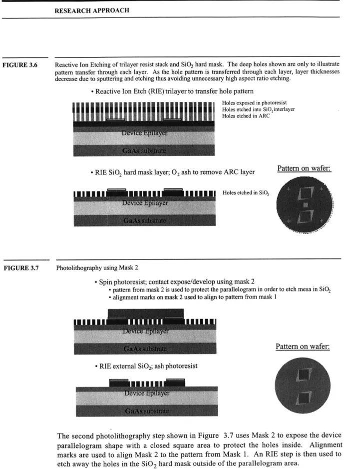
Figure 3.6 shows the transfer of the hole pattern to the SiO2 hard mask layer using Reac-tive Ion Etching (RIE). The gases used to etch the SiO2 and ARC layers are CHF3, and He/02 respectively. A CHF3 RIE step is then used to transfer the pattern into the SiO2 hard mask layer. The chrome layer will prevent the etching of holes outside the square area within the parallelogram shape as shown by the pattern on the wafer in Figure 3.6. A He/0 2ash step is used to remove any remaining ARC.
Design and Fabrication of a Superprism using 2D Photonic Crystals 32
RESEARCH APPROACH
Reactive Ion Etching of trilayer resist stack and SiO2 hard mask. The deep holes shown are only to illustrate pattern transfer through each layer. As the hole pattern is transferred through each layer, layer thicknesses decrease due to sputtering and etching thus avoiding unnecessary high aspect ratio etching.
Reactive Ion Etch (RIE) trilayer to transfer hole pattern
I****i
I II
miii|Holes
exposed in photoresistHoles etched into SiO2interlayer
Holes etched in ARC
- RIE SiO2 hard mask layer; 02 ash to remove ARC layer
jg§1 111§1
gg
M i* gf
Holes etched in SiO2Pattern on wafer:
FIGURE 3.7 Photolithography using Mask 2
Spin photoresist; contact expose/develop using mask 2
- pattern from mask 2 is used to protect the parallelogram in order to etch mesa in SiO2 - alignment marks on mask 2 used to align to pattern from mask I
Pattern on wafer: -RIE external SiO2; ash photoresist
The second photolithography step shown in Figure 3.7 uses Mask 2 to expose the device parallelogram shape with a closed square area to protect the holes inside. Alignment marks are used to align Mask 2 to the pattern from Mask 1. An RIE step is then used to etch away the holes in the SiO2hard mask outside of the parallelogram area.
Design and Fabrication of a Superprism using 2D Photonic Crystals FIGURE 3.6
RESEARCH APPROACH
Reactive ion etch substrate and oxidize AlAs layer
RIE epilayer using BC13; Cr layer will also be etched
SiO2 hard mask GaAs
AlAs
- Remove SiO2
- Lap the substrate and cleave the wafer * Wet oxidize the AlAs layer to become A1kOY
Pattern on wafer:
GaAs AO Y
A final RIE step using BCl3 shown in Figure 3.8 transfers the hole pattern and the device shape into the GaAs/AlAs epilayer. Any remaining SiO2 is removed using CHF3 RIE. The substrate is thinned through lapping and we then cleave the wafer to separate the indi-vidual devices. The last step is a wet oxidation of the AlAs layer creating our low index
AlXOy layer.
All fabrication steps are performed in laboratories at the Massachusetts Institute of Tech-nology. The GaAs/AlAs epilayer is grown in the Chemical Beam Epitaxy Laboratory, most processing, including lithography and reactive ion etching, is performed in the Nano-structures Laboratory, and the die sawing is performed in the Microsystems Technology Laboratory.
Testing of the device will be performed in collaboration with Rockwell Science Corp.
Design and Fabrication of a Superprism using 2D Photonic Crystals FIGURE 3.8
DISCUSSION & RESULTS
4.0
4.1
Design and Fabrication of a Superprism using 2D Photonic Crystals
DISCUSSION & RESULTS
Molecular Beam Epitaxy Results
The GaAs heterostructure shown in Figure 4.1 was grown using the Riber Instruments gas source molecular beam epitaxy (GSMBE) system in the Chemical Beam Epitaxy group at MIT. The structure was grown successfully with the following layers:
* 400 nm GaAs * 50 nm Al0 50GaO. 5As
e 3000 nm AlAs
o 50 nm Al0.50Ga0.50As * GaAs substrate
The 50nm AlGaAs layers are intermediary layers which are helpful during the oxidation step for stabilizing the GaAs interface. Please see Section 4.6 for discussion of these results. This intermediary layer will not oxidize and will therefore serve as a high index layer for guiding light. With this in mind, the top GaAs layer was grown to be 400 nm so that the total high index layer thickness was 450 nm.
A scanning electron microscope (SEM) image of a randomly fractured edge of the GaAs heterostructure
showing the GaAs/AlGaAs/AlAs epilayer on the GaAs substrate. The 50nm AlGaAs layers are not clearly visible due to the non uniformity of the surface.
FIGURE 4.1
DISCUSSION & RESULTS
Photolithography Results
As outlined in Section 3.3, photolithography will be used to define the superprism device shape. Two photolithography steps will be used with the mask designs shown in Figure
4.2: the first using Mask 1 and the second using Mask 2.
Photolithography mask designs: Mask 1 (left) and Mask 2 (right). 2" Wafer outline and cross-hairs are for reference and will not be exposed. Cross and circle-shaped alignment marks are used to align the patterns from Mask 2 to the pattern exposed on the wafer using Mask 1.
Outpu Facet Input Facet
Mask 1
7
S ~1 N.~ N N 'N/
/ .'~ /I N. N.Mask 2
The device shape defined by the above masks differs from the shape shown in the design schematic shown in Figure 2.10. The inputs and outputs of the devices are still defined by angled facets. However, in order to optimize the number of devices per wafer, the corners of the original parallelogram shape have been trimmed. Trimming these corners allows us to pattern four device shapes per 2 inch wafer. However, the number of devices per wafer is actually eight due to the fact that each device shape has two input and two output facets on opposite sides of the photonic crystal area. Trimming the corners also helps us during the oxidation step by decreasing the lateral distance that the oxidation front needs to travel.
Mask
1
defines the device shape with an open square area. The middle of the wafer pat-tern has an alignment grid with a period of about1
micron to allow for alignment of the hole pattern to the device shape during the Interference Lithography exposure step. Mask 2 covers the whole device area so that the holes exposed outside the device area can be etched away while the holes inside the device are protected. See Section 3.3 for details of these fabrication steps. Cross and circle-shaped alignment marks are used to align the pat-terns from Mask 2 to the pattern exposed on the wafer using Mask 1.Design and Fabrication of a Superprism using 2D Photonic Crystals 4.2
FIGURE 4.2
DISCUSSION & RESULTS
4.3 Interference Lithography Results
Interference lithography is used to pattern the square lattice of holes for the 2D photonic crystal. Interference lithography is a more appropriate lithography technique for this superprism design than photolithography or electron beam lithography because the hole pattern is periodic, covering a
large area, and with minimum feature sizes under hIm.
4.3.1 Basic Overview of Interference Lithography
Interference lithography (IL) allows patterning of periodic structures over a large area. The periodic pattern is formed by the constructive and destructive interference of light waves which form a standing wave at the substrate surface. This standing wave exposes a grating pattern on the substrate as illustrated in Figure 4.3.
FIGURE 4.3 In interference lithography, the standing wave formed by the interference of two light beams exposes a periodic grating on the substrate. In this schematic, the incoming waves are approximated as plane waves when in reality they are spherical.
P
The period of the grating (P) depends on the source wavelength (k) and the half-angle between the two beams (0) according to:
P = (EQ 4.6)
2 sinO
Two IL systems in the Nanostructures Laboratory (NSL) at MIT were investigated for pat-terning the photonic crystal used in this thesis: the Lloyd's mirror interferometer, and the two-beam interferometer.


![FIGURE 2.11 Dispersion surface calculation for photonic crystal design. The square lattice orientation is shown in the inset [7]](https://thumb-eu.123doks.com/thumbv2/123doknet/14679419.558856/23.918.279.708.582.896/figure-dispersion-surface-calculation-photonic-crystal-lattice-orientation.webp)