Design of a Four-Phase Switchmode High
Efficiency Power Supply
by
John Mburu Gachora
Submitted to the Department of Electrical Engineering and
Computer Science
in partial fulfillment of the requirements for the degrees of
Master of Engineering
and
Bachelor of Science in Electrical Engineering and Computer Science
at the
MASSACHUSETTS INSTITUTE OF TECHNOLOGY
May 1994
( Massachusetts Institute of Technology 1994. All rights reserved.
Author
... .-
-...
Department of Electrical Engineering and Computer Science
May 16, 1994
Certified
by...
le\,
Accepted by.
Chairman,
..--. .·.· .·.W·T. ·.Martin F. Schlecht
rofessor
Electrical Engineering
C oesso
}
IA Thesis Supervisor
r
\
Frederic R.Morgenthaler
Departmental Committee on Graduate Students
Design of a Four-Phase Switchmode High Efficiency Power
Supply
by
John Mburu Gachora
Submitted to the Department of Electrical Engineering and Computer Science on May 16, 1994, in partial fulfillment of the
requirements for the degrees of Master of Engineering
and
Bachelor of Science in Electrical Engineering and Computer Science
Abstract
In this thesis, a four-phase switchmode dc-dc converter has been designed. The con-verter uses a two stage topology whose advantages over the single stage topology have been outlined. Paralleling of converters as a means for better perfomance has been investigated. Specifically effects of interleaving on output voltage ripple has been discussed. The choice of topology and components makes the design a possible standard for future designs, as well as a good candidate for converter fabrication. Special multi-phase magnetic structures which use flux cancellation methods to sup-port multiple coils have been used for the inductance and the transformer. Results of tests on the prototype are presented.
Thesis Supervisor: Martin F. Schlecht Title: Professor of Electrical Engineering
Acknowledgments
Foremost, I would like to extend my special thanks to Prof. Martin Schlecht, my thesis supervisor for his guidance and unending inspiration. I am forever indebted to him for having given me the opportunity to apply much of what I have learned at MIT.
Thanks to David Otten for the immense help in getting this work started. I thank him for the work he had done previously from which I borrowed heavily.
I would also like to thank Beth McDonald, Vivian Mizuno and Anne Hunter for their continued support and good cheer throughout this work.
Thanks to members of the CAES Advanced Study Program staff, Dr Paul Brown, Debbie, Bev, Susan, Diane, and Margaret for all your good cheer and encouragement. Paul, thanks for everything.
Thanks to the members of the Lab for Electromagnetic and Electronic Systems for their assistance and guidance. In particular, thanks to Dave Perrault, Kwabena Ofori, Mary Tolikas, Jeff Chapman, Robert Selders, Ahmed Mitwalli, Christine Odero, Prof. Steve Leeb, and Prof. Steve Umans.
To my dear parents, Wanjiku and Gachora Wamithi: Nindamucokeria ngatho muno ni wendo wanyu na mahoya maingi. Mwathani amurathime muno na muture matuku maingi. Tiga ni inyui ndingikinyite haria ndi..
To my siblings, Wanjiru, Wamithi, Thandi, Waweru, Hannah, Njeri, Maria, Wair-imu, Njoki, Karanja, Kamau and Wangari (Mekacy),and all your families thank you for all your emotional support in good and bad times.
Thanks to Jane Wahome for being there when I needed her.
Thanks to all my friends and loved ones: Dedan Kimotho, Safroadu Yeboah-Amankwah, Dennis Ouma, Peter Orondo, Anne Wamunyu, the Sang'udis, the Kasham-buzis (mama, thank you!), Peju, Dudzai, ATF staff, and the whole African fraternity.
Contents
1 Introduction
1.1 Overview . ... 1.2 Two-Stage Converters ...
2 Design Considerations of the Pre-Regulator
2.1 The Pre-regulator Stage: Down-Converter . . 2.1.1 DC-DC down converters ...
2.1.2 The Conversion Ratio ...
2.1.3 The Down Converter Implemented . . 2.1.4 Determining Design Values . .
2.2 Issues in Paralleling Converters ... 2.2.1 Interleaving ...
2.2.2 Layout. ...
3 The Isolation Stage and Output Filter
3.1 Push-pull Converters ... 3.1.1 Operation.
3.2 Design of the Isolation Stage ... 3.2.1 Topology . ...
3.2.2 Design Considerations and Discussion . 3.2.3 Losses and Energy Recovery ...
3.3 The Output Stage. ...
4 The Control: Putting it all Together
9 9 11 14 14 15 17 18 22 24 24 25 28 28 28 31 31 33 35 37 38 . . . .: :
...
...
...
...
...
...
...
...
...
...
...
...
...
...
...
4.1 Types of Drivers Required .... 4.1.1 High-Side Driver . . 4.1.2 Low-Side Driver .
4.2 Drive Signals and Implementation
4.2.1 Drive Signals . . . . .
4.2.2 Implementation ...
5 Testing and Experimental Results
5.1 Testing the The Down Converter ... 5.1.1 Experimental Results.
5.2 The Isolation Stage ...
5.2.1 Experimental Results . . . .
5.2.2 Waveforms from Push-Pull stage
5.3 Other Concerns ...
5.3.1 Temperature Considerations .... 5.3.2 Cost analysis ...
5.3.3 Power Losses . . . .
6 Conclusions and Further Research
6.1 Conclusion. ... 6.2 Further Research.
A P-Material used for Ferrite Core Design
B PCB Layout 38 38 41 42 42 44 46 47 47 52 52 53 56 56 56 57 58 58 59 60 62
...
...
...
...
...
...
. . . . . . . . . . . . . . . . . . . . . . . . . . . . . . . . . . . . . . . . . . . . . . . . . . . . . . . . . . . . . . . . . . . .List of Figures
1-1 Single stage converter block diagram ... 12
1-2 Two stage converter block diagram ... 12
2-1 The most common down-converter ... 15
2-2 Ideal inductor current ... 17
2-3 The converters connected in parallel ... 19
2-4 The down-converter analyzed below ... 20
2-5 Inductor Current for an ideal case ... . 21
2-6 Effective inductor implemented ... .. 24
2-7 Multi-phase structure used to build the parallel converter inductance 26 2-8 Cross-section of the inductor windings ... 27
3-1 Basic push-pull stage ... 29
3-2 Resulting curve of transformer primary voltage ... 30
3-3 Resulting transformer primary current ... 30
3-4 Topology of Push-pull stage designed ... 32
3-5 The multi-phase magnetic transformer core ... 33
3-6 Cross-section of the transformer stage ... 34
3-7 One branch of the Push-pull showing the energy recovery circuit.... 36
4-1 The complete path of current through the circuit. ... 39
4-2 Suggested driver unit for the high-side switches ... 40
4-3 Clock implementation: make R1 > R2 ... 42
4-5 The Control Circuit: a detailed diagram ... 45 5-1 Snapshot showing the input voltage, output voltage, and switch drive
signal ... 48 5-2 Input-Output voltage relationship for a single down converter ... 49 5-3 Relationship between output ripple and input voltage for a single down
converter ... 50 5-4 Picture showing a set of measurements taken for two down converters
operated out of phase. ... 51 5-5 Drive signals, Vgs, for the two pairs of MOSFETs used ... 53 5-6 Drain Voltage and Input bus voltage (switching effects). ... 54 5-7 Drain-Source voltage and the Output Voltage (Switching effects on
output voltage ripple). ... 54 5-8 Voltage across one primary coil and the resulting waveform across
sec-ondary coil ... 55 B-1 Top PCB layer showing first set of transformer primary windings and
inductor windings ... 63 B-2 Second PCB layer showing secondary transformer winding ... 63 B-3 Third PCB layer showing secondary transformer windings ... 64 B-4 Bottom PCB layer showing second set of primary transformer windings 64
List of Tables
5.1 Table of Results for a Single Down Converter. ... 48 5.2 Table of Results for Two Down Converters Operated out of Phase... 51 5.3 Summary of the estimated bulk (in thousands) cost of materials for
the converter. ... 56
Chapter 1
Introduction
1.1
Overview
The need is growing for denser, lighter and more reliable power supplies as the idea of point-of-load converters becomes more important. Power supplies have not kept up with the pace for miniaturization of electronic equipment. In the aerospace and automotive industry where minimizing weight improves performance and lowers man-ufacturing and operating costs, lighter power supplies that perform just as well or better than existing ones would have considerable advantage in the market. In the computer industry where size and portability are becoming critical, smaller power supplies will be necessary to allow for miniature laptops as well as desktops.
Further, smaller power supplies may allow for standardization that will help reduce the practice of designing a power supply for every new application. New converter designs may allow automation of the whole production process eliminating the neces-sity for hand assembly which is both slow and error-prone. Conditions in the power industry have called for point-of-load converters that will deliver power straight from the supply lines and that are capable of operating from any supply line (11OV, 220V Or 240V). This will set a global standard which will make power distribution systems transparent to equipment and system designers.
Most of today's power supplies operate at efficiencies in the 80% to 85% range; which for a 10OW supply translates to a heat dissipation of 15 to 20 Watts. A
substantial cost of the power supply, in space, material and manufaturability goes into getting rid of this heat. In most cases, an electrically isolated heat sink is attached to the circuit board on which the power supply components rest. This not only adds cost in terms of space and material, but it also requires far more hand
manipulation, rendering the product to greater opportunity for loss of quality.
The physical limit of power supplies lies largely in the sizes of the components used. Different power supply topologies are used by different manufacturers, but the underlying methods of construction are generally the same. Whereas there may be some improvements in the physical designs of the components in the future, new power supply topologies will not be much different from what we already have today. If any substantial improvement is to be made in the area of power supply design and construction, the problems outlined above must be addressed. In particular, real improvements will come from changes in manufacturability. New heat-removal mechanisms must be found to ease the complexity of fastening heat sinks to the product. All this calls for new design and construction standards.
This thesis is a report of work done to design and construct a power supply that will set some of the standards called for above. The design uses a two-stage topology that aims to distribute the dissipation among many components so that each component can stay sufficiently cool to eliminate the need for extra heat sinking. To allow for industrial automated fabrication surface mount technology has been used for all the required components. The power supply built uses a combination of a down-converter and a modified push-pull isolation stage to achieve power transformation from 90OVdc to 5Vdc. The power supply constructed had the following specifications:
* Delivered Power =100W
* Operating frequency = 250kHz
* DC input voltage = 36-72V
*
DC output voltage = 5V* Output ripple below 100mV * Efficiency above 87%
* Miniature board size (2.5in by 1.75in by 0.3in)
Further considerations were made to allow for simple component adaptation for the power supply to operate at a higher input line voltage as is required in most other countries. Although the power supply presented here was aimed to meet the specifications above, same-size components are available to enable the product to operate in 70-400V input voltage range.
1.2 Two-Stage Converters
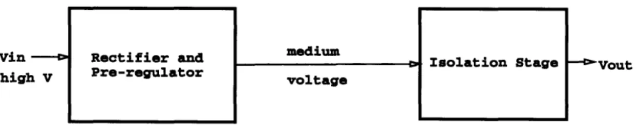
The most straightforward dc-dc converters are made of a single conversion stage, usually the isolation stage, as shown in Fig. 1-1 and are commonly referred to as single-stage converters. Front-end converters are usually built this way using pulse width modulation controlled bridges. This design has the great advantage of design simplicity and low cost of implementation. One of its main shortcomings, however, is that it displays switching losses that increase drastically with increase in frequency. At the same time the step-down stage has to maintain a constant output voltage over a wide range of input voltage range, (typically 3:1). For a down-converter, this comprises its efficiency.
The converter designed in this thesis is a two stage design, shown in Fig. 1-2. This has two converters in series. As a result it requires more parts and a more complex control mechanism than a single stage converter. The particular topology described in this thesis has a down-converter stage in series with a push-pull transformer isolated stage. The down converter stage provides line regulation and is hereafter referred to as the pre-regulator while the push-pull provides isolation between the input and the output and is hereafter referred to as the isolation stage.
In his thesis, Andrew Ferencz1 has outlined the advantages that two-stage con-1A 250 W High Density Point-of-Load Converter, Andrew Ferencz, Masters Thesis, 1989
high voltage
dc
Vout
5V, 12V
Figure 1-1: Single stage converter block diagram
medium
voltage
Figure 1-2: Two stage converter block diagram
Vin Conversion stage with Duty-ratio Control vin -high V Rectifier and
verters have over single-stage converters:
* Two stage converters allow for the use of smaller devices in terms of current and voltage rating. Generally, electrical devices such as transformers, MOSFETs, and diodes exhibit losses that are proportional to their capacity ratings. Hence, per device losses are reduced when two stage converters are used. If a single stage is used, the duty ratio (or the turns ratio in case of transformer) would have to be a lot bigger for the same transformation to occur. For example, consider in our case an input voltage range of 36-72V to be transformed in to a 5V output value. If a single push-pull stage is used with the same design used on the topology shown, we would require a turns ratio of about 9:1. Since the voltage across the transformer would be about constant, the MOSFETs would have to be driven at a high frequency, and they themselves would have to be a rating higher than 180V. This means they would experience much higher stress and consequently higher switching losses. When these switching losses, the device on-resistance losses, and the transformer turns resistance and inductive losses are factored in, the two stage topology displays a higher overall efficiency. * A higher frequency also allows for the use of smaller components, in terms of
capacitive and inductive effects.
* A two stage converter also allows for a less sensitive control.
Because of the fact that two-stage converters may require more switches, more storage components, and more complicated control circuitry than a single-stage con-verter, a designer might only want to consider using a two-stage design if the power level is large (over 100W) or transient performance is important. The power handling capability of a commercial power supply corresponds roughly to the cost of the power supply which is on the order of one dollar per watt. A full-bridge converter which has four primary side switches is used for power levels above 250W. A working two-stage converter has just as many switches (four).
Chapter 2
Design Considerations of the
Pre-Regulator
This chapter describes the design of the pre-regulator stage. Details of the choice of components and specifications is presented.
2.1 The Pre-regulator Stage: Down-Converter
The pre-regulation serves the purpose of setting the voltage level across the isolation transformer stage. Since the input voltage is relatively high, a high turns ratio would be required for the transformer; but the presence of the pre-regulator enables us to set the voltage across the transformer to as low a value as desired. In this case, the input voltage ranges between 36V and 72V, and the voltage across the transformer is 30V. This value of transformer voltage is chosen arbitrarily, the desire being to make it as large as possible but appreciably less than the minimum operating voltage of 36V. A series connection of transformer blocks allows us to divide this 30V into two transformer primary voltages of 15V each. This in turn necessitates a turns ratio of
3:1 for a 5V output level.
The pre-regulator consists of four 250kHz, 28W discontinuous mode down con-verters in parallel operated 900 out of phase (ripple frequency at 1.0 MHz) that form the ground-reference for transformer stage. The pre-regulator is designed to operate
at an upper voltage level of 60V.
2.1.1
DC-DC down converters
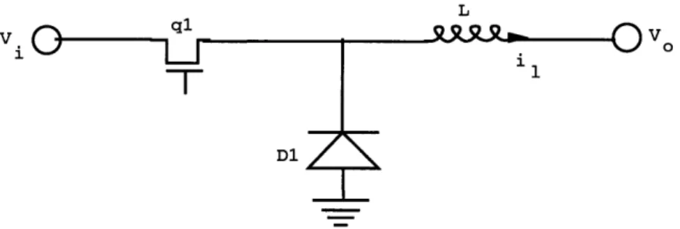
Fig. 2-1 shows the basic topology for an down converter. We assume that the converter components are lossless (in actuality, these components possess resistive properties and are therefore quite lossy). The operation of the converter is represented by the switching function q(t), which is 1 when the transistor is on, and 0 otherwise.
L
V
i
VoFigure 2-1: The most common down-converter
For a continuous mode operation, the converter goes through two states of
oper-ation. In the first state (charging state), the transistor is turned on, i.e., q(t) = 1.
The diode is reverse biased and is forced off. The input voltage Vin begins to charge up the inductor linearly, and at a rate proportional to the inductance value. This charge reaches a maximum level that is determined by the duty-ratio; the duty-ratio is defined as the fraction of the period for which q(t) = 1.
When the transistor is turned off, the inductor current forward-biases the diode
forcing the inductor's stored energy to be transfered to the load. This setup has the advantage in that the load is driven with current rather that voltage.
In the discontinuous operation, the converter goes through three states. For a fraction of the period D, the transistor is on and energy is transferred form the
source to the inductor as described above. When the transistor is turned off, the inductor discharged for a section of the period D1. By the end of the section D1, the
inductor has fully discharged, and both the transistor and the diode are essentially off. This is called the dead-time of the system during which time the inductor current
is zero.
Note that the difference between a continuous-mode (CCM) and a discontinuous mode converter (DCM) is the value of the inductance. The CCM has a larger induc-tance than the DCM. Thus the DCM has faster dynamics than the CCM. At the start of every cycle, the DCM converter has delivered all its energy to the next stage. This allows the DCM converter to respond to a transient output current or input voltage in one period with an instant change in duty-cycle ( though with a small change in output voltage) while the CCM version must accumulate volt-seconds on the inductor over many cycles to change its output current.
In the CCM converter, an increase in load current requires an increase in the DC current in the inductor. Thus, the positive voltage on the inductor must remain on longer to add net positive volt-seconds across the inductor. This results in a temporary decrease in the current delivered to the load, because the average time the rectifier conducts is decreased. This reaction demonstrates the presence of a right-hand-plane zero which makes control difficult. A DCM converter has no zeros; thus it is easier to control.
A DCM converter is favored more for buck-boost converters because it is not only easier to control but also it has a faster response, and it requires less magnetic energy storage. The large current ripple provides a larger signal for providing a current-mode
control. Since the transistor is turned on with zero current in the inductor, the
turn-on loss is reduced to turn-only a capacitive energy discharge. Zero initial inductor current also allows for a slow turn on of the switch which reduces the current spike from the charging of the MOSFET gate. This spike might otherwise trigger any current mode comparator in the circuit.
The DCM converter however has its disadvantages. It requires more capacitance for filtering because it has a larger current ripple. It has higher conduction losses
because the rms current is larger than that of the CCM converter. It displays larger turn off losses because the peak current is larger ( about twice as large as that of the CCM at turn off).
2.1.2 The Conversion Ratio
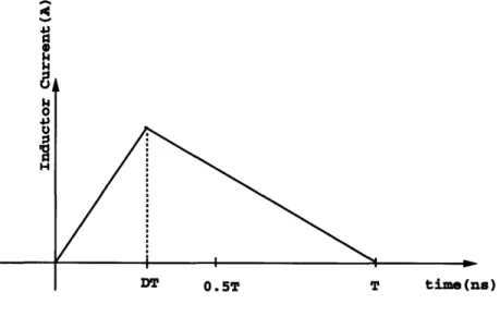
Consider the case when the converter in Fig. 2-1 is operated in the discontinuous mode. The ideal linearized inductor current has the shape shown in Fig. 2-2. Let
the duty-ratio be D, and the fraction of the period it takes to discharge the inductor
be D1 During the time when q(t) = 1, (the time DT) the inductor will charge up
according to the equation:
4c S UP 0 U 140 4J 0 :j 10
Inductor Current in DCM operation
D*T T time(s)
Figure 2-2: Ideal inductor current
Vi - VAt (2.1)
L
The inductor will charge up to a maximum value of:
V-Vo
il,peak = V DT (2.2)
When the
transitor is turned off and the diode forward-biased, the inductor will When the transitor is turned off and the diode forward-biased, the inductor will
discharge as in:
- V"At
Ail = V (2.3)
This linear discharge will continue until il = 0, at time D1T. During the remaining
part of the period, the inductor current is zero. To develop the relationship between the input voltage and the output voltage, let us consider the steady state operation of the system described above. Since the inductor is assumed to be lossless, the average voltage across the inductor must be zero.
(Vi-V)D + (-V)D
1= 0
D
Vo = D Vi
D+D
1where Vi, Vo are the average input and average output voltages respectfully.
When the system is operated at maximum power transfer, the value of D1 is set
to 1 - D. This operation is right at the edge of the continuous mode operation. At
this point the output voltage is related to the input voltage through Vo = DVi. Thus
the output voltage will always be less (or equal if D=1) to the input voltage; hence
the term down-converter.
2.1.3
The Down Converter Implemented
The actual converter used in the system constructed was a modified version of con-verter described above. Instead of the direct connection of the concon-verter to the input voltage, the converter is connected from the ground point of the push-pull isolation stage. The idea is to allow the use of N-channel devices for switching. P-channel de-vices have a higher on resistance than N-channel dede-vices and carry higher gate-source capacitance. This makes them not only more lossy, but also more difficult to remove charge from the gate at turn-off.
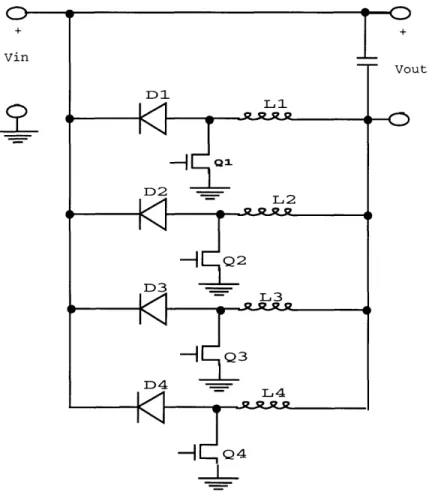
Four similar 250 kHz, 28 Watt discontinuous mode down converters are connected in parallel and operated 90° out of phase as shown in Fig. 2-3. The down converters
ib~ - - -7~~+ D1
Li
D2 - L25
Q2
D3-I
Q3
4 4t[-"13
Vout ; 0-- Q4
Figure 2-3: The converters connected in parallel
+
Vin
I'
In order to design the converter, the operation of the DCM needs to be calculated. The equations used to determine the design are developed next.
Observe that the operation of this type of converter is the equivalent to the oper-ation of the down converter discussed above. Its operoper-ation is defined by the following development.
Figure 2-4: The down-converter analyzed below
The analysis below refers to Fig. 2-4. During the interval when the transistor is
on, DT;
VL = Vin - Vout
During the interval (1 - D)T when the switch is off;
VL = -Vout
The average voltage across the inductor is 0:
D(in - vout) + (1- D)(-out) =
Vout = Dvin
This shows that this converter is equivalent to the one shown in Fig. 2-1. The peak inductor current will be determined as the integral of the voltage drop with respect to time:
iL f L dt
IL,peak = Vi - Vot DT
L
For a DCM operation, iL drops to 0 during the period (1 - D)T. At the edge of
DCM operation (right before we cross over to CCM) this implies:
-pel - t Vou
,peak in VoutDT = ut(1 -
D)T
L L
which is basically another derivation of the relationship between vi, and vt.
W 0 46) U i H DT 0. 5T Sa)
Figure 2-5: Inductor Current for an ideal case
Note that this result is exactly as the one obtained for the common down-converter topology presented in Fig. 2-1. The values of voltages and currents remain essentially the same across the inductor and transformer as they were in the earlier topology. Hence the values of inductance, capacitance and transformer ratio used is the same in this case as the one when the common converter topology is used.
In order to calculate the value of inductance required, recall that each one of the converters handles a quarter of the total power transferred. The total energy held
by the inductor at the end of the duty-ratio time period is '1LILpeak- This energy is equal to the time integral of power over the period DT when the current through the
inductor has been on. This implies:
Pi = vi = (in - Vut) X | Vin - V[ut
dt]
For the paralleled converters, the total power per converter cell is P/4 where P is the total power of the circuit. Since the converter ideally does not consist of any power dissipation elements, all the energy is transfered via the inductor current. Hence, the inductor energy relationship is obtained as a time-integral of the power equation developed above:
-DT
=L(2.4)
2DT
L
=2
(vin - Vot)2P
In a steady state operation, the transistor Q1 is turned on for a time DT making the current in L rise to:
ViDT
IL,peak = L (2.5)
When the transistor Q1 is turned off, the current flows through the diode D1 for a time:
AT =(oiT
(2.6)
From this we can calculate the average output current as:
Iw =ILpeak VinD )(2.7)
I.Ut- e = (L 2 (Vot - Vin) (2.7)
The power delivered is simply the average current multiplied by the output voltage.
Poutave = ILpeavout VinD (2.8)
2 (vt - n) (2.8)
2.1.4 Determining Design Values
In order to create the desired output from this stage, and bearing in mind that four converters are used in parallel, each converter is designed to meet the following
specifications:
* Line input voltage = 36-72Vdc * Bus output voltage = 30Vdc * Power per converter = 28W * Operating frequency =250kHz
To determine the maximum value of D we consider the fraction of the period for which the inductor carries current. Let D1 be the fraction of the period for which the
transistor Q1 is off.
D1T = IL L = Vin - V DT
Vout Vut
The fraction of the period for which the inductor carries current is therefore given by:
Di + D = D
in
Vout
For DCM operation, this fraction must be less than 1. In this case, vin = 72V, vot =
30V which means D < 0.4 during the operation.
The value of inductance required is determined by considering the amount of power the converter will handle (see earlier discussion). In our case this value is about 28
watts; P=28x4=112W. For D=0.42, vin = 72V,vt = 30V,T = 4us (frequency =
250kHz), equation developed above gives us:
2DT
L
=P
(vin- Vout)2 =52.9uH
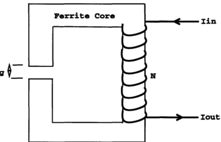
The inductor is implemented using 8 turns of circuit board 3oz copper wound over a rectangular ferrite core. The effective implementation is as shown in Fig. 2-6. The core used has an effective area A equal to 19.5 x 10⁻⁵ sq. meters; N = number of turns=8; the gap g is given by:
N2
A-g
9o
Ferrite Core
---
Iin
I
IN
I O Iout
Figure 2-6: Effective inductor implemented
2.2 Issues in Paralleling Converters
2.2.1 Interleaving
The converter designed in this thesis has four 28 W down-converter stages in parallel each operating at 250kHz. Among other benefits, paralleling in this manner ensures that current flows through four times the amount of silicon and copper. For a con-verter with excess conduction losses even when the largest MOSFETs are being used, this technique helps to alleviate the problem.
Some of the switching losses seen in a converter are comprised of energy that is stored in in parasitic inductances and capacitances and lost during switch transitions. These switching losses can be reduced by use of the parallel approach. If two switches, each with resistance R, are used in parallel and out of phase, some effective switching losses will be seen. However, if a single switch with a resistance of value R/2 were used instead at the same effective switching frequency, the switching losses are doubled because the effective capacitance of the switch would be twice that of the switch with
resistance R.[4]
The four converters are interleaved to sum four evenly phased waveforms to form the bus current. This gives us a bus current that switches with a frequency 4 times the single converter frequency of 250kHz. Generally for N interleaved converters the
I I I
r
I
I
frequency will be N times each converter frequency giving us a factor of 1/N reduction in the size of filter elements required. Furthermore, since the line power is evenly distributed among the N converters, a correspondingly small disturbance will need to be filtered, allowing for another 1/N reduction in the size of filter element. Hence a total reduction of 1/N2 is attained in the size of filter elements. This improvement
can either be exploited by reducing the size of filter elements or by operating the converter at a lower switching frequency to reduce switching losses. The final choice is an optimization that aims to capture the best of both effects.
2.2.2
Layout
The gains we get from interleaving converters come with a few penalties. By in-terleaving, we have split up our current path into four identical cells, so that each cell now carries 1/4 as much current as it would ordinarily, for the same voltage
transfromation. The major disadvantages to this setup are:
* Interleaving requires the current to be equally shared among the converters. In continuous mode operation, ensuring this balance would require a current monitoring system. In this thesis, the down converters have been designed to operate in the discontinuous mode ensuring that any imbalance in the current sharing is only a factor of discrepancies in cell inductance or in the switch duty-ratio. The duty-ratios can be easily maintained within 1% of each other. With careful layout, the cell inductance is easily kept within 5% of each other. Assuming total independence of these two factors, the worst case variation in cell currents is within 6%, an acceptably small value.
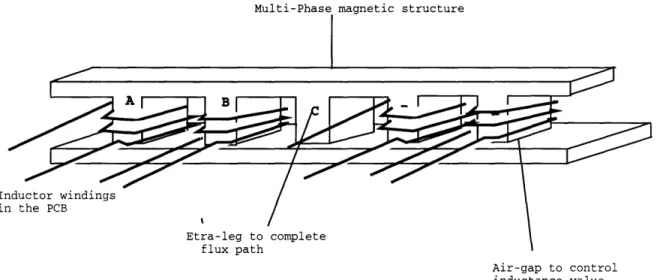
* Interleaving also requires that for each converter a greater value of switching inductance be used. The amount of inductance required for each converter is directly proportional to the number of converters connected in parallel. This requirement is a direct comprise on our desire for miniaturization outlined in Chapter 1. This problem was solved by developing special multi-phase magnetic structures in which flux through one cell of inductor windings is made to cancel
out flux from adjacent inductor windings. A pair of adjacent core legs is used to make adjacent inductor windings wound in opposite directions and operated out of phase. However since the current through each of these windings is triangular, the flux waveforms do not exactly cancel each other. An extra core leg is necessary to return the excess flux. Furthermore, since a controlled value of inductance is required, an air-gap is used in the core. The extra core leg is therefore necessary to complete the flux path. Figure 2-7 shows the inductance
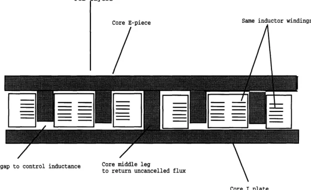
core piece with the windings. The cross-section of the windings as they appear on the board is shown in Fig. 2-8.
I] i]
Air-gap to control inductance value
Figure 2-7: Multi-phase structure used to build the parallel converter inductance
. . .
*-PCR avers
Core E-piece Same inductor windings
A\
Air-gap to control inductance Core middle leg
to return uncancelled flux
Core I plate
Figure 2-8: Cross-section of the inductor windings , y __
Chapter 3
The Isolation Stage and Output
Filter
As stated earlier, an isolation transformer forms the second stage of the two-stage converter designed. This chapter summarizes the basic operating principles of a push-pull converter. It also presents the details of the particular push-pull converter designed and constructed in this thesis.
3.1 Push-pull Converters
A push-pull converter operating at 100% duty-cycle is used to provide isolation and to step down the intermediate bus voltage to the desired logic level of 5V. The voltage regulation in this circuit is provided entirely by the down-converter stage discussed in Chapter 2. Since the isolation stage is free from regulation requirements, it can be operated open loop, which requires a relatively simple control mechanism. The push-pull converter has either one or the other switch conducting at all times.
3.1.1
Operation
The basic configuration of a push-pull converter is illustrated in Fig. 3-1. When the switch Q1 is turned on, a voltage v = vu, is applied across the primary coil of this branch. This voltage builds up a current i in the magnetizing inductance of the
N:n id d2
Iin
-- I
ut
Figure 3-1: Basic push-pull stage
primary coil at a rate approximately equal to L7ai .i . This current continues to
grow until Q1 is turned off at half the period of operation and Q2 is turned on. When this happens some of the current continues to flow in the parasitic capacitance of the switch Q1, while it builds up in the magnetizing inductance of the Q2 branch.
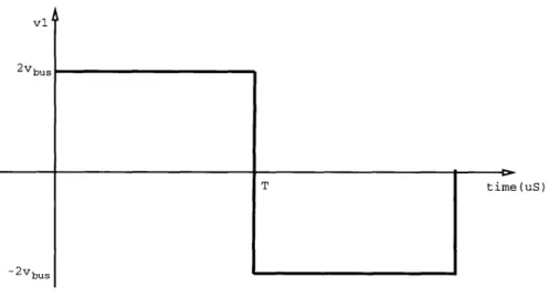
When the switch Q1 is turned off, and Q2 turned on the current in Q1 continues to flow in the same direction for half the period, while collapsing towards zero. Mean-while, the drain of Q2 will swing in voltage from 2vbU above the bus level to 0. The voltage at the drain of Q1 will rise up ideally towards infinity. However, since the drain of Q2 will be held at zero, the voltage across the magnetizing inductance of the Q1 branch can only go as far as 2vuJ,. This reverse voltage will be integrated to give the current i which reverses direction by the end of the cycle. Figures 3-2 and 3-3
show the resulting curves for primary voltage val and primary current il respectively.
Operating the push-pull stage at 100% duty-cycle ensures that the voltage stress on all the components is constant over all conditions of operating voltage and input
T time (uS)
Figure 3-2: Resulting curve of transformer primary voltage
Vbus
.5T T
Figure 3-3: Resulting transformer primary current
A vl 2Vbus -2vbus Ip] -Ipk' I . Eb I
power level. For the required output voltage, the voltage stress on the switches and rectifiers is minimized. 100% duty-cycle also ensures that the core material of the transformer is better used because of the double-ended nature of the push-pull topology.
3.2 Design of the Isolation Stage
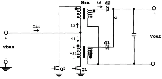
The basic constraints to be met were:
1. A 6:1 step-down transformer ratio. The intermediate bus voltage is set at 30V. We wish to obtain a 5V output digital logic drive signal.
2. We desire a high efficiency performance. Thus, the switching losses in this circuit must be set to a minimum.
3. The circuit must occupy as little space as possible.
3.2.1
Topology
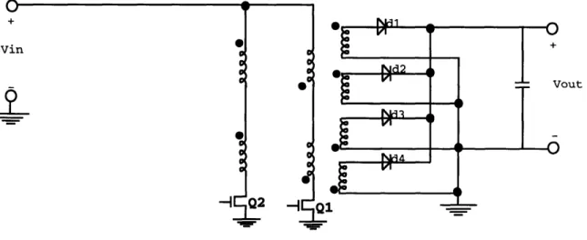
The basic design therefore is one which uses six turns in the primary and one turn in the secondary. The choice of these numbers (as opposed to something like 12 primary turns and 2 secondary turns) is justified in the section below. In the implementation each transformer is a series connection of two transformer blocks each of which has
a 3:1 ratio. Distributing the transformer coils in this manner allows us to use fewer layers of the PC Board into which the transformer is integrated. By using fewer PCB layers, the proximity effects are reduced. The 30 voltage intermediate bus voltage divides equally between the two transformer blocks so that the effective turns ratio is still 6:1. The topology is illustrated in Fig. 3-4.
Ordinary implementation of this transformer would require more in terms of core volume and consequently core losses than when simple 6:1 stages are used. We exploit the fact that flux in phased magnetics in multi-phase magnetic structures can be made to partially cancel each other. Special magnetic structures are designed whose core legs are built in such a way that phased flux in one leg partially cancels the flux in
Vin 0 0 0 0 0 S C a C 0 a a a C 1_1_ I/Id2 4 7o
_E~I
Figure 3-4: Topology of Push-pull stage designed
another leg. In ac-ac transformers, the waveforms are sinuisoidal and the flux in each of the legs exactly cancels the flux in another. By wounding adjacent coils in opposite direction to each other, the triangular waveforms of this transformer can be made to cancel each other. However, an extra leg is provided to return remnant flux in cases where flux may not be completely balanced. This leg serves as a protection against faulty winding, or unbalanced flux linkage.
By using this magnetic core structure, the required volume of the transformer is greatly reduced. The structure provides adequate surface area necessary to keep the transformer cool. Furthermore, due to the fact that individual return legs are no longer needed for each transformer core leg, the total core loss is greatly reduced. Using the spread-out transformer blocks requires very few windings per block, a quality we exploit by using spiral windings formed in a four-layer PCB.
The four windings required for the transformer blocks are arranged on the outer legs with adjacent windings done in such a manner that their flux almost cancels out. The remnant flux is returned through the middle leg. The interaction of the flux
+ Vout l . r I i I ____j I L v VI 4 I I r- _ __LA IU %-
._
through the legs gives a magnetizing current through the windings that is slightly different from the triangular waveform expected in conventional dc-dc transformers. Note that since an infinite magnetizing inductance is desired, the core legs are not gapped. The transformer core design is shown in Fig. 3-5 below.
E-core piece
Multi-Phase magnetic structure
I-core piece
Etra-leg to complete flux path
Figure 3-5: The multi-phase magnetic transformer core
3.2.2
Design Considerations and Discussion
The most basic consideration to be made when designing a transformer is the turns ratio. While this is easy to meet, considerations of the power handling capacity, and core saturation must be made. The transformer designed is required to meet the following specifications:
* Input voltage, nominal 30V dc
Secondary Coil P1B layers Core E-piece
I
Same Primary coil
A
~~/ ~Core middle leg
Primary coil to return uncancelled flux
Core I plate
Figure 3-6: Cross-section of the transformer stage * Operating frequency 1.0 MHz
* Output Voltage 5V
* Output Current 50A
The core selected ferrite P-typel from Magnetics Inc.2 with a saturation flux density of .35T at 100°C. The transformer is designed to allow for a maximum swing in flux density equal to ABma,, = .200T. This value is arbitrarily selected, but it ensures that the transformer stays clear out of saturation. Considering the secondary coil, the optimum turns per volt may be calculated as follows:[l]
N/V =
ABra X Ae
* N/V = optimum turns per volt
1See Appendix for P-material characteristics
2
*
to = maximum "on" time, uS
* Ae = area of core, mm2
In this thesis, Ae = 19.5mm2, to, = 0.5uS,, which gives a turns to volt ratio of 0.128. The output voltage on each of the secondary coils is the amount enough to support a total voltage of 5.5V,(nominal output of 5V plus any diode and other miscellaneous losses). This gives an optimum number of secondary turns of 0.69. Since the number of turns must be an integer value, we round this value to the nearest whole number of 1. This rounds the new turns to volt ratio to 1/5.5 = 0.182. The primary number of turns for a primary voltage of 30V becomes 0.182 x 30 = 5.46 which is again rounded to the integer value of 6 turns.
For switching purposes IRFD1203 n-channel MOSFETs are used. IRFD120 MOS-FETs have low on-resistance, 0.3, 1.3A average current rating and 100V drain-source voltage rating.
3.2.3
Losses and Energy Recovery
The switch transitions in the isolation stage can cause significant losses. There are two methods through which this loss can be incurred:
* When the switch is turned off, the voltage at the drain rises even though some of the current continues to flow down the channel. The product IV across the channel can be a significant part of the circuit's dissipation.
* When a switch is turned on, parasitic capacitance at the drain node is discharged through the channel. At turn-on, the current will again begin to flow through the channel before the drain-source voltage has completely dropped to zero. In order to alleviate the first loss mechanism, turn-off, a clamp circuit is required to provide an alternative low resistance path for the current when the switch is turned off. The excess charge flowing at turn-off is dumped onto an energy recovery capacitor
3
Ge via a diode, as shown in Fig. 3-7. This capacitor is made large enough to hold all
the charge that will build up as the current collapses in the magnetizing inductance. As discussed earlier, the voltage of this capacitance which follows the drain voltage will rise to double vo when the switch is turned off, and a varying resistance path is provided to discharge this capacitance as shown in Figure 3-7. The two resistors
R1, R2 are chosen such that when the voltage drop across them is greater than 2v,,
the drop across R1 turns on the zener Ze and forward biases the transistor Tq creating a low resistance path back to the source. An ordinary 2N3904 BJT was used for Tq,
Ze is a 5.1V zener diode, and R1 and R2 are 4.7K and 56K respectively. The reason
the resitors are chosen this way, is due to the fact that for the push-pull stage to perform as required, the voltage at the drain must be allowed to swing to double the bus voltage.
Iin
dl
1
Figure 3-7: One branch of the Push-pull showing the energy recovery circuit.
vb
3.3 The Output Stage
At 20 A, the output current rating requires extremely low resistance and diode drop to keep power dissipation down. The primary objective is to keep the dissipation due to the output diodes substantially low. When the push-pull stage is operated at 100%
duty cycle and with total current balance, the output current is shared equally among the four interleaved output diode paths. With each carrying an average current of 5 A, a drop of Vd across each diode would mean 4x5Vd W dissipation. International Rectifiers, Inc. manufactures 19TQ015 "Or-ing" diodes with a forward voltage rating of 0.24V at 8 A average current. Although these diodes come in TO-220 packaging, a related D-pack surface mount family is available from Motorola.4 In this circuit 19TQ015 diodes were used for the output rectification.
The current through each output diode ripples ideally between 0 and 10A. With interleaving, the aggregate output current will be the sum of the four diode currents. Thus the output current should ideally ripple between 0 and 20 A. However, because of the reflected leakage inductance from the primary of the transformer, the current rippling is greatly reduced. Further, a large high frequency output capacitance is used to lower the output voltage ripple.
Chapter 4
The Control: Putting it all
Together
This chapter is a discussion of the control mechanism used to operate the power converter designed. The converter design values outlined in Chapters 2 and 3 are chosen so as to satisfy the specifications when the converter is operated open-loop.
4.1 Types of Drivers Required
Like in every multi-phase power converter, the converter designed in this thesis called for a mechanism to drive both high-side switches and low-side switches. High-side switches in this case refer to those switches which are driven relative to a constant reference voltage value that is above ground. The reference voltage is the bus voltage which may be the input voltage for P-channel MOSFETs or a circuit-created reference that stays approximately constant for both P-channel and N-channel MOSFETs. Low-side switches refer to those switches whose gate is driven relative to ground.
4.1.1
High-Side Driver
In the power converter described above, the two stages are connected in series. Since each of the stages has switches associated with it, the switches of the stage that comes ahead of the other along the current path will inherently have to be driven relative
to some no-zero voltage. The connection of a single current path is as shown in Fig. 4-1. + Vin -I~~~~ a a a
r-~~~~~
rni / _.~-
Q2i
o a aE7
tO .LJI
HL Q1 I1 b OrRo Vref + , T__~ r iFigure 4-1: The complete path of current through the circuit.
In this figure, the switch Q1 is high-side because its gate is driven relative to a voltage v,ef shown in the figure. A high-side driver is therefore required to operate this switch. The particular signal to drive the gate of this switch is produced using either an oscillator or a simple clock. In order to actually use the signal, the signal must be produced from a floating ground source, such as a battery, or a mechanism be used to couple the signal to the new reference v,rf. There are several suggested mechanisms for achieving this floating ground, but each comes with its costs. The deciding factor as to whether or not to use a given type of high-side driver is based on estimated power requirements of the driver, its cost of implementation and how well it fits with the general moral of the design. In this case, a low loss, small-sized driver is required. Investigations into driving high-side switches is an active research area. In this thesis, several voltage coupling methods were investigated. The final selection was one in which a zener diode is used to provide the turn-on voltage. The topology used is as shown in Fig. 4-2.
When the switch Qd is turned on (when the drive signal is high), the zener, Ze, is forward biased. Thus the voltage Vgo across the gate-source nodes of the MOSFET
.1 r. -3 l P I
_
_ I/"= I -I I-,~ W4" 1 %. IV D1 Vs
T
_JT-L_
Drive SignalFigure 4-2: Suggested driver unit for the high-side switches
V1T
V
I
V,
I
- O
Nd2 4 0 .EE4 out Wl.1 VQ1 used as high-side switch will be approximately zero; the switch will be off. When the drive signal goes low, the switch Qd is turned off, and a current path will be established through R1 and the zener Ze. The zener will be reverse biased and will turn on with voltage of 10.5V, the diode's rating. This will mean a 10.5 drop across the gate-source nodes of the high-side switch Q1, which is sufficient to turn it on.
In doing this, we are creating a second path of current from the high voltage source. This path is dissipatory and adds to the reduction in the efficiency of the overall operating unit. However if big resistance values are chosen for the two resistors R1 and R2 shown, the current that flows through them can be greatly reduced and consequently their power dissipation can be kept at a minimum.
Essentially, the power lost by use of this setup is approximately:
(Vus - V)2 (V8)2
Qd
= +R1 R2
Pq
V.
(V
+
10.5))2
((V
10.5)))
-
(v
+
PPddf f R1 + 10.5( R1
As stated earlier, large values of R1 and R2 are used to ensure low I2R losses
across resistors. Tests performed on this driver showed that its performance is largely dependent on the gate-source capacitance of the switched MOSFET. The large value of resistance used means that the turn-on, turn-off time constant can no longer be neglected. An optimum level is chosen to operate each particular MOSFET.
4.1.2
Low-Side Driver
The switches in the down converter are driven relative to ground i.e. they are low-side switches. Since drive signals are themselves produced relative to ground, no coupling is necessary to operate the low-side switches.
4.2 Drive Signals and Implementation
This section describes the circuit used to provide the various signals required to drive the switches used in this circuit. The converter is operated open loop using pulse-width modulated signals produced as described below.
4.2.1
Drive Signals
The drive signal required to implement the switching function q(t) are square wave signals produced and which are duty-ratio controlled. There are four basic operations involved in producing the duty-ratio controlled four-phased signals to drive the low-side drivers.
* Production of the basic timing signal
This sets the frequency of the clock used to produce the drive signal. It is produced by a two inverter oscillator clock configured as shown in Fig. 4-3. The design of the control requires that the clock frequency be 1MHz if the drive signals are to be 250kHz.
Inverter
r~~~~rr04~CI.; L.I
Figure 4-3: Clock implementation: make R1 > R2.
To get a clock frequency of 1MHz, R1 is chosen to be 22K, R2 =4.99K and C = 33pF. This means that charging or discharging of the capacitor will have
a time constant given by R2C. Motorola's1 MC14069UB Hex Inverter is used
libid: Motorola Corp
- . W n&'r ( I
to provide the required gates. The frequency obtained from this connection is found to be about 980kHz. If R2 is made adjustable, the frequency can be adjusted as desired.
* Phasing out the different signals
Having set the operating frequency as discussed above, the next step is to pro-duce the phased signals to be used to drive the switches. The clock signal is fed into two LT14027 J-K flip-flops2 to provide the necessary switching waveforms.
Each pair of the resulting waveforms is selected via an "AND" gate to perform the phasing. An MC4081 is used to provide the necessary "AND" functions.
* Duty-ratio control and buffering
In order to drive the switches at the required duty-ratio, the signals produced above must be pulse-width modulated. First, the square wave produced is converted into a sawtooth signal by the use of the circuit shown in Fig. 4-4. 2N7000 MOSFETS are driven with the signals produced above. When the MOSFET is off, a resistor is used to charge a capacitor exponentially with an RC time constant towards a set bias voltage. This happens until the drive signal is high, (MOSFET on), when the capacitor is discharged through the short circuit created by the MOSFET.
The only design requirement is that the time constant for charging the capacitor should be much greater than 4us, the period of the square wave. The resistance is chosen to be 22K, while the capacitor is selected to be 100pF.
The next step involves pulse-width modulating this signal. This is done by comparing the sawtooth waveform to a set reference voltage value. Motorola's LS311 voltage comparator is used to for this purpose. The output signal will only be high when the sawtooth is higher than the reference value. By changing the reference value, the duty-ratio of comparator output can be controlled. Micrel's3 MIC427CM power MOSFET drivers are used as the buffering stage
2LT14027 by Texas Instruments Inc., P.O Box 809066, Dallas, Texas 75380 3
Vbias R I I I I o- Q Input Waveform I
_
PA
A-Output Wave
C
T
Figure 4-4: Implementation of sawtooth waveform used in PWM.
to drive the switches. These drivers have a peak output current of 1.5A, and an output resistance of 6 ohms.
4.2.2
Implementation
Figure 4-5 gives a detailed diagram for the control used. The values of resistance and capacitance are chosen to set the particular duty-ratio, operating frequency, and other circuit parameters as discussed above.
I
IMI I I
-1
E
a z
F'igure 4-5: The Control Circuit: a detailed diagram.
I
S!
II
7
Chapter 5
Testing and Experimental Results
This chapter describes the testing and performance of the two stage converter con-structed. The tests were done in two steps. First, the down converter stage was tested for different values of input voltage. Next, tests were performed on the push-pull stage to establish its behavior. Each of these tests were performed with respective loading mentioned below. It is worth noting that during the testing, the MOSFETs tended to heat up more than expected even for currents much lower than the manufacturer's rating. As a result, the tests could not be performed for high input power as this
destroys the MOSFETs. The reason why the MOSFETs did not perform as expected may be due:
* Electrostatic exposure of the MOSFETs may have deteriorated the compro-mised their perfomance. In building the prototype, there was a lot of human handling of the MOSFETs, which may have led to their electrostatic weak-ening causing serious leakage. This effect is further asserted by the fact that even when the gate-source voltage of the MOSFETs is held at zero, there was significant leakage.
* Initial tests on the MOSFETs showed that the value of voltage required to turn them on was a fairly large range, (3V-18V). The performance of the MOSFETs however, depend on the this drive voltage in terms of leakage. One notices that the higher the drive voltage, the higher the drain source leakage. This
is due to the fact that the gate-source capacitor voltage holds on for a time
which is dependent on the RC time constant it 'sees'. Thus the high the initial
gate-source voltage, longer it takes for the voltage to decay to the turn-off value.
5.1 Testing the The Down Converter
Two tests were performed on the down converter. The first test was to establish the relationship between the input and output voltages of the converter, and assess the
ripple of the output for a constant input voltage. The second test was to study the
effects of interleaving, and current sharing. This test is also used to demonstrate that the converter is a current source rather than a voltage source.
5.1.1 Experimental Results
A single down converter was operated to study its open loop input-output charac-teristics. Data was obtained for the values of input voltage, output voltage, source current and output ripple. The converter is used to drive a 75F resistance load, with a filter capacitor of 3uF. The input voltage is filtered through a 47uF capacitor. The results presented here are an average of readings taken. The duty-ratio used was 0.23, with a switching frequency of 250kHz. Fig. 5-1 shows a snap of one of the measurements taken. The plots shown on the screen are input voltage (30V), output voltage and the drive signal.
Results of several such measurements are presented in Table 5.1.
Figure 5-2 shows the relationship between Vout and Vin. The dashed curve shows the ideal value of Vout when the duty-ratio is as calculated (23%). The gradient of the curve of the measured results gives the actual duty-ratio of 22%. Thus within a 1% error, the input-output voltage relationship of the down-converter is satisfied.
The relationship between the output ripple and the input voltage is also plotted. The ripple is directly proportional to the input voltage with the constant of propor-tionality being the duty-ratio, the operating frequency, the circuit inductance L, and the capacitance C, used for filtering. With L= 50uH, C=3uF, F=250kHz, D=0.23,
T l i x , "
Figure 5-1: Snapshot
signal.
showing the input voltage, output voltage, and switch drive
Table 5.1: Table of Results for a Single Down Converter. Vin (r) Vbus(V) Vout=Vin-Vbus DVin(V) Vripple(mVpp)
15 11.4 3.6 3.45 62 20 15.3 4.7 4.60 68 25 19.0 6.0 5.75 76 30 23.0 7.0 6.90 84 35 27.0 8.0 8.05 92 40 31.2 8.8 9.2 100 50 40.8 9.2 11.0 108
I
Plots of Measured Vout, and DVin (dashed) versus Vin
Input Voltage (Volts)
Figure 5-2: Input-Output voltage relationship for a single down converter.
1 0a ., 0) 0 Q.
0
the constant of proportionality is approximated as:
4 (DT)2
K = ()=
1.13mV/V
5 4LC
The experimental value for this constant is the slope of the curve and is obtained to be 1.387mV/V. Given the possibilities of error in the inductance calculation, and the ignored resistive effects in the circuit, this value is acceptable within these
exper-imental limits.
Plot of Output Ripple versus Input Voltage
15 20 25 30 35 40 45
Input Voltage (V)
Figure 5-3: Relationship between output ripple and input converter.
voltage for a single down
1
>
E v a) 03Q. Q.0
50Figure 5-4: Picture showing a set of measurements taken for operated out of phase.
two down converters
The next set of tests were performed with two down converters operated 90° out of phase. The snapshot of the type of measurements taken is shown in the Fig.5-4 which shows a set of input and output voltage and the switch drive signals showing the switches are operated out of phase.
With the same output load as in the single converter case above, the results obtained are presented in Table 5.2.
Since the same load is used in both cases above, comparing the two tables directly should give answers to questions we hoped to address. If the two converters are indeed
Table 5.2: Table of Results for Two Down Converters Operated out of Phase. Vin (V) Vbus(V) Vout=Vin-Vbus DVin(V) Vripple(mVpp)
15 8.2 6.8 6.90 70 20 10.9 9.1 9.20 82 25 13.6 11.4 11.50 106 30 16.6 13.4 13.8 114 35 19.6 15.4 16.1 130 40 22.4 17.6 18.4 144 _ __ ___ _ ___
edentical and in parallel, two times as much current should be flowing through the load as it did when a single converter was used. This would mean that for the same input voltage,and with the same load, the output voltage should be double, I x R. Indeed, this is seen to be the case.
Without interleaving, the output ripple would now be expected to double. This is because, double as much current as in the case of a single converter is drawn, hence the total change in charge transferred has doubled. However, interleaving greatly reduces this effect to a value comparable to the case when a single converter is used. Indeed, if the desire was to obtain a given output voltage, the two parallel down converter setup would be favorable because it would be operated at half the voltage of the single converter, which from the Tables 5.1 and 5.2 means approximately half the output ripple of the single converter.
5.2 The Isolation Stage
For the isolation stage, the tests done were primarily to determine the flux linkage by establishing the relationship between the input and the output voltages. Since the transformer stage is not used to perform voltage regulation, the main interests of tests performed centered on the perfomance turns-ratio transformation (flux linkage) and the energy recovery bipass.
5.2.1 Experimental Results
The push-pull stage is operated with a 20V input voltage and the characteristics of output voltage and energy recovery circuit studied. As mentioned in Chapter 3, the push-pull stage is operated at a 100% duty ratio, and it is zero switched. The output voltage is obtained to be 3.3V. This gives a turns ratio of 20/3.3 which is about 6:1 as expected. This satisfies the requirements on magnetic coupling between input and
output transformer coils.
With this input voltage, the output ripple is observed to be 120mV. This is satis-factory. The design ripple (acceptable ripple) was set at 50mV with four interleaved