HAL Id: hal-02549953
https://hal-cnrs.archives-ouvertes.fr/hal-02549953
Submitted on 5 Nov 2020HAL is a multi-disciplinary open access
archive for the deposit and dissemination of sci-entific research documents, whether they are pub-lished or not. The documents may come from teaching and research institutions in France or abroad, or from public or private research centers.
L’archive ouverte pluridisciplinaire HAL, est destinée au dépôt et à la diffusion de documents scientifiques de niveau recherche, publiés ou non, émanant des établissements d’enseignement et de recherche français ou étrangers, des laboratoires publics ou privés.
Investigation of KBiFe2O5 as a Photovoltaic Absorber
Thomas Fix, G. Schmerber, J.-L. Rehspringer, C. Leuvrey, S. Roques, M.
Lenertz, D. Muller, H. Wang, Abdelilah Slaoui
To cite this version:
Thomas Fix, G. Schmerber, J.-L. Rehspringer, C. Leuvrey, S. Roques, et al.. Investigation of KB-iFe2O5 as a Photovoltaic Absorber. ACS Applied Energy Materials, ACS, 2019, 2 (11), pp.8039-8044. �10.1021/acsaem.9b01509�. �hal-02549953�
1
Investigation of KBiFe
2O
5as a Photovoltaic Absorber
T. Fix
1*, G. Schmerber
2, H. Wang
3, J.-L. Rehspringer
2, C. Leuvrey
2, S. Roques
1, M. Lenertz
2, D.
Muller
1, H. Wang
3,4, A. Slaoui
11
ICube laboratory (Université de Strasbourg and CNRS), 23 rue du Loess, BP 20 CR, F-67037
Strasbourg Cedex 2, France
2
Institut de Physique et Chimie des Matériaux de Strasbourg (IPCMS), UMR 7504 CNRS and
Université de Strasbourg, 23 rue du Loess, BP 43, F-67034 Strasbourg Cedex 2, France
3
School of Materials Engineering, Purdue University, West Lafayette, IN 47907, USA
4
School of Electrical and Computer Engineering, Purdue University, West Lafayette, IN
47907, USA
* Corresponding author. Tel.: +33 388106334, Fax +33 388106548. E-mail address:
tfix@unistra.fr
Abstract
KBiFe2O5 (KBFO) was grown by pulsed laser deposition (PLD) on SrTiO3 (001) (STO), 1 at% Nb-SrTiO3
(001) (Nb-STO) and MgAl2O4 (001) (MAO). In the case of MAO substrate, epitaxial growth is obtained.
As its bandgap is relatively low (1.6 eV in the bulk), KBFO is a promising candidate for oxide photovoltaics. In this work we examine the growth of KBFO by PLD by looking at its structure and composition and we investigate the optical properties of the films obtained. A photovoltaic architecture based on KBFO films is proposed and a solar cell behaviour based on KBFO absorber is obtained.
2
Introduction
Thin film solar cells in industry are mainly based on CdTe, amorphous Si and CuInGa(Se,S)2 (CIGS). In
recent times research on hybrid perovskites expanded exponentially, with solar cell power conversion efficiencies above 21%. This proves that research on novel materials for solar cells can be quite successful and should be maintained. Standard solar cells are based on a pn-junction, however ferroelectric solar cells have emerged with a record conversion efficiency in Bi2FeCrO6 of 8.1% (1,2,3).
In this type of solar cell, there is no need for a pn-junction and the charge separation can originate from the polarization due to the ferroelectricity (4). The most studied ferroelectric material for its photoelectric properties is BiFeO3 (5). It was discovered that open circuit voltages of more than a
dozen volts could be obtained with this material, and that it is linked to the ferroelectric domain walls (6). Still, ferroelectric solar cell efficiencies with BiFeO3 are generally much below 1% and the
BiFeO3 bandgap of around 2.6 eV is not ideal for the solar spectrum (7). In fact, oxides with a
bandgap suitable for the solar spectrum around 1.3 eV are scarce. Examples of such oxides are 1.1 eV for LaVO3 (8), 1.2 eV for BiMnO3 (9), 1.2 eV for CuO (10) and 1.5 eV for Co3O4 (11), but these
examples provided low solar cell conversion efficiencies pointing out that other parameters than the bandgap must be taken into account to provide efficient solar cells, such as carrier density and carrier diffusion length. Therefore alternative materials are welcome.
In this perspective, KBiFe2O5 (KBFO) was reported in 2013 as a new ferroelectric compound with a
bandgap of 1.6 eV and a high Curie temperature of 780 K (12). Measurements on single crystal KBFO contacted with Ag electrodes led to a high open circuit voltage (Voc) of 9.1 V and a short-circuit
current density (Jsc) of around 15 µA/cm² (12). Other studies on bulk KBFO exhibited a photoresponse
with Voc=2.04 V, Jsc=20.7 µA/cm² (13), and Voc=-0.5 V and a short circuit current of 20 nA (14). It was
argued that the short-circuit current density was limited due to the fact that measurements were made on single crystal KBFO. Thus, the synthesis of KBFO layers using a sol-gel process and spin-coating has been reported (15,16). KBFO has a brownmillerite type-structure A2B2O5 with lattice
parameters a=0.7984 nm, b=1.1819 nm, c=0.5739 nm with an orthorhombic space group P21cn (12).
In addition, magnetoelectric and photovoltaic (PV) effects in KBFO were studied theoretically in (17). In the present work, we investigate the growth of KBFO in the form of thin films using the pulsed laser deposition (PLD) method. PLD is known to result in high quality materials, in particular in the case of an expitaxial process. The structural and optical properties of the deposited KBFO films are reported.
3 The KBFO target used for the PLD process was prepared as follows. First potassium nitrate (4.936 g), bismuth (III) nitrate pentahydrate (26.973 g), and iron (III) nitrate nonahydrate (27.234 g) are poured in deionized water (~100 ml). Films deposited from a stoichiometric composition were shown to be largely K and Bi deficient. Therefore targets were made with an excess of K and Bi in the following proportions: K 1.45:Bi 1.65:Fe 2. Citric acid (14 g) is dissolved in the solution together with ethylene glycol (30 ml, the Pecchini method is used). The excess of water is evaporated and a viscous liquid without precipitate appears. This compound is pre-calcinated in a furnace at 350 °C for two hours, mechanically ground in a mortar, and further calcinated at 700 °C for 1 h in air. The obtained powder is ground again, pressed into a pellet and sintered at 700°C for 1 h in air. The target is thoroughly polished, as Rutherford Backscattering (RBS) has indicated that the surface of the target after sintering is mainly composed of K. It was checked that the composition of the polished target matches the stoichiometry of the precursors.
The PLD process was performed using a KrF laser with 10 Hz repetition rate and a laser fluence of around 2 J/cm2 on the target. The substrates used for deposition were SrTiO3 (001) (STO) (insulating,
thickness 0.5 mm), 1 at% Nb-SrTiO3 (001) (Nb-STO) (resistivity 0.003 Ω·cm, thickness 0.5 mm) and
MgAl2O4 (001) (MAO) (insulating, thickness 0.5 mm). The deposition was carried out at 700 °C under
an oxygen pressure of 10−2 mbar. KBFO film thicknesses were in the 50-100 nm range. The as-grown film was cooled down under the same atmosphere at a rate of 10°C/min until 300°C, below this temperature it was naturally cooled down until room temperature. Around 30 samples were deposited for the study.
The crystalline structure of the KBFO films was analyzed by X-ray diffraction using a Rigaku SmartLab diffractometer equipped with a monochromatic source delivering a Cu Kα1 incident beam (45 kV, 200
mA, 0.154056 nm). X-ray θ−2θ and reflectivity were performed in order to look for the film structure, check the presence of spurious phases, and determine the film thickness. Scanning electron microscopy (SEM) was performed with a Gemini 500-ZEISS apparatus. Rutherford backscattering was used to determine atomic composition and thickness of the layers, using 1.5 MeV He+ particles provided by the Van De Graaff Accelerator (HVEE KN4000) facility of ICube. Transmission electron microscopy (TEM) was performed with a FEI TALOS F200X TEM/STEM with ChemiSTEM technology (X-FEG and SuperX EDS with four silicon drift detectors) operated at 200 kV. It was used for microstructure characterization and energy-dispersive X-ray spectroscopy (EDS) chemical mapping. The optical measurements of the KBFO films were investigated using a Perkin-Elmer Lambda 950 spectrophotometer using a 150 mm integrating sphere. Their ferroelectric properties were investigated by the Piezoresponse Force Microscopy (PFM) technique using a Bruker Icon QNM
4 microscope. For PV measurements, I-V characteristics were carried out at room temperature using an Oriel Solar Simulator in AM1.5G conditions and a Keithley 2461 SourceMeter.
Results
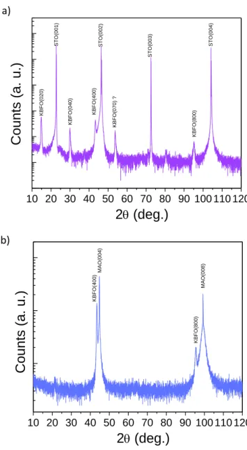
Firstly KBFO was deposited by PLD on SrTiO3 (001) (STO). The XRD θ–2θ pattern was recorded as
shown in Fig. 1a). STO is cubic with a lattice parameter of 0.3905 nm. Because there is no direct match between the STO substrate and KBFO, two different orientations are observed, (020) and (400). In the search for more suitable substrates, MgAl2O4 (001) (MAO) was used. It is also cubic but
with a lattice parameter of 0.8083 nm. Fig. 1b) shows the corresponding XRD θ–2θ pattern. The two film peaks observed can be attributed to KBFO (400) and (800) and no other parasitic peaks are observed within the limits of the technique available. The possible epitaxial relationship is KBFO [010](100) // MAO [110](001), confirmed by TEM observation (see Supporting Information (SI) Fig. S1). In this situation the KBFO b and c lattice parameters are compressed in plane by 3.4% and 0.5% respectively compared to the bulk, which generates an extension of the a lattice parameter. Hence according to XRD the KBFO a lattice parameter is 0.8321 nm which is about 4.2% larger than the bulk. It should be noted that the KBFO (200) and (600) reflections are absent, which could originate from strain or defects, and indicates that the film deviates from the P21cn space group of the bulk (12).
SEM analysis performed on KBFO on STO (001) revealed a growth with elongated rectangular shapes while smoother films could be obtained on MAO (001) (see SI Fig. S2). Analysis of the stoichiometry by EDS showed that the sample is composed of K1Bi1Fe3.3Oy (SI Fig. S3). However, the measurement
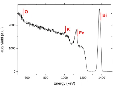
of stoichiometry in this case is not very accurate. This is due to the overlap with Sr and Ti signal from the substrate and also due to the small thickness of the sample (60 nm). Inaccuracy of the EDS analysis has been previously observed in similar materials based on Bi (3,18). In order to better account for the stoichiometry we performed RBS analysis on a KBFO//STO (001) film as shown in Fig. 2. The analysis for the spectrum using the SIMNRA tool indicated a stoichiometry of KxBi1Fe2.2Oy while
the stoichiometry of K and O could not be determined in this analysis. The uncertainty of the values obtained for stoichiometry by RBS is 5 % for each element. Therefore we are confident that the stoichiometry obtained in Fe is not far from the desired K1Bi1Fe2O5 material.
In order to better understand the growth of KBFO, TEM was performed. Figure 3 shows TEM observations of a KBFO thin film on MAO (001) along the MAO [100] zone axis. High epitaxial quality thin film is observed by TEM (Figure 3c, SI Figure S4, S5). The electron diffraction pattern (DP) (Figure 3b) and high-resolution TEM (HR-TEM) image show the great lattice matching between film and
5 substrate and confirm the epitaxial relationship proposed above. However, further work will be to accurately determine atomic positions for comparison with the proposed bulk structure in (12).The EDS mapping shows Bi segregation in the film (Figure 3d, SI Figure S6), while K and Fe are evenly distributed in the film.
We now focus on the optical properties of the films. Figure 4 shows the optical absorption properties of the MAO (001) substrate and a 60 nm thick KBFO film on MAO (001). The absorbance was not corrected for reflection. It shows that despite the low thickness the film is absorbing well in the 200-600 nm region. The Tauc plot is shown in the inset of Figure 4, showing a direct bandgap of around 2.3±0.1 eV. This value is larger than the value obtained for bulk KBFO (1.6 eV) (12) but slightly lower than KBFO thin films fabricated by chemical solution deposition (2.5 eV) (15). The absorption coefficient was found to be 3.3·104 cm-1 at 600 nm which is comparable to the absorption coefficient of amorphous Si.
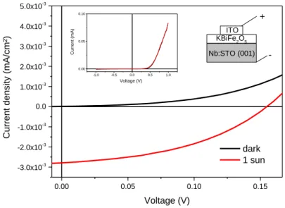
After having confirmed the structure and optical properties of the KBFO films, electrical properties were looked into. It was found that the in-plane resistivity or carrier properties could not be determined in the films grown on STO (001) or MAO (001) because they were found to be insulating. PFM measurements did not exhibit any sign of ferroelectricity or piezoelectricity with KBFO films grown on Nb-STO in order to have a conductive substrate. Such KBFO films on Nb-STO were found to be of better surface quality than with the STO substrate, with a root-mean-square roughness of 6 nm over 1 µm². The same KBFO on Nb-STO configuration was further covered with indium tin oxide (ITO) 1 mm² pads deposited by magnetron sputtering through a mask. A tungsten tip was applied on top of the pad and the backside was contacted with silver paste. Figure 5 shows the current-voltage characteristics obtained in dark and under 1 sun. The inset of Figure 5 shows that a rectifying behaviour is observed. When focussing on PV properties the short-circuit current density, open circuit voltage and fill factor were 2.8 µA/cm², 155 mV and 42% respectively. This short-circuit current density is about 5-7 times lower than references (12) and (13). It should be noted that the active area defined to convert the short-circuit current into a short-circuit current density has been taken as 1 mm², which is reasonable as the BFKO film is highly resistive and therefore the areas outside the ITO pad cannot contribute to the current. The power conversion efficiency is 1.8·10-4 %. While previous solar cells based on KBFO were obtained in bulk KBFO, here we demonstrate that similar performance in terms of short-circuit current density is obtained in KBFO thin films, which are more practical for possible applications. KBFO single crystal in Ref. (12) allowed a high Voc of 9.1 V
6 Nb-STO that provides multiple orientations of KBFO. The PV properties are low but encouraging because KBFO grown on Nb-STO did not provide epitaxy or high quality deposition. The short-circuit current remained the same after applying pulses of ±8 V between Nb-STO and ITO. This was expected because no ferroelectricity of KFBO films could be demonstrated. We attempted growing KBFO/SrRuO3//MAO (001) stacks. The aim was to obtain epitaxy of KBFO as in the case of
KBFO//MAO (001), but this time with a SrRuO3 conductive electrode instead of the electrode of
Nb-STO (001). However no peaks of SrRuO3 or KBFO could be observed by XRD. Alternative contact
materials on top and bottom of KBFO must therefore be investigated.
Conclusions
We attempted to grow KBFO by PLD and obtained epitaxial films, showing high quality deposition as evidenced by XRD and TEM. To our knowledge this is the first time that epitaxy of KBFO is obtained. Previous work on KBFO films obtained by sol-gel and spin coating were polycrystalline (15, 16). If the bandgap found of 2.2 eV is relatively high compared to the optimum for the solar spectrum for a single bandgap solar cell, the photoactive properties of KBFO have been clearly demonstrated which is a further step in polar functional materials. In order to further investigate the photovoltaic properties of the material, a suitable epitaxial conductive buffer layer on MAO (001) should be found in order to provide an electrode for KBFO. Our results are encouraging for future implementation of such oxide absorber in photovoltaic technology.
Supporting Information
Sketch showing epitaxial relationship, SEM images, SEM EDX analysis, low magnification TEM images, high magnification TEM images, TEM EDS mappings.
Acknowledgments
This research was carried out under the framework of the FERROPV project supported by the French Agence Nationale de la Recherche (ANR) under the reference ANR-16-CE05-0002-01. We thank S. Colis for ITO deposition, M. V. Rastei for PFM measurements. Han W. and H. W. acknowledge the support from the US Office of Naval Research (ONR, N00014-16-01-2465). The TEM work at Purdue University was supported by the U.S. National Science Foundation (NSF, DMR-1565822).
7
References
(1) Nechache, R.; Harnagea, C.; Li, S.; Cardenas L.; Huang, W.; Chakrabartty, J.; and Rosei, F. Bandgap tuning of multiferroic oxide solar cells. Nature Phot. 2015, 9, 61.
(2) Quattropani, A.; Makhort A.; Rastei, M.V.; Versini, G.; Schmerber, G.; Barre, S.; Dinia, A.; Slaoui, A.; Rehspringer, J.-L.; Fix, T.; Colis S. and Kundys, B. Tuning photovoltaic response in Bi2FeCrO6 films
by ferroelectric poling. Nanoscale 2018, 10, 13761.
(3) Quattropani A.; Stoeffler, D.; Fix, T.; Schmerber, G.; Lenertz, M.; Versini, G.; Rehspringer J. L.; Slaoui, A.; Dinia A. and Colis, S. Band-gap tuning in ferroelectric Bi2FeCrO6 double perovskite thin
films. Journal of Physical Chemistry C 2018, 122, 1070.
(4) Yuan, Y.; Xiao, Z.; Yang, B. and Huang, J. Arising applications of ferroelectric materials in photovoltaic devices. J. Mater. Chem. A 2014, 2, 6027.
(5) Paillard, C.; Bai, X.; Infante, I. C.; Guennou, M.; Geneste, G.; Alexe, M.; Kreisel, J.; Dkhil, B. Photovoltaics with Ferroelectrics: Current Status and Beyond. Adv. Mater. 2016, 28, 5153.
(6) Yang, S. Y.; Seidel, J.; Byrnes, S. J.; Shafer, P.; Yang, C. H.; Rossell, M. D.; Yu, P.; Chu, Y.-H.; Scott, J. F.; Ager, J. W.; Martin, L. W.; Ramesh, R. Above-bandgap voltages from ferroelectric photovoltaic devices. Nat. Nano. 2010, 5, 143.
(7) Basu, S. R.; Martin, L. W.; Chu, Y. H.; Gajek, M.; Ramesh, R.; Rai, R. C.; Xu, X. and Musfeldt J. L. Photoconductivity in BiFeO3 thin films. Appl. Phys. Lett. 2008, 92, 091905.
(8) Jellite, M.; Rehspringer, J.-L.; Fazio, M. A.; Muller, D.; Schmerber, G.; Ferblantier, G.; Colis, S.; Dinia, A.; Sugiyama, M.; Slaoui, A.; Cavalcoli, D.; Fix, T. Investigation of LaVO3 based compounds as a
photovoltaic absorber. Solar Energy 2018, 162, 1.
(9) Chakrabartty, J. P.; Nechache, R.; Harnagea, C. and Rosei, F. Photovoltaic effect in multiphase Bi-Mn-O thin films. Opt. Express 2014, 22, A80.
(10) Dimopoulos, T.; Peić, A.; Müllner, P.; Neuschitzer, M.; Resel, R.; Abermann, S.; Postl, M.; List, E. J. W.; Yakunin, S.; Heiss, W.; Brückl, H. Photovoltaic properties of thin film heterojunctions with cupric oxide absorber. J. Renew. Sustain. Energy 2013, 5, 011205.
8 (11) Kupfer, B.; Majhi, K.; Keller, D. A.; Bouhadana, Y.; Rühle, S.; Barad, H. N.; Anderson, A. Y.; Zaban, A. Thin Film Co3O4/TiO2 Heterojunction Solar Cells. Adv. Energy Mater. 2015, 5, 1401007.
(12) Zhang, G. ; Wu, H.; Li, G. ; Huang, Q. ; Yang, C. ; Huang, F. ; Liao, F. ; Lin, J. New high Tc
multiferroics KBiFe2O5 with narrow band gap and promising photovoltaic effect. Sci. Rep. 2016, 3,
1265.
(13) Jalaja, M. A.; Dutta, S. Switchable photovoltaic properties of multiferroic KBiFe2O5. Mater. Res. Bull. 2017, 88, 9.
(14) Zhang, M.; Wang, Z.; Lin, S.; Wang, Y.; Pan, Y. Investigation on a new multiferroic compound KBiFe2O5: Structural, optical, electrical and magnetic properties. J. Alloy Compd 2017, 699, 561.
(15) Zhai, X.; Deng, H.; Zhou, W.; Yang, P.; Chu, J.; Zheng, Z. Optical and magnetic properties of KBiFe2O5 thin films fabricated by chemical solution deposition. Mater. Lett. 2015, 161, 423.
(16) Jalaja, M. A.; Predeep, P. and Dutta, S. Ferroelectric, ferromagnetic and optical properties of KBiFe2O5 thin film: a structure property relationship. Mater. Res. Express 2017, 4, 016401.
(17) Mettout, B.; Tolédano, P.; Sombra, A. S. B.; Furtado Filho, A. F. G.; do Nascimento, J. P. C.; Santos da Silva M. A.; Gisse, P. and Vasseur, H. Magnetoelectric, photovoltaic, and magnetophotovoltaic effects in KBiFe2O5. Phys. Rev. B 2016, 93, 195123.
(18) Choi, E.-M.; Fix, T.; Kursumovic, A.; Kinane, C. J.; Arena, D.; Sahonta, S.-L.; Bi, Z.; Xiong, J.; Yan, L.; Lee, J.-S.; Wang, H.; Langridge, S.; Kim, Y.-M.; Borisevich, A. Y.; MacLaren, I. ; Ramasse, Q. M.; Blamire, M. G.; Jia, Q. and MacManus-Driscoll J. L. Room temperature Ferrimagnetism and Ferroelectricity in Strained, Thin Films of BiFe0.5Mn0.5O3. Adv. Funct. Mater. 2014, 24, 7478.
9 10 20 30 40 50 60 70 80 90 100 110 120 K B F O (0 7 0 ) ? K B F O (8 0 0 ) K B F O (0 2 0 ) K B F O (4 0 0 ) K B F O (0 4 0 ) S T O (0 0 4 ) S T O (0 0 3 ) S T O (0 0 2 )
Counts (
a. u.)
2
(deg.)
S T O (0 0 1 ) 10 20 30 40 50 60 70 80 90 100 110 120 K B F O (8 0 0 ) K B F O (4 0 0 ) M A O (0 0 8 ) M A O (0 0 4 )Counts (
a. u.)
2
(deg.)
Figure 1: XRD θ–2θ pattern of a 60 nm thick KBFO thin film grown on STO (001) (a) and MAO (001)
(b) substrates.a)
10 600 800 1000 1200 1400 0 1000 2000 O K Fe RBS yield (a .u. ) Energy (keV) Bi
11 Figure 3: TEM of KBFO film on MAO (001) in the MAO [010] zone axis: a) low-magnification TEM image, b) selected area diffraction patterns (SAED) of thin film and substrate, and c) high-magnification TEM image, d) EDS mapping showing Bi, Fe and Mg.
MAO (004) KBFO (400)
[001]
[010]
[400]
[012]
12 400 600 800 1000 1200 0.0 0.1 0.2 0.3 0.4 0.5 1 2 3 4 0 1x10¹⁵ 2x10¹⁵ 3x10¹⁵ ( E)² Energy (eV) KBiFe2O5 60 nm//MAO(001) MAO(001)
Wavelength (nm)
Optical absorptio
n (a. u.
)
Figure 4: Optical absorption vs. wavelength of a 60 nm thick KBFO thin film on MAO (001). Inset: the Tauc plot for the same sample for a direct bandgap.
0.00 0.05 0.10 0.15 -3.0x10⁻³ -2.0x10⁻³ -1.0x10⁻³ 0.0 1.0x10⁻³ 2.0x10⁻³ 3.0x10⁻³ 4.0x10⁻³ 5.0x10⁻³ -1.0 -0.5 0.0 0.5 1.0 0.00 0.05 0.10 Curr en t d en sity (m A/cm²) Voltage (V) dark 1 sun -Nb:STO (001) KBiFe2O5 ITO + Current (mA) Voltage (V)