Conformal single-layer encapsulation
of PEDOT at low substrate temperature
The MIT Faculty has made this article openly available. Please share how this access benefits you. Your story matters.Citation Chen, Nan, Xiaoxue Wang, and Karen K. Gleason. “Conformal
Single-Layer Encapsulation of PEDOT at Low Substrate
Temperature.” Applied Surface Science 323 (December 2014): 2-6.
As Published http://dx.doi.org/10.1016/j.apsusc.2014.06.123
Publisher Elsevier
Version Author's final manuscript
Citable link http://hdl.handle.net/1721.1/106566
Terms of Use Creative Commons Attribution-NonCommercial-NoDerivs License
Conformal Single-layer Encapsulation of PEDOT at Low Substrate
Temperature
Nan Chen, Xiaoxue Wang, Karen K. Gleason*
Department of Chemical Engineering, Massachusetts Institute of Technology, Cambridge, MA 02139
Corresponding Author
*E-mail address: [email protected]
Abstract
In this work, we demonstrate a single-layer encapsulation method for poly(3,4-ethylenedioxythiophene) (PEDOT). This method is achieved by initiated chemical vapor deposition (iCVD) process, which is scalable and employs solvent-free and low-substrate temperature conditions. The encapsulant used, poly(divinylbenzene-co-maleic anhydride) (PDVB-MA), was first time synthesized via vapor phase process. This cross-linked iCVD polymer can be rapidly deposited (40 nm min-1) with uniform and conformal morphology. In the test of PEDOT degradation, the encapsulation extended the halflife of PEDOT to 900 hours at 30°C in air, which is more than ten times of the counterpart without encapsulation.
Keywords
1. Introduction
Conducting polymers are rapidly developing as electromaterials used in organic solar cells, organic light-emitting diodes (OLEDs), and biomedical applications.[1-6] They are attractive due to their easy processing, flexibility, low cost and high porosity, which is important for many commercial applications. Among all organic conducting materials, PEDOT has shown a great promise as a result of its high conductivities (>1000 S cm-1).[7, 8] However, like many organic materials in this field, PEDOT is chemically unstable. The instability of PEDOT, which limits its application in industry, registers as the deterioration of its electrical conductivity in air.[9-12] Thus, there is great need to improve the stability of PEDOT. PEDOT in air can undergo multiple degradation mechanisms. Previous studies indicated oxidization by permeated oxygen can decrease the conductivity of PEDOT,[10] and water vapor adsorption resulted insulating patches may also increase the resistivity of PEDOT.[13] At elevated temperature, thermal shrinkage of the conducting area can also cause conductivity loss of PEDOT.[9] Last but not least, scientists found sizes of dopant molecules in PEDOT films have a large impact on its conductivity loss, which suggests that a loss of dopants is also a mechanism of PEDOT degradation.[14, 15] Previous reports indicated that acid-rinsed PEDOT has enhanced stability as well as increased conductivity as the removal of the excess hygroscopic oxidant and improved chain packing, which provides a better barrier for oxygen and moisture.[15] However, the acid-rinse cannot prevent escape of dopants, although it can reduce the degradation caused by permeated oxygen or water vapor. Therefore, a cross-linked network preventing loss of dopants may be an efficient way to encapsulate and enhance the stability of acid-rinsed PEDOT.
Previous achievements on the encapsulation of PEDOT and its copolymers include parylene[16, 17], silicon nitride[4], and et al.. These materials have been proved to provide excellent barrier to water vapor and oxygen. However, there is still a need of a solvent-free and low-temperature encapsulation method, which is simple to apply and easy to scale up, since PEDOT applications are usually sensitive to heat, solvent, and plasma. iCVD is a solvent-free deposition method for conformal and functional polymer thin films. In this process, monomer and initiator flow into a vacuum chamber, passing through a hot filament, where initiators get thermally activated. On a cooled substrate beneath the filament, adsorbed monomers and radicals from activated initiator react and form a uniform layer of polymer thin film. In iCVD, thermal activation and polymerization happened on different sites, so the temperature of substrate can stay cool, and functional groups of the monomer can be retained. Films deposited via iCVD polymerization are highly conformal and uniform.[18-21] Moreover, the iCVD process is scalable and easily integrated with other techniques, such as roll-to-roll processing[22] and plasma enhanced CVD[23]. These unique advantages make it an ideal way of encapsulation.
2. Material and Method 2.1 PEDOT synthesis
PEDOT was deposited directly on glass substrates via an oxidative chemical vapor deposition process (oCVD) described elsewhere.[15, 20] Here, we only summarize key details. 3,4-ethylenedioxythiophene (EDOT, Aldrich 97%) vapors was delivered to vacuum chamber at flow rate of ~5 sccm. FeCl3 oxidant (Sigma Aldrich, 99.99%) was
1.5 °C min-1. Glass substrates at a substrate temperature of 150 °C were exposed to monomer and oxidant under the chamber pressure of 10-4 Torr for 40 minutes. After synthesis, PEDOT samples were rinsed by hydrobromic acid (HBr, Aldrich 48%, diluted with deionized H2O to 5 mol L-1) for 5 minutes then followed by drying for 30 minutes
before a final rinse with methanol. All rinsing steps were done in ambient conditions. Two 4mm-wide strips of silver (Alfa Aesar, 1~3 mm particles, 99.9999%) were thermally evaporated onto edges of PEDOT film in order to avoid damage to encapsulation layer during measurements of resistance. The resistance (R) of PEDOT samples was measured by a multimeter (Keithley, model 2000, 4-wire mode), and then converted to conductivity (C) using Eq. 1.
𝐶 =𝑅×𝑊×𝑇𝐿 (1)
where L, W, and T represent length, width and thickness of PEDOT film, respectively.
2.2 Encapsulation
The PDVB-MA thin film was deposited directly on top of the PEDOT film at a rate of 20~40 nm min-1 using the iCVD process described elsewhere.[21] We only summarize key details in here. The deposition pressures (0.27 Torr and 0.67 Torr) were maintained using a throttling butterfly valve. The substrate temperature was controlled at 25 °C. Two monomers, divinylbenzene (DVB, Sigma Aldrich, 80%) and maleic anhydride (MA, Sigma Aldrich, 99%) were heated at 60 and 80 °C, respectively. Monomers were delivered into the chamber at ~1.0 sccm controlled by needle valves. The initiator, tert-butyl peroxide (TBPO, Sigma Aldrich 98%), was delivered by a mass flow controller (MKS Instruments, model 1479) at ~1.0 sccm under room temperature.
The filament array (Chromaloy O resistance alloy, Goodfellow) was heated to 270 °C in order to activate the initiator. An in-situ interferometry (JDS Uniphase, 633 nm HeNe laser) was used to monitor the film growth. Thicknesses of deposited PDVB-MA films were measured on bare silicon wafers (Wafer World, Inc., aside of PEDOT samples in the reactor) by a variable angle spectroscopic ellipsometer (VASE, J. A. Woollam M-2000) at incident angles of 65°, 70°, and 75°. Fourier transform infrared (FTIR) spectrum was measured by Thermo Nicolet Nexus 870 spectrometer. Morphology of films was investigated by scanning electron microscope (SEM, JEOL 6010L) and atomic force microscopy (AFM, Digital Instruments, model D3100). Root–mean–square (RMS) roughness of films was measured on a 5 μm × 5 μm surface area using AFM.
3. Results and Discussion
3.1 Characterization of PDVB-MA
We use FTIR spectrum to confirm the structure of the synthesized copolymer. In Fig. 1, strong absorptions at 1780 and 1870 cm−1 are due to stretching of carbonyl groups from the 5-member ring of maleic anhydride.[24]. Absence of strong absorption at 903 cm-1 indicates vinyl groups from DVB were reacted during the polymerization.[25] Absorptions around 2900 cm−1 are from symmetric and asymmetric C-H stretching in the backbone of the newly formed polymer chain of PDVB-MA.[26, 27]
Cross-linked polymer networks are useful in many applications, including but not limited to sensors, micro-fluidic devices, shape memory films, and electronics protection.[28-30] PDVB and its copolymers have been used in many applications of cross-linked networks.[31-33] Previous report indicated copolymerization of styrene and MA has much faster deposition rate than that of polystyrene homopolymer.[34] Similar
results were observed in copolymerization of DVB and MA. Compared to the deposition rate of PDVB homopolymer in iCVD process (~4 nm min-1), the PDVB-MA copolymer shows a rapid deposition rate (up to 40 nm min-1). This higher deposition rate would correspond to lower overall cost. In order to clearly show the role of MA in accelerating the deposition, it is necessary to define a fundamental characteristic of the iCVD process, PM / Psat, which is the ratio of the partial pressure of monomer to its saturation vapor
pressure at certain substrate temperature. This ratio is directly related to the equilibrium surface concentration of adsorbed monomers based on Brunauer, Emmett, and Teller (BET) isotherm.[35] Previous report indicated 0.4~0.7 is an optimal PM / Psat range for
rapid iCVD processes of vinyl monomers.[36] We summarize deposition rate of PDVB-MA at different PM / Psat of MA in Fig. 2. In the range of 0~0.7, PM / Psat of MA shows
linear relationship with the deposition rate of the copolymer, which indicates participation of MA accelerated the reaction. In our experiments, the fastest deposition rates (40 nm min-1) occurred at PM / Psat = 0.7. Based on following BET equations[37, 38]
(Eq. 2 and Eq. 3), we can estimate an adsorption energy of 24.8 kJ mol-1, which is in the typical range of 20 to 80 kJ mol-1 for physisorption of small molecules.[39]
𝑉𝑎𝑑 = 𝑉𝑚𝑙𝐶(𝑃𝑀/𝑃𝑆𝐴𝑇)
(1−𝑃𝑀/𝑃𝑆𝐴𝑇)[1−(1−𝐶)(𝑃𝑀/𝑃𝑆𝐴𝑇)] (2) 𝐶 = exp(𝐸𝑎𝑑
𝑅𝑇) (3)
where Vad, Vml, C, and Ead represent adsorbed volume, monolayer adsorbed volume, the
BET constant, and adsorption energy, respectively. Besides the effect of PM / Psat,
temperatures of the filament (Tf) can also affect the deposition rate in the synthesis of
PDVB-MA. Previous publication indicates the degree of decomposition of TBPO increases as Tf increases when Tf < 270 °C, and higher Tf results methyl radicals[40],
which is more reactive than the tert-butoxy radicals and therefore accelerate the free-radical polymerization.[41]
3.2 Conformality, uniformity, and surface roughness
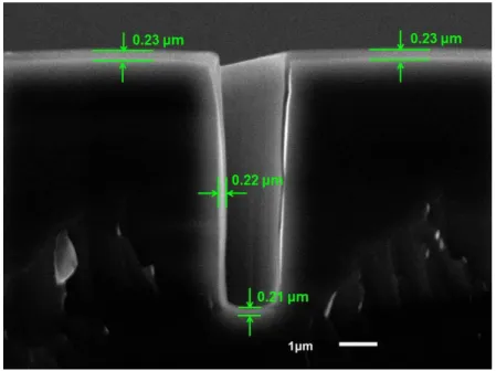
Describing the ability to encapsulate the entire surface topography, conformality is an important standard to judge an encapsulation method. Conformal coating is highly desired since it can bring additional functionalities without changing the original morphology, which is important in many micro fabrication steps. In this work, we use cross-sectional SEM to demonstrate the overall profiles for PDVB-MA films rapidly growing (35 nm min-1) inside a trench feature (aspect ratio = 4.2). Fig. 3 shows good thickness uniformity over the entire trench feature, which indicates the conformal nature of iCVD synthesized PDVB-MA films. Another important parameter of thin film coating is the uniformity of entire coating area. In order to demonstrate this uniformity, we deposited 350 nm PDVB-MA film on a bare silicon substrate and measured thicknesses at different positions in a 8 × 8 cm area by VASE. In Table 1, thicknesses at five different positions in the area are all within 5% of the averaged thickness, which indicates the iCVD deposition of PDVB-MA is uniform all over the entire 8 × 8 cm area. AFM is also used to characterize the surface morphology. Fig. 4 a) shows the AFM image of the bare acid-rinsed PEDOT, and Fig. 4 b) shows the same sample encapsulated with 200 nm PDVB-MA thin film. The RMS surface roughness calculated from a 5 × 5 μm area dropped from 2.35 nm before encapsulation to 0.63 nm after encapsulation. The reduced roughness suggests the PDVB-MA encapsulation smoothed the surface, which helps to reduce the absorption of water and oxygen.
3.3 PEDOT degradation
We tested the stability of PEDOT with and without encapsulation in air at 30°C. In order to characterize the performance of encapsulation, we define the time when PEDOT lose half of its original conductivity as its halflife. In Fig. 5, the PEDOT sample without encapsulation shows a halflife of 118 hours. With PDVB-MA encapsulation, the halflife of PEDOT can be extended to more than 850 hours, which is a 7-fold increase. We observed encapsulation with PDVB-MA films with different thicknesses, but we did not observe any obvious effect of thickness in the range of 200 nm to 800 nm, and a 4-fold increase in encapsulate thickness only brings less than 5% increase of the halflife. This suggests that the 200 nm film of PDVB-MA is sufficient to prevent loss of dopants, which is considered as one of major degradation mechanisms of acid-rinsed PEDOT. Also, the shape of curves in Fig. 5 indicates at least two mechanisms were involved in the degradation of PEDOT as the flat stage shown between 0 to 170 hours. However, it is still not enough to make a clear conclusion on the role of different mechanisms in PEDOT degradation. Further experiments are being carrying out to address this issue.
4. Conclusion
We have successfully synthesized PDVB-MA via iCVD process for the first time. This cross-linked polymer performs as a good single-layer encapsulant for PEDOT, and extends the halflife of PEDOT to 900 hours at 30°C in air. The rapid encapsulation method features with solvent-free and low-substrate-temperature conditions, which is ideal for many fragile PEDOT applications. The effect of monomer saturation ratio on the deposition rate is discussed, and a deposition rate of 40 nm min-1 was achieved at PM / Psat
(MA) = 0.7. For morphology of the deposited films, SEM, VASE, and AFM investigations indicate the iCVD PDVB-MA film is conformal, uniform, and smooth, respectively. Overall, iCVD is an ideal method for conformal, solvent-free encapsulations at low substrate temperature.
Acknowledgement
The authors thank for the financial supports by Eni S.p.A. under the ENI-MIT Solar Frontier Center.
Reference
[1] B.L. Groenendaal, F. Jonas, D. Freitag, H. Pielartzik, J.R. Reynolds,
Poly(3,4-ethylenedioxythiophene) and its derivatives: Past, present, and future, Advanced Materials, 12 (2000) 481-494.
[2] H.W. Heuer, R. Wehrmann, S. Kirchmeyer, Electrochromic window based on conducting
poly (3,4-ethylenedioxythiophene)poly(styrene sulfonate), Advanced Functional Materials, 12 (2002) 89-94.
[3] S. Kirchmeyer, K. Reuter, J.C. Simpson, Poly(3,4-ethylenedioxythiophene) - scientific
importance, remarkable properties, and applications, 3rd ed., CRC Press, New York, NY,
2007.
[4] B. Charlot, G. Sassine, A. Garraud, B. Sorli, A. Giani, P. Combette, Micropatterning
PEDOT:PSS layers, Microsystem Technologies-Micro-and Nanosystems-Information Storage
[5] G.G. Wallace, S.E. Moulton, R.M.I. Kapsa, M.J. Higgins, Organic Conducting Polymers, in:
Organic Bionics, Wiley-VCH, Weinheim, 2012, pp. 81-112.
[6] W. Lu, J. Kuwabara, T. Iijima, H. Higashimura, H. Hayashi, T. Kanbara, Synthesis of
pi-Conjugated Polymers Containing Fluorinated Arylene Units via Direct Arylation: Efficient
Synthetic Method of Materials for OLEDs, Macromolecules, 45 (2012) 4128-4133.
[7] M.V. Fabretto, D.R. Evans, M. Mueller, K. Zuber, P. Hojati-Talemi, R.D. Short, G.G. Wallace,
P.J. Murphy, Polymeric Material with Metal-Like Conductivity for Next Generation Organic
Electronic Devices, Chemistry of Materials, 24 (2012) 3998-4003.
[8] D. Evans, M. Fabretto, M. Mueller, K. Zuber, R. Short, P. Murphy, Structure-directed
growth of high conductivity PEDOT from liquid-like oxidant layers during vacuum vapor
phase polymerization, Journal of Materials Chemistry, 22 (2012) 14889-14895.
[9] E. Vitoratos, S. Sakkopoulos, E. Dalas, N. Paliatsas, D. Karageorgopoulos, F. Petraki, S. Kennou, S.A. Choulis, Thermal degradation mechanisms of PEDOT:PSS, Organic Electronics,
10 (2009) 61-66.
[10] K. Norrman, M.V. Madsen, S.A. Gevorgyan, F.C. Krebs, Degradation Patterns in Water and Oxygen of an Inverted Polymer Solar Cell, Journal of the American Chemical Society,
132 (2010) 16883-16892.
[11] S. Sarkar, J.H. Culp, J.T. Whyland, M. Garvan, V. Misra, Encapsulation of organic solar cells with ultrathin barrier layers deposited by ozone-based atomic layer deposition,
Organic Electronics, 11 (2010) 1896-1900.
[12] H.J. Lee, H.P. Kim, H.M. Kim, J.H. Youn, D.H. Nam, Y.G. Lee, J.G. Lee, A.B. Yusoff, J. Jang,
Solution processed encapsulation for organic photovoltaics, Solar Energy Materials and Solar Cells, 111 (2013) 97-101.
[13] K. Kawano, R. Pacios, D. Poplavskyy, J. Nelson, D.D.C. Bradley, J.R. Durrant, Degradation
of organic solar cells due to air exposure, Solar Energy Materials and Solar Cells, 90 (2006) 3520-3530.
[14] H. Chelawat, S. Vaddiraju, K. Gleason, Conformal, Conducting
Poly(3,4-ethylenedioxythiophene) Thin Films Deposited Using Bromine as the Oxidant in a
Completely Dry Oxidative Chemical Vapor Deposition Process, Chemistry of Materials, 22
(2010) 2864-2868.
[15] R.M. Howden, E.D. McVay, K.K. Gleason, oCVD poly(3,4-ethylenedioxythiophene) conductivity and lifetime enhancement via acid rinse dopant exchange, Journal of Materials
Chemistry A, 1 (2013) 1334-1340.
[16] D. Khodagholy, T. Doublet, M. Gurfinkel, P. Quilichini, E. Ismailova, P. Leleux, T. Herve, S.
Sanaur, C. Bernard, G.G. Malliaras, Highly Conformable Conducting Polymer Electrodes for In Vivo Recordings, Advanced Materials, 23 (2011) H268-+.
[17] S. Takamatsu, T. Takahata, K. Matsumoto, I. Shimoyama, Micro-patterning of a
conductive polymer and an insulation polymer using the Parylene lift-off method for electrochromic displays, Journal of Micromechanics and Microengineering, 21 (2011).
[18] M.L. Ma, Y. Mao, M. Gupta, K.K. Gleason, G.C. Rutledge, Superhydrophobic fabrics
produced by electrospinning and chemical vapor deposition, Macromolecules, 38 (2005) 9742-9748.
[19] C.T. Riche, B.C. Marin, N. Malmstadt, M. Gupta, Vapor deposition of cross-linked
fluoropolymer barrier coatings onto pre-assembled microfluidic devices, Lab on a Chip, 11
(2011) 3049-3052.
[20] J.J. Xu, K.K. Gleason, Conformal Polymeric Thin Films by Low-Temperature Rapid
Initiated Chemical Vapor Deposition (iCVD) Using tert-Butyl Peroxybenzoate as an Initiator,
[21] M. Karaman, N. Cabuk, D. Ozyurt, O. Koysuren, Self-supporting superhydrophobic thin
polymer sheets that mimic the nature's petal effect, Applied Surface Science, 259 (2012) 542-546.
[22] M. Gupta, K.K. Gleason, Large-scale initiated chemical vapor deposition of poly(glycidyl
methacrylate) thin films, Thin Solid Films, 515 (2006) 1579-1584.
[23] A.M. Coclite, G. Ozaydin-Ince, F. Palumbo, A. Milella, K.K. Gleason, Single-Chamber
Deposition of Multi layer Barriers by Plasma Enhanced and Initiated Chemical Vapor
Deposition of Organosilicones, Plasma Processes and Polymers, 7 (2010) 561-570.
[24] D. Lin-Vien, The Handbook of infrared and raman characteristic frequencies of organic
molecules / Daimay Lin-Vien ... [et al.], Boston : Academic Press, c1991., 1991.
[25] C.D. Petruczok, R. Yang, K.K. Gleason, Controllable Cross-Linking of Vapor-Deposited
Polymer Thin Films and Impact on Material Properties, Macromolecules, 46 (2013) 1832-1840.
[26] K.M. McNamara, B.E. Williams, K.K. Gleason, B.E. Scruggs, Identification of Defects and
Impurities in Chemical-Vapor-Deposited Diamond Through Infrared-Spectroscopy, Journal of Applied Physics, 76 (1994) 2466-2472.
[27] C.Y. Chen, C.L. Loch, J. Wang, Z. Chen, Different molecular structures at polymer/silane
interfaces detected by SFG, Journal of Physical Chemistry B, 107 (2003) 10440-10445. [28] G.H. Seong, W. Zhan, R.M. Crooks, Fabrication of microchambers defined by
photopolymerized hydrogels and weirs within microfluidic systems: Application to DNA
hybridization, Analytical Chemistry, 74 (2002) 3372-3377.
[29] A. Richter, G. Paschew, S. Klatt, J. Lienig, K.-F. Arndt, H.-J.P. Adler, Review on hydrogel-based pH sensors and microsensors, Sensors, 8 (2008) 561-581.
[30] A. Hatch, G. Hansmann, S.K. Murthy, Engineered Alginate Hydrogels for Effective
Microfluidic Capture and Release of Endothelial Progenitor Cells from Whole Blood, Langmuir, 27 (2011) 4257-4264.
[31] R. Yang, H. Jang, R. Stocker, K.K. Gleason, Synergistic Prevention of Biofouling in
Seawater Desalination by Zwitterionic Surfaces and Low-Level Chlorination, Adv. Mater., 26 (2014) 1711–1718.
[32] A.T. Paxson, J.L. Yagüe, K.K. Gleason, K.K. Varanasi, Stable Dropwise Condensation for
Enhancing Heat Transfer via the Initiated Chemical Vapor Deposition (iCVD) of Grafted Polymer Films, Advanced Materials, 26 (2014) 418-423.
[33] A. Asatekin, K.K. Gleason, Polymeric Nanopore Membranes for Hydrophobicity-Based
Separations by Conformal Initiated Chemical Vapor Deposition, Nano Letters, 11 (2011)
677-686.
[34] W.E. Tenhaeff, K.K. Gleason, Initiated chemical vapor deposition of perfectly alternating
poly(styrene-alt-maleic anhydride), Surface & Coatings Technology, 201 (2007) 9417-9421.
[35] S. Brunauer, P.H. Emmett, E. Teller, Adsorption of gases in multimolecular layers, Journal of the American Chemical Society, 60 (1938) 309-319.
[36] K.K.S. Lau, K.K. Gleason, Initiated chemical vapor deposition (iCVD) of poly( alkyl
acrylates): An experimental study, Macromolecules, 39 (2006) 3688-3694.
[37] P. Atkins, J. de Paula, Physical Chemistry, 7th ed., W. H. Freeman & Co., New York, 2002.
[38] K.K.S. Lau, K.K. Gleason, Initiated chemical vapor deposition (iCVD) of poly(alkyl
acrylates): A kinetic model, Macromolecules, 39 (2006) 3695-3703.
[39] D.O. Hayword, B.M.W. Trapnell, Chemisorption, 2nd ed., Butterworths, London, 1968. [40] P.G. Mekarbane, B.J. Tabner, Interaction between radicals derived from two di-t-alkyl
[41] A.M. Coclite, Y. Shi, K.K. Gleason, Controlling the Degree of Crystallinity and Preferred
Crystallographic Orientation in Poly-Perfluorodecylacrylate Thin Films by Initiated
Figure 1. FTIR spectrum of 200nm PDVB-MA film on silicon substrate. The insert panel shows the structure diagram of PDVB-MA.
O O O
Figure 2. Effect of PM / Psat (MA) on the rate of deposition at Tsubstrate = 25°C and Tfilament
= 270°C. Error bars on data points are standard deviations observed in replicate measurements. The trendline is a linear fit of all data points.
Figure 4. AFM images of a) PEDOT on a silicon substrate; b) 200 nm PDVB-MA encapsulated PEDOT on silicon substrate.