HAL Id: hal-02088188
https://hal.laas.fr/hal-02088188
Submitted on 2 Apr 2019
HAL is a multi-disciplinary open access
archive for the deposit and dissemination of
sci-entific research documents, whether they are
pub-lished or not. The documents may come from
teaching and research institutions in France or
abroad, or from public or private research centers.
L’archive ouverte pluridisciplinaire HAL, est
destinée au dépôt et à la diffusion de documents
scientifiques de niveau recherche, publiés ou non,
émanant des établissements d’enseignement et de
recherche français ou étrangers, des laboratoires
publics ou privés.
Gate Defects Analysis in AlGaN/GaN Devices by Mean
of Accurate Extraction of the Schottky Barrier Height,
Electrical Modeling, T-CAD Simulations and TEM
Imaging
Jean-Guy Tartarin, Oana Lazar, Damien Saugnon, B Lambert, C Moreau, C
Bouexiere, E Romain-Latu, K Rousseau, A David, J.L. Roux
To cite this version:
Jean-Guy Tartarin, Oana Lazar, Damien Saugnon, B Lambert, C Moreau, et al.. Gate Defects
Analysis in AlGaN/GaN Devices by Mean of Accurate Extraction of the Schottky Barrier Height,
Electrical Modeling, T-CAD Simulations and TEM Imaging. 28th European Symposium on Reliability
of Electron Devices, Failure Physics and Analysis (ESREF 2017), Sep 2017, Bordeaux, France.
�hal-02088188�
Gate Defects Analysis in AlGaN/GaN Devices by Mean of Accurate
Extraction of the Schottky Barrier Height, Electrical Modeling,
T-CAD Simulations and TEM Imaging
J.G. Tartarin
a,*, O. Lazar
a, D. Saugnon
a, B. Lambert
b, C. Moreau
c, C. Bouexiere
c,
E. Romain-Latu
d, K. Rousseau
d, A. David
e, J.L. Roux
f
1. Introduction
ALGAN/GAN HEMTS are already known for their
outstanding performances in microwave field of applications. The high breakdown voltage, electron saturation velocity, cutoff frequency and figures of merit, reveal them as attractive competitors towards the classical solid state transistors developed on silicon and GaAs materials. Using GaN for electronic circuits results in a loss in weight for the system (reduction in the electronic circuit area, power supply and heater or cooling system sizes), with enhanced power capabilities. Yet, limitations like the increase of the junction temperature still represent a challenge to broaden the application fields and markets. Systems working at elevated junction temperature can open the way for new high power and high frequency applications, as for example large volume production dedicated to base stations and other high volume markets, but also to defense and space purposes working under harsh environment. However, reliability investigations are still largely under concern because of the complex electro-thermo-mechanical mechanisms induced in transistors; these reliability studies can only be carried out by using several cross-experiments, or by using destructive techniques in order to evidence the presence of defects. Nevertheless, destructive techniques do not allow concluding about the real impact of the revealed defect on the electrical behavior of the device. The development of new non-invasive (and then non-destructive) experimental approaches can thus bring information about the evolution of electrical signatures before (during) and after application of a stress. This study specifically focuses
on gate barrier height related defects, as it impacts the control of the charges in the channel where the electron carriers flow, and interface states causing various reliability issues. Devices were tested under High Temperature Operating Life stress conditions (HTOL). T-CAD model is also developed to account for the fine technological mechanism analysis of the gate control zone, as well as interface fixed charge densities effects on static electrical parameters.
This document is structured as follows: the second section briefly describes the technology under test and the stress conditions used on a sample of 10 devices. The third section is dedicated to the extraction method of the Schottky Barrier Height (SBH) and associated electrical models as well as T-CAD simulations. The last section deals with TEM pictures at the gate edges and under the gate. Lastly, a conclusion is drawn which states the usefulness of the proposed method in terms of technological feedback.
2. Technology under test and under stress
Results on an intermediate step of the final technological declination (under development phase) are reported, with the aim to assess the potential of our method. A batch of ten AlGaN/GaN HEMT devices featuring eight gate fingers, with a width of 125 µm each (technology 0.25 µm gate length), grown on SiC substrate have been used for the study. Two virgin devices are available to evaluate the impact of the HTOL stress operated by UMS at VDS=30V and
IDS=100mA/mm ,at 175°C ambient temperature (320°C
peak junction temperature extracted from simulation model). The measurements reveal a drop on IDS of
about 45% (at VGS = 1 V and VDS = 8 V), an increase of
130% on RON, and about one decade variation on IGS
after 105 hours of HTOL stress. Threshold voltage relative evolutions during the stress are reported in Fig. 1, with final shifts between 5% and 15% on stressed devices (no variation on the two virgin devices also measured – black and red plots).
The demand of having a clean gate contact in power devices is still a key challenge in achieving reliable processes, since some of the failure mechanisms are related to the specific development of the Schottky gate contact. Moreover, the gate terminal (i.e., the command) is the critical zone impacting the performances of the device: shift of the threshold voltage Vth, leads to variation of the transconductance
gain and of the carriers’ density in the two-dimensional electron gas, which become detrimental to the circuit operation and to the system performances.
3. Electrical measurements and modelling of the Gate Schottky Diode
From previous studies [1]–[3], different methods have been developed to investigate the gate contact. Since we are talking about diodes and non-destructive techniques, the most common approach consists in the analysis of the SBH. This part of the work is based on prior studies [4][5], which present an accurate tool for extracting the SBH alone, through the quantification of the defects impact on the global SBH. The technique from [5] brings information about a mean SBH 𝛷𝐵𝑥
and its relative dispersion 𝜎𝑆𝑥 (inhomogeneity of the
barrier, Fig. 2). This technique is non-invasive as it is based on electro-thermal characterization of the device, in open drain configuration (no dissipated power in the
2DEG). Fig. 3 plots the gate current versus the gate voltage for a virgin device V#6 (Fig. 3.a) and for a
stressed device S#2 (Fig. 3.b) at different temperatures.
Fig. 4 gives the thermal evolution of the SBH expressed according to its classical electrical expression. Two thermal trends from part of a thermal inflexion point are observed.
a)
b)
Fig. 3. IGS-VGS measurements versus temperature, with a
25 K step for: a) V#6 (virgin sample) and b) S#2 (stressed
sample). Light grey is represented as the lowest temperature, towards dark black as the highest temperature.
Fig. 2. Representation of the parameters from Werner’s method applied to Richardson's model as expressed in [5]: a constant mean value of the SBH (𝛷𝐵𝑥) and an associated
standard deviation (±𝜎𝑆𝑥), i.e. a mathematical expression
for the SBH’s inhomogeneity.
Fig. 1. Impact of the HTOL stress on threshold voltage shift (expressed in percentage).
3.1. Extraction of the mean SBH and dispersion – extracting the accurate ideal SBH
From [5], the determination of the mean SBH and a related dispersion (𝛷𝐵𝑥, 𝜎𝑆𝑥) is found not to be
sufficient to get the Schottky Barrier Height determined accurately. By varying the IGS current range
(considering a 2-decades window) or by changing the temperature, it is demonstrated that:
-the mean SBH evolves largely out of the uncertainty zone of the method, and depends on the IGS range,
-the trend of the mean SBH also depends on the temperature window (next called High Temperature and Low Temperature zones) as depicted in Fig.4.
Concerning the extraction’s accuracy of the mean SBH associated to the method proposed in [5], it has been established that:
-errors due to signal analyzer measurements can be considered insignificant
-an error of less than 7% on 𝛷𝐵𝑥 is obtained for 50%
variation on prerequisite initial conditions on Richardson constant A* and effective mass m*.
-the larger variation is noticed when considering the standard deviation associated to the extracted SBH 𝛷𝐵𝑥 for each ‘x’ sliding window of IGS (Fig. 5). From
a dedicated study, it has been established that two decades window for IGS features the lowest variations.
An original reinterpretation of the pairs (𝛷𝐵𝑥, 𝜎𝑆𝑥)
has been proposed in [5] by plotting 𝛷𝐵𝑥 versus 𝜎𝑆𝑥
for all the ‘x’ sliding windows of two decades of IGS
(Fig. 6 a and b). Therefore, the variation of the mean SBH versus the standard deviation (inhomogeneity) represents the sensitivity of the ideal SBH’s value to the defects of the barrier height (inhomogeneity at the metal-semiconductor interface). Thus, the x-axis extrapolation at S = 0 eV represents the ideal Schottky
diode without considering any defect (B-s=0; expected
theoretical homogeneous SBH).
a)
b)
Fig. 6. Variations of 𝛷𝐵𝑥 versus 𝜎𝑆𝑥 under different gate
current ranges (x-sliding gate current window), for: a) S#2
(stressed device #2), and b) S#19 (stressed sample #19).
Squares represent the pairs (𝛷𝐵𝑥, 𝜎𝑆𝑥) in the low
temperature range and circles are the pairs (𝛷𝐵𝑥, 𝜎𝑆𝑥) in the
high temperature range. Fig. 5. Example for the extracted mean 𝛷𝐵𝑥 against the ‘x’
sliding window (2 decades IGS), considering the variation
of the standard deviation 𝜎𝑆𝑥, vertical error bars
(illustration on virgin device #6).
0 0.3 0.6 0.9 1.2 1.5 0 1 2 3 4 5 6 ɸB (e V ) 1000/T (K-1) Sample V#6 high T° low T° 0 0.5 1 1.5 0 5 10 ɸB (e V ) 1000/T (K-1) Sample S#2 high T° low T°
Fig. 4. SBH extracted from classical expression versus temperature for a virgin device V#6 and for a stressed
device S#2. An inflexion point separates two temperature
The different trends revealed at low or high temperature in Fig. 6.a and Fig. 6.b are consistent with first order and second order defects of the Schottky diode: however, whatever the increasing (stressed devices) or decreasing (virgin devices) impact of the defect within the high temperature window (see Fig.7), a unique B-s=0 is extracted at 1.1eV (±0.1eV).
For the lower temperature range, some devices still exhibit an extrapolation of B-s=0 at 1.1eV while two
devices give an extrapolation at 0eV (see Fig. 6.b, blue squares). This behavior correlates with Energy Dispersive X-Ray spectrometry (EDX) measurements, evidencing a gold conduction path at the edge of the gate as previously shown in [6].
3.2. Electrical models of the gate diode versus temperature
Electrical model has been developed and tuned for all temperatures under study and for all devices under
test, revealing different zones in forward biasing conditions that correlate the results from the previous section (TE mode). Fig. 8 reports IGS-VGS plot at 150K
where a second diode is identified at medium IGS, but
with higher serial resistor (revealing a conduction path not flowing into the quantum well). A highly resistive behaviour is also revealed (ranging from 108 to 1012)
at low IGS attributed to leakage current at the interface
between the SiN passivation and the AlGaN layer (no Schottky diode is involved in this electrical path). This resistive behaviour is reported for 5 devices under test in Fig. 9 (4 devices featuring 4.109as illustrated in
the inset, and 1 virgin device featuring a higher 1012
resistance). The measurements are reproducible.
3.3. T-CAD models
T-CAD simulator (Sentaurus) has been instructed and tuned to match both the stressed and virgin devices on output characteristics IDS-VDS and transfer
characteristics IDS-VGS (Gm-VGS). The implementation
of the modified structure for the stressed devices is realized considering DC (and transient) electrical measurements performed on IGS and IDS. The principal
focus of this section concerns the impact of fixed charges (FC) at the different interfaces from the surface to the active 2DEG, under the gate and between gate-source and gate-drain zones as depicted in Fig. 10.
The different zones where the fixed charges are considered are the gated zone (#A under the gate finger) and the ungated zones (#B between gate and source, or gate and drain). Then, simulations are Fig. 7. Variations of 𝛷𝐵𝑥 versus 𝜎𝑆𝑥 at high temperature,
under different gate current ranges (x-sliding gate current window), for 6 devices: (2 virgin samples V# squares – 4 stressed samples S# circles)
1E-14 1E-12 1E-10 1E-08 1E-06 1E-04 0 0.5 1 1.5 2 IGS (A ) VGS(V) D2 à 150 K Mesure Modèle high Modèle low I_total Modèle medium @ 150k Measurement Model high IGS Model low IGS– resistor
Final Model
Model medium IGS
Fig. 8. Example of a model for the gate Schottky diode for a temperature of 150K, featuring different contributions to IGS at low, medium or high IGS levels.
Fig. 9. Extraction of the resistive parasitic behavior from IGS-VGS plots in diode mode (VDS=0V) over a batch of 5
samples (4 devices featuring a 4.109 resistance, 1 virgin
device feat. 1012 resistance), with Thermionic Emission
performed at three different interfaces: ① FC under the gate metal (#A) or passivation layer (#B), ② at the GaNcap/AlGaN interface and ③ at the AlGaN/GaN (2DEG) interface. These FC locations at ①, ② and ③ are considered independently and simultaneously. Only the FC density at the AlGaN/GaN interface ③ is found to be critical to the variations of IDSS, RON and
Vth (weak contribution of FC located at ② and no
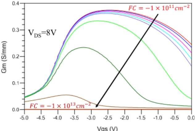
impact of FC at ①). Fig. 11 reports on the intrinsic transconductance gain gm variation for different FC
densities as depicted in #A, under the gate finger. Only the threshold voltage Vth shifts when FC density varies
in this case. When considering FC in the ungated zones of the HEMT (i.e. G-S or G-D zones), then IDSS (and
RON) changes as reported on gm profiles versus VGS in
Fig. 12, whereas Vth remains constant. T-CAD
simulations enable the FC effects at the interfaces of the #A gated zone to be differentiated from that in the
#B ungated zones over the electrical behaviours before and after application of the stress.
The average 35% reduction on IDSS is then
achieved by simulation using a higher FC density in the ungated zone #B (increase by FC=-1,2.1012 cm-2).
The sensitivity of Vth with fixed charge variationFC)
is constant whatever the initial FC density, and equal to Vth/FC= 0.5.10-12 V/cm-2. Then, simulations
corroborate well with the measurements (featuring +0.2V to +0.5V increase in Vth after HTOL stress, i.e.
6% to 15% in Fig. 1), if using a fixed charge density variation FC between 0,4.1012 cm-2 and 1012 cm-2. It is
also noticed a positive shift of Vth when performing
transient measurements as evidenced in [7]. Different evolutions can be found for Vth in the literature: a drift
towards more negative threshold values after stress periods is reported in [8], caused by substitutional and interstitial oxygen complexes but featuring recoverable effects due to the nature of these defects.
Two simulation plans are used as depicted in Fig. 10 ( #A and #B); an average of FC=1012 cm-2
variation in the density of fixed charge at the AlGaN/2DEG interface accounts both for the Vth shift
and for the IDSS reduction (first order G-S spacing and
second order G-D spacing). Fixed Charges variation between gate and drain account for the RON increase.
These results are consistent with some other papers, even if related to recoverable effects [10].
VDS=8V
Fig. 11. Simulated transconductance gain with VDS=8V for
different fixed charges densities FC under the gate finger (case #A, negative FC at interface ③). FC ranges from -0,25.1011 cm-2 to -1.1011 cm-2 (step 0,25.1011 cm-2), from
-0,25.1012 cm-2 to -1.1012cm-2 (step 0,25.1012 cm-2) and from
-0,25.1013 cm-2 to -1.1013cm-2 (step 0,25.1013 cm-2).
#A: under the gate finger #B: between G-S (or G-D) Fig. 10. HEMT cut view pattern for Fixed Charges (FC) density impact evaluation on electrical behaviors before and after stress application.
VDS=8V
Fig. 12. Simulated transconductance gain with VDS=8V for
different fixed charges densities FC under the ungate G-S (G-D) zone(s) (case #B, negative FC at interface ③). FC ranges from -0,25.1011 cm-2 to -1.1011 cm-2 (step 0,25.1011 cm-2),
from -0,25.1012 cm-2 to -1.1012cm-2 (step 0,25.1012 cm-2) and
4. Imaging with STEM HAADF and TEM lamella TEM analysis gives a direct proof of structural defects in GaN structures, and has led to major issues for GaN technology improvements from different works, as in [9]. Next studies on STEM HAADF and TEM lamella have been driven by DGA MI (French MoD) on HTOL stressed devices.
4.1. Scanning Transmission Electron Microscopy High Angle Annular Dark Field (STEM-HAADF) – section view
STEM-HAADF images are suitable to define clearly the interface between GaN, AlGaN, SiN passivation layer or Gate Schottky metal; a FIB cut in the gate region allows an imaging of the stacked layers. Strong contrast can be identified between the layers as proposed in Fig. 13 a and b (respectively in the gate-passivation zone and under the gate metal). Contrasted domains are noticed at the interface between the passivation layer and the AlGaN layer. This ‘unexpected’ layer is constituted with Ga, Al and O species (by EDX and EFTEM), and is considered to be resistive. This observation is consistent with the highly resistive behavior at low IGS (Fig. 8 and Fig. 9 inset).
4.2. TEM lamella by removing the gate metallization - top view
TEM lamella of the gate foot (top view after removing the metallization of the gate finger) is reported in Fig. 14; the presence of voids under the gate finger is consistent with the inhomogeneity of the SBH revealed in Fig. 6 and Fig. 7.
5. Conclusions
The identification of the impacting physical mechanism on the degradation of a (batch of) device(s) during the application of a stress is difficult to achieve. Usually, different contributors have to be considered together, but are not easily identifiable using a single method (experimental or simulation). Crossing dedicated measurements techniques and models with T-CAD simulations enlarges the field of investigation for failure analysis and process improvement. A failure analysis study case focused on gate Schottky diode inhomogeneity and interface states in the gated and ungated zones of the transistor have been presented.
It has been demonstrated the difficulty to achieve accurate Schottky Barrier Height extraction; the new proposed method accounts for the ideal SBH (extracted at 1.1eV), and also evidence different scattering processes on the SBH before and after the application of the HTOL stress.
From an electrical model developed at different temperatures, several gate current contributors have been extracted (evidencing two SBH paths); a focus was given on a highly resistive behavior occurring near the Thermionic Emission mode.
These results on the SBH inhomogeneity and on the highly resistive layer at the passivation/AlGaN interface corroborate with the different TEM analysis of the gate proposed in section view and top view.
T-CAD model has also been developed to assess the HTOL stress induced variations on IDSS and on Vth.
Fig. 14. TEM lamella of the gate finger (top view) performed by SERMA: identification of defects (voids) under the gate.
a) gate-source zone b) under the gate zone Fig. 13. STEM-HAADF images (FIB cut) performed by Biophy Research a) on the gate edge between gate and source and b) under the gate.
Fixed charge density variations at the AlGaN/2DEG interface have been used in the gated zone and in the ungated zones of the modeled transistor to account respectively for the Vth drift and for the IDSS reduction.
Results also corroborate well with measurement considering the impact of FC=1012 cm-2 on V
th and on
IDSS after combining the effects from each zone.
References
[1] J. H. Werner, H. H. Güttler, “Barrier inhomogeneities at Schottky contacts,” J. Appl. Phys., vol. 69, no. 3, pp. 1522–1533, 1991.
[2] R. T. Tung, “Electron transport at metal-semiconductor interfaces: General theory,” Phys. Rev. B, vol. 45, no. 23, pp. 13509–13523, 1992.
[3] S. Chand and J. Kumar, “Evidence for the double distribution of barrier heights in Pd2Si/n-Si Schottky diodes from I-V-T measurements,” Semicond. Sci. Technol., vol. 11, no. 8, pp. 1203–1208, 1996. [4] S. Karboyan et al. “Analysis of barrier inhomogeneities
in AlGaN/GaN HEMTs’ Schottky diodes by IVT measurements,” Eur. Microw. Integr. Circuits Conf. EuMIC, pp. 240–243, 2013.
[5] O. Lazăr et al.“New Approach for an Accurate Schottky Barrier Height’s Extraction by IVT Measurements,” IEEE Int. Microw. Symp. IMS, pp. 309–312, 2015. [6] R. Stevenson, “Understanding Imperfections in GaN
HEMTs” presented at CS Mantech, 2014. [7] D. Bisi et al.“Deep-level characterization in GaN
HEMTs – Part I : Adv. and limitations of Drain current transient measurements”, IEEE Trans. On Electron Devices, Vol. 60, No. 10, Oct. 2013, pp.3166-3175. [8] D.M. Fleetwood et al.“Oxygen-related border traps in
MOS and GaN devices” IEEE 11th Int. Conf. on
Solid-State and Integr. Circuit Techn. (ICSICT), 2012, 7p. [9] S.Y. Park, "Physical degradation of GaN HEMT
devices under high drain bias reliability testing", Microelectronics Reliability 49 (2009) 478–483. [10] M. Meneghini et al. "Negative Bias-Induced
Threshold Voltage Instability in GaN-on-Si Power HEMTs", IEEE EDL, Vol. 37, Issue 4 (2016) 474–477.
![Fig. 2. Representation of the parameters from Werner’s method applied to Richardson's model as expressed in [5]:](https://thumb-eu.123doks.com/thumbv2/123doknet/14401018.510012/3.892.470.766.581.1015/representation-parameters-werner-method-applied-richardson-model-expressed.webp)