HAL Id: hal-01204711
https://hal.archives-ouvertes.fr/hal-01204711
Submitted on 3 Apr 2017HAL is a multi-disciplinary open access
archive for the deposit and dissemination of sci-entific research documents, whether they are pub-lished or not. The documents may come from teaching and research institutions in France or abroad, or from public or private research centers.
L’archive ouverte pluridisciplinaire HAL, est destinée au dépôt et à la diffusion de documents scientifiques de niveau recherche, publiés ou non, émanant des établissements d’enseignement et de recherche français ou étrangers, des laboratoires publics ou privés.
Growth and characterization of gallium oxide thin films
by radiofrequency magnetron sputtering
Philippe Marie, Xavier Portier, Julien Cardin
To cite this version:
Philippe Marie, Xavier Portier, Julien Cardin. Growth and characterization of gallium oxide thin films by radiofrequency magnetron sputtering. physica status solidi (a), Wiley, 2008, 205 (8), pp.1943-1946. �10.1002/pssa.200778856�. �hal-01204711�
Growth and characterization
of gallium oxide thin films
by radiofrequency magnetron sputtering
P. Marie*
, X. Portier, and J. Cardin
CIMAP-CEA-CNRS-ENSICAEN-Université de Caen, 6 Boulevard Maréchal Juin, 14050 CAEN Cedex 4, France
* Corresponding author: e-mail philippe.marie@ensicaen.fr
1 Introduction Recently, transparent conductive ox-ide (TCO) as alternative to expensive ITO have focused much attention owing to the wide variety of possible appli-cations such as optical windows [1, 2], high temperature chemical gas sensor [3], and dielectric layer [4]. Gallium zinc oxide (GZO) thin films have shown high conductivity and transparent properties with figure of merit comparable to those of ITO materials [5]. Among promising TCO ma-terials, Ga2O3 is a wide band gap semiconductor material (4.9 eV) and its conductivity can vary from insulator to conductor depending on the growth conditions [1, 2]. Over the past few years, by doping this material with rare-earth elements or 3d transition metal ions, Ga2O3 thin films have also shown promising optical and photoluminescent (PL) properties [6] as well as possible applications in electrolu-minescent devices (thin film electroluelectrolu-minescent displays) [7]. The most suitable structure for applications is the monoclinic β-Ga2O3 phase (a = 1.221 nm, b = 0.304 nm,
c = 0.580 nm and β = 103.8°, space group: C2/m) which appears to be extremely stable chemically and thermally (melting point at 1800 °C) and may be an alternative choice to other transparent conductive oxide (TCO) mate-rials (sulphide-based phosphors) usually dedicated to opto-electronic devices. Various growth techniques have been
used to prepare thin films of this material: electron beam evaporation [8], spray pyrolysis deposition [9], sol gel process [7] and radiofrequency (RF) magnetron sputtering [10].
In the present paper, we report the use of RF magne-tron sputtering to prepare undoped β-Ga2O3 thin films. Structural characterizations, optical absorption as well as electrical conductivity properties are studied versus anneal treatments during and after the growth process. In addition, Nd-doped β-Ga2O3 thin films have been fabricated by co-sputtering and the first PL data show the emitting signa-tures of the rare earth element in the infrared spectral region.
2 Experimental details Gallium oxide Ga2O3 thin
films were prepared by radio-frequency magnetron sputter-ing of a Ga2O3 (99.99% purity) target. Before any deposit,
the chamber was evacuated down to 1.0 × 10⁻⁷ Torr. The substrate temperature (Ts) during deposit was varied over
the range 100 – 600 °C. Then the layers were grown on sin-gle crystal silicon substrates under a pure argon pressure of 2.5 × 10⁻² Torr and a power density of 2.5 W/cm2. The thickness of the deposited films ranged between 250 nm and 600 nm. For each Ts value, (100)-oriented silicon sub-Undoped and Neodymium-doped gallium oxide (Ga2O3) thin
films of about 500 nm thickness were successfully grown at different temperatures ranging from 100 up to 600 °C by radiofrequency magnetron sputtering. Post-annealing treat-ments were carried out at 900 °C and 1000 °C. The obtained films were (400) textured and a grain size of a few tens of
nanometres was found. Optical and electrical characteriza-tions led to a figure of merit of about 1.9 × 10⁻⁴. These films were successfully doped with Neodymium by a co-sputter-ing method. The photoluminescence experiments for the Nd-doped β-Ga2O3 films clearly showed the rare-earth emit-ting signature.
strates were placed in the chamber, side by side and at 7 cm just above the target. Post-annealing treatments were carried out at Ta = 900 °C and 1000 °C during 1 hour under a continuous flow of pure nitrogen. Nd-doping was achieved by placing a few pellets of Neodymium oxide on the target surface during the growth process corresponding to a surface ratio of about 5%.
Various characterization techniques were used to ana-lyse the evolution of the structural, optical and electrical properties of the films upon growth conditions (Ts) and post-anneal treatments (Ta). X-ray spectroscopy measure-ments were performed using a Philips XPERT diffractom- eter with Cu Kα (λ = 1.5418 Å) as X-ray source. Usual θ–2θ diagrams were recorded under a grazing incidence of 0.5°. Conventional and high resolution Transmission Elec-tron Microscopy (TEM) observations of cross sectional views of the films were performed using a JEOL 2010F operated with a Field Emission Gun source at 200 kV, and equipped with a CCD camera. The ellipsometric spectros-copy (ES) data were collected while the incident light was scanned between 1.5 eV and 5.0 eV under an incidence angle of 66.2°. This was realized by means of a Jobin – Yvon ellipsometer (UVISEL). The ES spectra consist in the measurement of ψ and ∆ ellipsometric angles defined from the fundamental equation of ellipsometry:
p s tan ei
r r = ψ ∆
, (1)
where rp and rs are the complex reflection coefficients for parallel and perpendicular polarizations of the light, re-spectively. The sheet resistance is a measure of resistance of thin films that have a uniform thickness. It is applicable to two-dimensional systems where the thin film is consid-ered to be a two dimensional entity and is equivalent to re-sistivity as used in three-dimensional systems. In a regular three-dimensional conductor, the resistance can be written as: , L R eW ρ = (2)
where ρ is the resistivity, L is the length, W is the width and e the sheet thickness. By grouping the resistivity with the thickness, the resistance can then be written as:
s L
R R W
= with Rs = ρe . (3)
Rs is then the sheet resistance in ohms/square (W/䊐).
For a square, L = W and therefore, R = Rs. PL response was investigated at room temperature using an Ar laser line which induces a resonant excitation of Nd (operating at 514 nm). The emission was recorded through a system of measurement composed by a chopper, a monochromator (Jobin – Yvon THR1000) followed by a cooled Ge detector and a lock-in amplifier. The PL measurement was carried out with a laser beam chopped at 45 Hz and an excitation power of 1.3 W/cm2.
3 Results and discussion
3.1 Substrate temperature effect All the
synthe-sised films were found to be amorphous whatever the cho-sen Ts value. The XRD patterns obtained for all the Ts val-ues (not shown) give rise to similar spectra: two broad bands centred at about 32° and 64° are visible. These posi-tions correspond approximately to the posiposi-tions of the main diffraction peaks of β-Ga2O3. These broad bands could suggest the presence of a nanocrystalline structure of the films but TEM observations (not shown) showed that they were fully amorphous. The films were also subject to SE analyses by using a model dealing with an appropriate dispersion law such as Forouhi – Bloomer [11] and the Bruggeman effective medium approximation (EMA) [12]. Such analyses were already described elsewhere in the case of silicon nanoparticles embedded in a silica matrix [13].
The deduction of the optical parameters from the ellip-sometric angles ψ and ∆ requires the reproduction of the experimental values in the energy range 1.5 – 5 eV. Al-though the EMA approach could appear more realistic for our material that might be considered as containing com-ponents of both crystalline and amorphous Ga2O3, it re-quires, however, the existence of reference spectra for these media. As example, we chose as a reference for sili-con substrate, data sili-contained in the software DELTAPSI2 from Jobin – Yvon. Concerning the Ga2O3 films, the
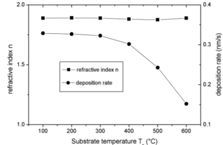
disper-sion law which models the dielectric function, called “new amorphous” has been used. It derives from the Forouhi – Bloomer law, commonly used in the case of both semicon-ducting and insulating materials. A nearly perfect agree-ment between the measured and calculated spectra was ob-tained and the thickness agrees well with that obob-tained by other techniques. However, the major data extracted from the modelling are the optical properties as will be dis-cussed hereafter. Figure 1 depicts the static (in the infrared region) refractive index spectra n and the deposition rate as
Figure 1 Static refractive index (n) and deposition rate versus
substrate temperature. n is constant with a value (about 1.91) close to that of bulk Ga2O3and the deposition rate is decreasing when Ts is raised.
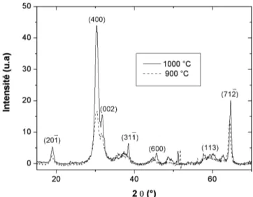
Figure 2 X-ray diffraction patterns of annealed gallium oxide
films. Diffraction peaks positions are consistent with the mono-clinic β-Ga2O3 structure. The high intensity of the (400) peak suggests a (400) texture of the film.
a function of the substrate temperature Ts. Upon increasing Ts, n is almost constant (close to the value of bulk Ga2O3,
n = 1.91) whereas the deposition rate decreases in a monotonous way. This behaviour is usual and is explained by a larger reactivity of the species produced within the plasma when Ts increases [14].
3.2 Annealing temperature effect Anneal
treat-ments were performed on films grown at Ts = 100 °C.
Fig-ure 2 shows the XRD spectra of gallium oxide thin films annealed at 900 °C and 1000 °C under a continuous flow of pure nitrogen. Diffraction peaks appear for both samples and their positions are consistent with the monoclinic structure of Ga2O3 (β-Ga2O3). However, higher intensities are observed for the sample annealed at 1000 °C indicating a better formation of the β-Ga2O3 phase.
Compared to a diffraction spectrum of a powder β-Ga2O3 specimen, the intense (111) diffraction peak is miss-ing and the highest intensity is observed for the peak related to the (400) planes suggesting thus a (400) preferred orienta-tion of the films. There is no observable secondary phase in the XRD patterns. TEM observations led to an estimate of the grain size of a few tens of nanometres. Figure 3(a) is a typical HREM image of a film annealed at 1000 °C. This re-gion shows a grain oriented such that the Fourier transform in Fig. 3(b) is in accordance with the monoclinic structure of Ga2O3. The grain orientation is also consistent with the above mentioned (400) texture of the films.
Figure 3 (a) HREM image of an annealed film at 1000 °C, (b)
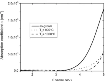
Fourier transform of the image in Fig. 3(a). These data confirm the formation of β-Ga2O3 and the (400) texture of the films. The Ta effect on the absorption coefficient α is shown in Fig. 4 which compares the α(E) spectra obtained from ellipsometry measurements for as-grown and annealed samples. These data reveal that all the samples are almost transparent below 3 eV whereas a clear improvement ap-pears when Ta increases.
However, close to 5 eV, the Ta effect is weak. This be-haviour shows that the thin films become more transparent after post-annealing than for the as-grown sample. Anneal-ing treatment allows certainly a crystallization of the films whose composition becomes close to that of the target. This seems to be confirmed by the electrical measurements. Indeed, Table 1 gives the values of the sheet resistances obtained for as-grown and annealed samples. One observes a decrease in resistance with Ta and thus indicates an im-provement of the film conductivity. In Table 1 are also re-ported the absorption coefficient values at E = 2.3 eV (cor-responding to the medium of the visible range) and the transmission coefficients of the films calculated by
e x
T = -α . It is then possible to calculate the figure of merit
TC
Φ of the transparent conductive sample by the following equation: 10 TC s . T R Φ = (4)
The obtained values show that they are very satisfac-tory compared to those of other operating TCOs (about 1.0 × 10⁻³ for ZnO [15], and 2.0 × 10⁻³ for ZGO [16] and we can observe an increase of this factor with the anneal-ing temperature.
Regarding the Nd-doped β-Ga2O3 films, optical
proper-ties are very close to those of non doped films. By EDX analysis, the Nd concentration does not exceed 1% corre-sponding to the detection limit of the spectrometer. Fig-
Table 1 Electrical and optical data of the gallium oxide films.
sample L (mm) e (nm) W (mm) R (Ω) Rs (Ω/) α (cm–1) T Φ (Ω–1) as-grown 10 544 5 3947 7895 431.0 0.98 1.0 × 10⁻⁴ 900 °C 10 590 5 3409 6818 7.4 1.00 1.5 × 10⁻⁴ 1000 °C 6 590 5 2113 2535 1370 0.93 1.9 × 10⁻⁴
Figure 4 Dependence of the absorption coefficient on anneal
temperature. The grown material is transparent in the visible range (from 1.6 up to 3.2 eV).
ure 5 exhibits the PL response of the Nd-doped β-Ga2O3 film annealed at 1000 °C.
The rare-earth signature is clearly visible at 880 nm and 1070 nm corresponding respectively to 4F transitions respectively 4F3/2→ 4I11/2 and 4F3/2→ 4I9/2 of Nd3+. This first result is encouraging and optimisation of the process is in progress. For instance, the effect of the number of pel-lets on the target as well as the anneal treatment has to be investigated and optimised. Very recently, a similar ap-proach using a subdivided powder target into two or more parts led to multicomponent thin film phosphors for elec-troluminescent devices [17]. Our goal is to obtain similar results with our method.
Figure 5 PL spectrum for the Nd-doped β-Ga2O3 film annealed at 1000 °C. Nd signature is clearly identified by the presence of two peaks of luminescence at 880 nm (a) and 1070 nm (b).
4 Conclusion β-Ga2O3 polycrystalline thin films have
been successfully grown by RF magnetron sputtering. The β-Ga2O3 phase appears upon an anneal treatment at about
900 °C. The grain size is a few tens of nanometres and the films are (400) textured. A Ta increase favours a better figure of merit up to 1.9 × 10⁻⁴ for Ta = 1000 °C. A possi-ble application of this material is transparent electrodes under extreme thermal conditions. Nd-doped films have been achieved with success since the typical emitting sig-nals from Nd in the infrared region have been easily de-tected. This co-sputtering method of doping β-Ga2O3 films is then promising and will be optimised to fabricate light emitting diodes. These studies will be extended to other rare-earth elements.
References
[1] M. Passlack, E. F. Schubert, W. S. Hobson, M. Hong, N. Moriya, S. N. G. Chu, K. Konstadinis, J. P. Mannaerts, M. L. Schnoes, and G. J. Zidzik, J. Appl. Phys. 77, 686 (1995).
[2] T. Minami, Semicond. Sci. Technol. 20, 35 (2005).
[3] M. Fleisher and H. Meixner, Sens. Actuators B 4, 437 (1991).
[4] M. Passlack, N. E. J. Hunt, E. F. Schubert, G. J. Zidzik, M. Mong, J. P. Mannaerts, R. L. Opila, and R. J. Fischer, Appl. Phys. Lett. 64, 2715 (1994).
[5] E. Fortunato, V. Assunçao, A. Gonçalves, A. Marques, H. Aguas, L. Pereira, I. Ferreira, P. Vilarinho, and R. Mar-tins, Thin Solid Films 451, 443 (2004).
[6] A. Shionoya and W. M. Yen, Phosphor Handbook (CRC Press, Boca Raton, FL, 1998).
[7] T. Miyata, T. Nakatani, and T. Minami, J. Lumin. 87–89, 1183 (2000).
[8] A. Callegari, P. D. Hoh, D. A. Duchanan, and D. Lacey, Appl. Phys. Lett. 54, 332 (1989).
[9] J. Hao and M. Cocivera, J. Phys. D, Appl. Phys. 35, 433 (2002).
[10] T. Minami, H. Yamada, Y. Kubota, T. Myata, and Y. Saka-gami, Proc. of the Fourth International Display Workshop, 1997, p. 605.
[11] A. R. Forouhi and I. Bloomer, Phys. Rev. B 34, 7018 (1989). [12] D. A. G. Bruggeman, Ann. Phys. 24, 636 (1935).
[13] S. Charvet, R. Madelon, F. Gourbilleau, and R. Rizk, J. Appl. Phys. 85, 257 (1999).
[14] H. Colder, R. Rizk, M. Morales, P. Marie, and J. Vicens, J. Appl. Phys. 98, 24313 (2005).
[15] L. Raneiro, A. Gonçalves, A. Pimentel, I. Fer- reira, S. Zhang, L. Pereira, H. Aguas, E. Fortunato, and R. Martins, Mater. Res. Soc. Symp. Proc. 862, A21.10.1 (2005).
[16] L. Raniero, I. Ferreira, A. Pimentel, A. Gonçalves, P. Can-hola, E. Fortunato, and R. Martins, Thin Solid Films 511, 295 (2005).
[17] T. Minami, Y. Mochizuki, and T. Miyata, Thin Solid Films 494, 33 (2006).
View publication stats View publication stats