HAL Id: hal-02461174
https://hal.archives-ouvertes.fr/hal-02461174
Submitted on 7 Jan 2021
HAL is a multi-disciplinary open access
archive for the deposit and dissemination of
sci-entific research documents, whether they are
pub-lished or not. The documents may come from
teaching and research institutions in France or
abroad, or from public or private research centers.
L’archive ouverte pluridisciplinaire HAL, est
destinée au dépôt et à la diffusion de documents
scientifiques de niveau recherche, publiés ou non,
émanant des établissements d’enseignement et de
recherche français ou étrangers, des laboratoires
publics ou privés.
Pierre Demongodin, Houssein El Dirani, Jérémy Lhuillier, Romain
Crochemore, Malik Kemiche, Thomas Wood, Ségolène Callard, Pedro
Rojo-Romeo, Corrado Sciancalepore, Christian Grillet, et al.
To cite this version:
Pierre Demongodin, Houssein El Dirani, Jérémy Lhuillier, Romain Crochemore, Malik Kemiche, et
al.. Ultrafast saturable absorption dynamics in hybrid graphene/Si 3 N 4 waveguides. APL Photonics,
AIP Publishing LLC, 2019, 4 (7), pp.076102. �10.1063/1.5094523�. �hal-02461174�
hybrid graphene/Si
3
N
4
waveguides
Cite as: APL Photonics 4, 076102 (2019); https://doi.org/10.1063/1.5094523Submitted: 03 March 2019 . Accepted: 17 June 2019 . Published Online: 18 July 2019
Pierre Demongodin, Houssein El Dirani, Jérémy Lhuillier, Romain Crochemore, Malik Kemiche, Thomas Wood, Ségolène Callard, Pedro Rojo-Romeo, Corrado Sciancalepore, Christian Grillet, and Christelle Monat
COLLECTIONS
This paper was selected as Featured
ARTICLES YOU MAY BE INTERESTED IN
Brillouin optomechanics in nanophotonic structures
APL Photonics
4, 071101 (2019);
https://doi.org/10.1063/1.5088169
Nonlinear optics in carbon nanotube, graphene, and related 2D materials
APL Photonics
4, 034301 (2019);
https://doi.org/10.1063/1.5051796
Strong frequency conversion in heterogeneously integrated GaAs resonators
Ultrafast saturable absorption dynamics in hybrid
graphene/Si
3
N
4
waveguides
Cite as: APL Photon. 4, 076102 (2019);doi: 10.1063/1.5094523 Submitted: 3 March 2019 • Accepted: 17 June 2019 •
Published Online: 18 July 2019
Pierre Demongodin,1,a) Houssein El Dirani,2 Jérémy Lhuillier,1 Romain Crochemore,2 Malik Kemiche,1
Thomas Wood,1 Ségolène Callard,1 Pedro Rojo-Romeo,1 Corrado Sciancalepore,2 Christian Grillet,1
and Christelle Monat1
AFFILIATIONS
1Université de Lyon, Institut des Nanotechnologies de Lyon (INL) UMR 5270, École Centrale de Lyon, 69134 Écully, France 2Université Grenoble Alpes, CEA-LETI, Minatec, Optics and Photonics Division, 17 rue des Martyrs, F-38054 Grenoble, France a)Electronic mail:pierre.demongodin@ec-lyon.fr
ABSTRACT
We study the nonlinear optical properties of graphene integrated onto Si3N4waveguides under picosecond and subpicosecond pulsed
exci-tation at telecom wavelength. Saturable absorption of graphene under guided-mode exciexci-tation is measured, and the temporal effects related to the photoexcited carrier dynamics in graphene are highlighted. Thereafter, a model of photoexcited carriers in graphene is implemented into the nonlinear Schrödinger equation in order to simulate the pulse propagation across the hybrid graphene/Si3N4waveguide. This allows
us to extract phenomenological parameters of graphene saturable absorption in chip-based devices, which could provide some guidelines for the design of nonlinear elements in photonic integrated circuits.
© 2019 Author(s). All article content, except where otherwise noted, is licensed under a Creative Commons Attribution (CC BY) license (http://creativecommons.org/licenses/by/4.0/).https://doi.org/10.1063/1.5094523., s
I. INTRODUCTION
Over the past decade, graphene, a bi-dimensional lattice of carbon atoms, has generated plenty of interest for both funda-mental and applied research in microelectronics and more recently in optoelectronics.1,2Its unique properties,3 mostly related to the Dirac cone electronic dispersion,4 make it an outstanding mate-rial candidate for both electronic and photonic device applica-tions.5–8Among all relevant properties, the optical nonlinearity of graphene was pointed out to be much larger than those in traditional semiconductor and glass materials.9–11 In addition, this nonlinear response could be dynamically tuned through electrical gating,12–15 with the prospect of realizing fast, reconfigurable, and flexible non-linear devices. Last but not least, the planar geometry of graphene makes it relatively easy to transfer this carbon layer onto photonic chips, as part of postprocessing techniques. Integrated optics can indeed bring what graphene lacks due to its atomic layer thick-ness, i.e., a way to reinforce the interaction between light and this 2D-material through the use of resonant or light-confining geome-tries. Graphene could thus lead to a new generation of nonlinear photonic devices and chips that combine the existing know-how
on integrated optics with graphene strong and tunable nonlinear properties.
On the one hand, several χ(3) based nonlinear effects in graphene have been investigated theoretically9,10,16,17 and experi-mentally. Related measurements using either free-space excitation or interaction with guided light waves have demonstrated four-wave mixing,11,13,18–20 self-phase modulation,21–23 and third har-monic generation.24,25 However, all these works have reported a large disparity in the quantitative estimation of the third-order non-linear refractive optical response.14,16This issue remains still poorly understood and could be attributed to the different experimental conditions used to probe graphene, to the quality of graphene itself, or to the material environment in the vicinity of graphene. In par-ticular, the unambiguous extraction of the nonlinear response of graphene is not straightforward when this 2D material is deposited on top of another nonlinear refractive material, like silicon, for instance.
On the other hand, graphene is known to act as a saturable absorber.26–28 This nonlinear signature has been widely used for the realization of passively mode-locked fiber lasers.29–34Although
some theoretical papers attempted to model saturable absorption in graphene,26,27 the correlation with experimental studies is still imperfect.27More importantly, its implementation onto chip-based platforms remains elusive but could form the critical nonlinear ele-ment of either integrated mode-locked lasers or more generally advanced photonic integrated circuits, such as chip-based photonic neural networks and programmable nanophotonic processors.35So far, most studies have focused on either third-order nonlinear refrac-tive processes or saturable absorption separately. However, these two effects are likely to occur under a similar regime of excitation, and their interplay cannot be ignored. Although not directly investigat-ing the effect of saturable absorption, Vermeulenet al.21 recently pointed out that self-phase modulation in glass waveguides covered with graphene could be explained by the generation of free carri-ers in graphene and the related change in refractive index at the time scale of the picosecond pulse duration used in the experiment. This suggests that saturable absorption of graphene could have a non-negligible impact on third-order nonlinear refractive processes. Most importantly, the time scale of free carrier recombination in graphene, which is known to be much shorter (∼1 ps) than in tradi-tional semiconductor materials, might have important consequences on the dynamics and magnitude of these nonlinear effects. In Ref.21, saturable absorption was not reported, possibly due to the low power regime (∼2 W peak power) that was used. In addition, the effects of carrier dynamics, as dictated by the temporal pulse duration of the pump, were not fully investigated.
In this work, we demonstrate the signature of saturable absorp-tion of graphene in chip-based platforms by measuring the trans-mission of near-infrared optical pulses in hybrid graphene/Si3N4
waveguides. We take advantage of the relatively weak nonlinear properties of the underlying Si3N4 material for studying
unam-biguously graphene nonlinear properties. From our measurements across a large dynamic range of pulse peak power (from 0.2 W up to a few hundreds), we observe a substantial rise of the transmission by more than a factor 2, which increases with graphene interaction length. By varying the pulse duration from the picosecond to sub-picosecond, we also report a variation of the absorption saturation of graphene, thereby revealing some dynamics of this effect. We correlate these measurements with a nonlinear pulse propagation model taking into account graphene interaction length, the linear
and nonlinear response of the hybrid waveguide, power-dependent loss in graphene, and the associated dynamics of free carrier relax-ation. These studies attempt to clarify the interplay between sat-urable absorption and third-order nonlinear refractive processes in graphene, which should help realize more efficient graphene based nonlinear devices on a chip.
II. GRAPHENE ON SILICON NITRIDE HYBRID DEVICES AND LINEAR MEASUREMENTS
The photonic chip used for the characterization of graphene nonlinear optical properties features 2 cm long Si3N4waveguides
buried in silica.36,37 The silica top cladding of the waveguides was removed using a perfectly selective chemical-mechanical pla-narization, so as to leave the waveguides top surface exposed in air with no Si3N4 consumption and no remaining
topogra-phy. The cross section dimensions of the Si3N4 waveguides are
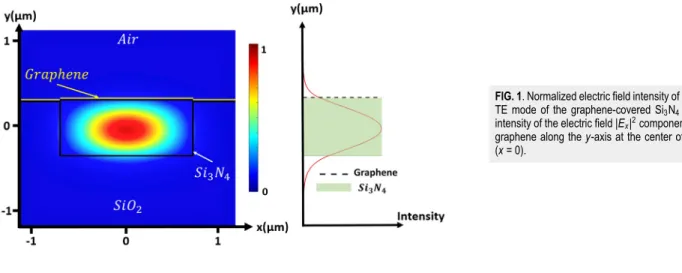
1.5 μm × 0.66 μm (width × height). Figure 1 displays the elec-tric field intensity of the fundamental TE mode that will be excited in our experiments. Butt-coupling transmission measure-ments of a series of these unclad Si3N4 waveguides with
differ-ent lengths allowed us to extract waveguide propagation losses of 3 dB/cm and coupling loss of around 4 dB per facet. The latter is lowered, thanks to the use of inverse tapers close to the chip input/output.
Trivial transfer graphene, purchased from ACS Materials
®
, was transferred onto the chip. The waveguide planarization step men-tioned above allows us to take advantage of an increased interaction between the guided mode and graphene that lies directly on the surface of the waveguide. We also note that this geometry conve-niently presents a planar surface that is ideal for the mechanical transfer of graphene. As shown in the optical microscope image of Fig. 2(a), the transfer provides us with a series of waveguides with a variable coverage of graphene. Four waveguides are available for study, with a graphene interaction length of 0.5, 1.4, 2.3, and 3.2 mm. An additional Si3N4waveguide without graphene will be used as areference.
Raman measurements were performed after the transfer, and a typical spectrum obtained in the vicinity of the waveguides of interest is shown inFig. 2(b). The characteristics of this spectrum
FIG. 1. Normalized electric field intensity of the fundamental
TE mode of the graphene-covered Si3N4waveguide and
intensity of the electric field |Ex|2component in the plane of
graphene along the y-axis at the center of the waveguide (x = 0).
FIG. 2. (a) Optical microscope image of the graphene
trans-ferred onto Si3N4optical waveguides. (b) Raman spectrum
of the graphene covered chip. The AG/A2Dratio suggests
that graphene has a monolayer thickness while the absence of D peak confirms the quality of graphene.
(the integrated intensity ratio of the G and 2D band, AG/A2D, in
particular) confirm the presence of monolayer graphene.38
Using a low power continuous-wave laser at 1540 nm coupled to the chip (with ∼30 μW power) in the TE-polarization, we charac-terize the linear response of the hybrid graphene/Si3N4waveguides.
Figure 3(a)shows the total transmission of the waveguides as a func-tion of the length of graphene that covers them. The coupling loss per facet is relatively unchanged with respect to that of the unclad Si3N4waveguides, and the slope of the linear (dB scale)
transmis-sion allows us to infer an average propagation loss α0of 126 dB/cm
induced by the presence of graphene. The good linear fit (R2= 0.991) of the transmission with graphene length seems to confirm the rel-atively homogeneous properties (at least at the millimeter scale) of graphene transferred onto the chip. In addition, the high optical losses of the graphene-covered waveguides attest the strong inter-action between the mode and graphene. This loss figure is consistent with the overlap of graphene with the evanescent tail of the waveg-uide TE fundamental mode (around 0.013% of the intensity field, considering an effective thickness of 3.3 Å for graphene). The com-parison of linear modal loss measurements of our hybrid waveguides across the wavelength range 1440 nm–1640 nm with simulations (Lumerical commercial software) allows us to extract a Fermi level of around −0.3 eV corresponding to an approximate p-doping of 9 × 1012cm−2, which is expected for CVD graphene and this trans-fer process.39 InFig. 3(b), we plot the effective length calculated
through40Leff = 1−exp
−α0Lgr
α0 as a function of the physical graphene interaction lengthLgr varying between 0.5 mm and 3.5 mm. This
curve gives an estimate of the waveguide length along which light effectively propagates before it gets fully absorbed. This effective length saturates beyond 1.5 mm graphene length due to the high linear propagation losses of the hybrid waveguide. This suggests that we might not observe much difference in terms of the related nonlin-ear signature when probing waveguides covered by graphene length beyond 1.5 mm.
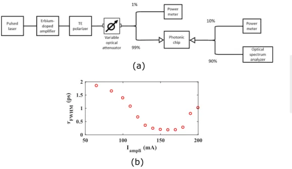
III. NONLINEAR CHARACTERIZATION SETUP
For the study of the nonlinear properties of the graphene-covered waveguides, we use a fiber-based pulsed laser that delivers ∼2 ps pulses at 1547 nm and with a repetition rate of 20 MHz. The setup is presented schematically inFig. 4(a): it includes a polarizer so as to excite the TE mode of the chip and a variable optical attenu-ator to vary the pump power coupled to the waveguides using lensed fibers. 1% of the input power is tapped for monitoring the pump power coupled to the chip, while a coupler at the output allows us to measure both the spectrum (via an optical spectrum analyzer) and the power collected at the end of the waveguides (via a power meter). To reach higher peak powers, we amplify the nearly Fourier-transform limited pulses from the laser using an Erbium Doped Fiber Amplifier (EDFA). The use of this EDFA gives us some
FIG. 3. (a) Measured waveguide transmission (circles) as a
function of the interaction length with graphene. The red line is a linear fit associated with a slope of 126 dB/cm. (b) Effec-tive length as a function of the graphene interaction length forα0 = 126 dB/cm. The circles highlight the graphene lengths that are available on the sample.
FIG. 4. (a) Fiber optic setup used for
the measurements of the graphene cov-ered Si3N4waveguides in the nonlinear
regime. (b) Relation between the input pulse duration (FWHM) at the entrance of the chip and the pump current of the amplifier, as measured with a commer-cial autocorrelator.
flexibility in terms of pulse duration, allowing us to investigate the dynamics of the graphene/Si3N4waveguide nonlinear response. For
EDFA pump currents above a certain threshold (typically 85 mA in our setup), the amplified pulses are modified in both the spectral and temporal domains at the entrance of the chip. In particular, the combined effects of nonlinearity along the fiber (basically self-phase modulation) and its negative dispersion at 1547 nm induce some temporal compression of the pulse, depending on the amplified pulse peak power.
Practically, as we increase the EDFA pump current, the initially Fourier-transform limited pulse narrows in the temporal domain (for pump current up to ∼160 mA) until a minimum temporal width is reached. For EDFA pump current above 160 mA, the pulse dura-tion increases due to a gradual splintering of the pulse in the time domain. Therefore, it is possible to adjust the pulse duration by changing the EDFA pump current, while independently controlling the pump peak power (i.e., the pulse energy) coupled to the chip via the attenuator. Autocorrelation measurements of the input pulses close to the entrance of the chip were performed so as to provide an estimation of the input pulse duration.Figure 4(b)shows the rela-tion between the inferred pulse durarela-tion and the EDFA pump cur-rent. Our autocorrelation measurements show variations of about one order of magnitude, from 2 ps (initial pulse duration at the output of the laser) down to 0.2 ps approximately. This additional degree of freedom via controlling the EDFA pump current allows us to investigate the dependence of the nonlinear effects on the pulse duration on the nonlinear effects occurring in the hybrid graphene/Si3N4waveguides.
IV. EXPERIMENTAL NONLINEAR RESULTS
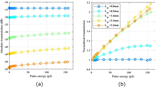
We first present the nonlinear transmission of graphene/Si3N4
waveguides when excited by subpicosecond pulses at 1547 nm with increasing peak power and a fixed pulse duration (∼0.2 ps, for an EDFA pump current of 160 mA). Figure 5shows the waveguide
transmission as a function of the coupled pulse energy, ranging between 0.15 and 150 pJ (i.e., 0.6–600 W coupled peak power), for the series of waveguides covered with different graphene lengths. Figure 5(a) exhibits the absolute transmission of the waveguides, whereasFig. 5(b)displays the normalized transmission, i.e., divided by the transmission at low energy (Epulse= 3 pJ) for each waveguide.
Figure 5(b)thus allows us to appreciate and compare the relative variation in transmission for the waveguides covered by different graphene lengths (between 0.5 mm and 3.2 mm), along with the reference waveguide (darkest blue) without graphene.
As a first observation, the transmission increases with pulse energy whenever graphene is present, while the reference curve (without graphene) remains flat, thereby confirming that the rise in transmission is related to graphene. Second, the rise in transmis-sion is somewhat correlated with the graphene interaction length, at least between 0 mm, 0.5 mm, and the three other lengths. We attribute these observations to the saturable absorption of graphene. We highlight that this signature is not hidden here by other kinds of nonlinear absorption loss that might otherwise occur at these power levels in the underlying waveguide such as, for instance, in silicon waveguides.
In the case ofLgr= 0.5 mm [lightest blue inFig. 5(b)], the
mea-sured increase in transmission rolls off above 100 pJ. We explain this clamping behavior by a nonsaturable absorption component of graphene, as the maximum transmission value (−20 dB) remains well below that of the waveguide without graphene (−14 dB) as observed inFig. 5(a).
For graphene lengths between 1.4 mm and 3.2 mm, the trans-mission continuously increases with pulse energy by more than a factor two with respect to the low power transmission. The simi-lar signature observed for the three longest graphene/Si3N4
waveg-uide is somewhat expected due to the saturation of the effective length (considering the hybrid waveguide propagation loss) beyond 1.5 mm of graphene length, which reaches a constant value of aroundLmaxeff = 0.345 mm. Qualitatively, once the effective length
FIG. 5. (a) Absolute transmission as a
function of the coupled pulse energy (Iampli = 160 mA, τFWHM = 0.2 ps,
20 MHz, 1547 nm) for Si3N4waveguides
covered by different graphene lengths. (b) Related normalized transmission for the same series of waveguides, where each transmission curve is normalized by the corresponding transmission at low pulse energy (Epulse= 3 pJ).
is reached (at ∼1.5 mm propagation distance), the pulse energy becomes too weak to induce any absorption saturation in the remaining section of graphene further in the waveguide. From our experimental results, we can thus conclude that graphene absorp-tion saturaabsorp-tion almost exclusively occurs in the first millimeter and half of our hybrid waveguides under the probed range of pulse energies.
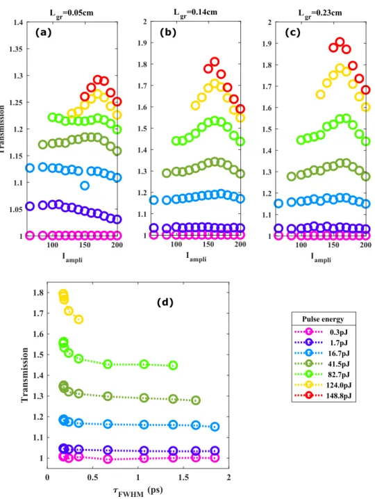
Next, we investigate the effect of pulse duration on the satu-ration of graphene absorption, by varying the pump current of the EDFA, while controlling the average power (i.e., the pulse energy) coupled to the waveguide using the variable optical attenuator. As already explained, the pump current of the EDFA affects the pulse shape and duration, i.e., the temporal distribution of pump pho-tons, while the attenuator sets the pulse energy, i.e., the number of photons comprised in the pulse. We can therefore control the pulse energy and duration relatively independently. However, the range of pulse duration that can be investigated for higher pulse energies is restricted by the high amplification gain requirements, as provided by the EDFA under higher pump currents. This leads to a narrower range of (short) pulse duration that can be probed for higher pulse energies.
In order to study how the pulse duration impacts saturable absorption of graphene, we measure the waveguide transmission while varying the EDFA pump current (i.e., pulse duration) for a fixed pulse energy. We thus only change how photons are tempo-rally distributed but not their number.Figure 6shows the results of these measurements. We plot the transmission (normalized with respect to the low pulse energy transmission at the lowest EDFA pump current setting) as a function of the EDFA pump current, with different colors used for different values of coupled pulse energy (between 0.3 pJ and 148.8 pJ). The results are shown for three hybrid graphene/Si3N4waveguides covered with 0.5 mm [Fig. 6(a)],
1.4 mm [Fig. 6(b)], and 2.3 mm [Fig. 6(c)] graphene lengths. To re-emphasize the link between the EDFA pump current and the pulse duration, we also present inFig. 6(d)the related normalized trans-mission vs the pulse duration inferred from these measurements for the caseLgr= 2.3 mm and EDFA pump current below 170 mA.
First, we notice a global increase in the transmission with the pulse energy at all EDFA pump currents, which corroborates the absorption saturation results fromFig. 5, independently of the pulse duration. Next, we see that for a fixed pulse energy (one colored curve inFig. 6), the normalized transmission increases with decreas-ing pulse duration, with a maximum obtained around 160 mA EDFA current corresponding to the shortest pulses. This behavior is more striking for higher pulse energies, while at low values of 0.3 pJ and 1.7 pJ, the increase in transmission is very weak due to the limited amount of saturable absorption.
These results suggest that temporal effects occur at the pulse time scale, while the pulse propagates through the hybrid graphene/Si3N4waveguide, related to the free carrier excitation and
relaxation dynamics in graphene. We model these effects in Sec.V, so as to extract some phenomenological parameters describing the dynamics of absorption in graphene and its impact on the nonlinear propagation of picosecond pulses.
V. MODEL AND DISCUSSION
To simulate the pulse propagation in nonlinear waveguides, we use the nonlinear Schrödinger equation (NLSE),40in the slowly vary-ing envelope approximation, and numerically solve it usvary-ing the Split-Step Fourier Method (SSFM). This equation allows us to calculate the pulse envelopeA(z, T) of the electric field according to
∂A ∂z +i β2 2 ∂2A ∂T2 = − α(Nc) 2 A + iγ∣A∣ 2 A. (1)
In this equation, β2 is the second-order dispersion of the
waveguide, the waveguide propagation loss is dominated by α(Nc),
which is the carrier density dependent absorption of graphene, and the nonlinear parameter γ takes into account the effective area of the mode profileAeff and the effective nonlinear Kerr index of the
waveguiden2. Two-photon absorption can be readily implemented
in this equation (as a positive imaginary part of γ), but we did not include it here because the graphene induced linear absorption dom-inates the waveguide loss at all powers, whereas the Si3N4material
FIG. 6. Normalized transmission as a
function of the EDFA pump current
Iampli (mA) for waveguides covered by
graphene lengths of 0.5 mm (a), 1.4 mm (b), and 2.3 mm (c). The low power trans-mission (at 0.3 pJ coupled pulse energy,
Iampli= 65 mA) is used for the
transmis-sion normalization. On each plot, the dif-ferent colors correspond to difdif-ferent val-ues of coupled pulse energy between 0.3 pJ and 148.8 pJ. (d) Normalized transmission as a function of the pulse duration for different pulse energies and
Lgr= 2.3 mm (Iampli<170 mA).
does not exhibit two-photon absorption at telecom wavelengths due to its high bandgap energy.
This equation allows us to simulate both the spectral and tem-poral signature of the pulse upon its propagation in the waveg-uide, while taking into account all kinds of linear and nonlinear effects that might interact and impact the pulse evolution. We use it here essentially to clarify the measured variation in the trans-mission upon increasing pulse energy and the impact of the pulse temporal characteristics on the graphene/Si3N4 hybrid waveguide
transmission.
We do not account for the graphene saturable absorption in Eq.(1)as a perturbative process that might be included in the imag-inary part of χ(3), i.e., as an intensity dependent imaginary contri-bution to the nonlinear parameter γ. Instead, we describe it through the α(Nc) absorption dependence on the surface carrier density in
graphene lying on top of the waveguide. First, we consider both a sat-urable and a nonsatsat-urable part of graphene absorption, as suggested by our experimental results, via
α(Nc) = αNS+ αsat(1 −
Nc
Nsat).
waveguide graphene induced absorption loss α0, i.e., 126 dB/cm. As
widely acknowledged, the saturable part of graphene absorption αsat
is mostly caused by Pauli blocking in the Dirac cone dispersion of graphene, allowing for interband transitions only if the excited state is empty.30One phenomenological way to describe this is to consider a simple system with two energy bands between which the transition probability is directly linked to the carrier occupation of the upper band, i.e., to the excited carrier surface densityNcin the upper band.
The temporal evolution ofNcin graphene can then be described by
Eq.(3), which is adapted from the corresponding equation in the work of Vermeulenet al.,21
∂Nc ∂t = α sat ̵hω (1 −NNsatc ) ∣A∣2 w − Nc τc . (3)
The inclusion of the waveguide width w in this equation explic-itly accounts for the effect of the lateral confinement of the waveg-uide, which restricts the interaction of light with graphene, as medi-ated by the waveguide mode, across a limited dimension (equal to w). A decrease in the waveguide width thus directly translates into the reduction of the launched power necessary to saturate graphene absorption. In Eqs.(2)and(3),Nsatrepresents the saturated excited
carrier density per unit of graphene surface area upon which the saturable fraction of graphene absorption is forbidden due to Pauli blocking. The use of the factor (1 − Nc
Nsat) conveys the idea that the probability to absorb a photon via an interband process, hence the creation of a photoexcited carrier in the conduction band, depends on the filling of the upper level considered, i.e., on the excited carrier densityNc. By including the sole contribution of αsat in Eq.(3)as
responsible for carrier generation in graphene, we assume that only the saturable absorption part of graphene is conducive to fill in the conduction band at the photon energy level considered. We indeed relate the coefficient αNSto other absorption processes caused, for
instance, by a nonideal graphene, or some residual polymer layer on top of graphene or to other additional absorption loss contri-bution processes that will not generate carriers. These should not, a priori, contribute to the generation of carriers at the energy allow-ing Pauli blockallow-ing to occur. In Eq. (3), τc is a
phenomenologi-cal lifetime accounting for the different processes that may lead to
The set of equations(1)–(3)allows us to compute the pulsed sig-nal at the output for different values of input pulse energy and duration.
To compare our simulations with the measurements presented inFig. 6, we first need to model the pulsed signal experimentally sent at the entrance of the waveguide. Our autocorrelation and spectral measurements of the input signal enable us to reconstruct our exper-imental input pulses. Indeed, the temporal and spectral shapes of the input pulses directly result from the combined effects of self-phase modulation and dispersion upon propagation in a several meter long fiber (associated with both the EDFA and the fiber used to cou-ple to the chip) with anomalous dispersion. We can thus numer-ically emulate the input pulses to be used in our simulations so that they resemble the experimental input pulses (seesupplementary material, Sec. I). For this, we use the split step Fourier method so as to simulate, in a way somewhat equivalent to what happens in our setup, the propagation of a 2 ps Fourier Transform limited sech2 pulse of given peak power Ppeak into a 10 m long link of
fiber with standard values of nonlinear parameter γ and anomalous dispersion.
To have a quantity equivalent to the experimental EDFA pump current setting, we then just adapt the numerical value of Ppeak
so that the simulated “input” pulse characteristics match both the spectrum and autocorrelation measurements of the input pulses at the entrance of the waveguide, for each EDFA current (see supplementary material, Sec. I for related plots). Once the input pulse shape is so determined, we can vary the pulse energy inde-pendently in our simulations. This numerically tailored input signal is next propagated into the hybrid graphene/Si3N4chip by solving
the set of equations(1)–(3), so as to reproduce the different curves ofFig. 6.
We plot inFig. 7the results of these simulations (solid lines), by using the model parameter values indicated inTable Ifor the three hybrid waveguides and for various values of coupled pulse energies along with the experimental data (circles) fromFig. 6.
Our model allows us to reproduce the general trend exper-imentally observed in Fig. 6, namely, the slight rise of transmis-sion measured for decreasing pulse duration (achieved aroundIampli
= 160 mA) at a fixed pulse energy coupled to the waveguides.
FIG. 7. Normalized pulse transmission
from simulations (solid lines) and experi-ments (circles) as a function of the EDFA pump current, effectively related to a variable input pulse duration for the three hybrid graphene/Si3N4waveguides. For
each plot with a graphene length of 0.5 mm (a), 1.4 mm (b), and 2.3 mm (c), the different colors correspond to dif-ferent values of coupled pulse energies. The parameters used for the simulation are given inTable I.
TABLE I. Values of the parameters used in the simulations.
Aeff n2 β2 Nsat τc αNS α0
0.81 μm2 2.6 × 10⁻¹⁹m2W −9.15 × 10⁻²⁶s2m−1 1.3 × 10¹⁶m−2 150 fs 0.6 × α0 126 dB/cm
For bothLgr= 1.4 mm andLgr= 2.3 mm, the change in
trans-mission induced by the temporal distribution of pump photons is well accounted for by our model, especially for the highest coupled pulse energies, where the relative transmission with respect to the low power transmission increase is maximum (∼190%). Indeed, for these two lengths, we manage to get a good agreement for both the absolute increase in the normalized transmission and also its vari-ation with pulse durvari-ation. For lower pulse energy, the simulvari-ations tend to slightly underestimate the rise in transmission that is exper-imentally observed. This could be explained by a slight variation of the input pulse characteristics for low values of pulse energy. For the caseLgr= 0.5 mm, the simulations overestimate the rise in
transmis-sion at the two highest pulse energies and fail to predict the satura-tion in the rise of transmission observed in this case. Some possible explanation for this deviation could be related to some defects close to the edge of the transferred graphene area (where this waveg-uide withLgr = 0.5 mm is located), which might induce a larger
contribution of αNS.
The different parameters extracted from the comparison between the measurements and the simulations are mostly phe-nomenological, as is our model. But they could be useful for the design of nonlinear graphene-based devices. Most importantly, they describe average quantities across a wide area of graphene, instead of local measures that are more likely subjected to variations depending on the particular graphene quality and inhomogeneity.
The surface carrier density (in the graphene layer part that cov-ers the waveguides) necessary to saturate graphene absorption and which best fits with our resultsNsatis equal to 1.3 × 10¹⁶m−2. It is
comparable to the values previously reported in the literature (for example, ∼1017m−2according to Baoet al.33) and is consistent with the density of states in graphene atD(̵hω2 ≈ 0.4 eV) ∼ 6 × 10¹⁶m−2.
In our structures, we find that 60% of graphene tion is not saturable. Based on our low power graphene absorp-tion value of α0 = 126 dB/cm, graphene losses along our hybrid
waveguides may thus be reduced down to αNS = 75 dB/cm. In
our experiment and for Lgr = 1.4 mm, the transmission doubles
for the highest pulse energy. This corresponds to an average loss of α = 105 dB/cm along the hybrid graphene/Si3N4 structure at
high peak power (∼600 W). Although the physical origin of a nonsaturable component of absorption in graphene is still poorly understood,27 the quality of graphene and possibly the presence of graphene edges seem to play an important role. Moreover, it is very likely that thermal effects occur, as the coupled mean power (up to ∼3 mW for highest pulse energy) is relatively high, and the energy mostly absorbed across a short distance of graphene. On a faster scale, the phenomenological relaxation time does not allow us to fully describe the dynamics of hot, photoexcited carriers in graphene. Finally, more complex effects such as two photon absorp-tion, refracabsorp-tion, and absorption caused by free carriers generated in graphene could contribute indirectly to the emergence of an effective
nonsaturable component of the absorption that appears for short graphene lengths.
In our model, the saturable absorption is directly explained by Pauli blocking, related to the filling state of the upper band. From the comparison of our simulations and experiments, we retrieve a corresponding phenomenological lifetime τc= 150 fs for the excited
carriers. This lifetime accounts for all kinds of relaxation and recom-bination processes that might occur in graphene and indicates how much time a given photoexcited carrier stays, on average, in the excited state so as to forbid subsequent carrier excitation into the upper band. This lifetime effectively takes into account both intra-band and interintra-band relaxation processes that enable photoexcited carriers to leave the upper state filled upon the absorption of pump photons. As forNsat, this parameter most likely depends on our
pho-ton excitation wavelength (̵hω = 0.8 eV) and the initial doping of graphene.
Previous nonlinear studies on hybrid graphene based waveg-uides have focused on the third-order refractive nonlinear response of graphene, without much attention paid to the saturable absorp-tion, possibly due to the lower power regimes under investigation (Ppeak ≤ 2 W). Here, we should be able to extract the nonlinear
refractive signature as well, through measuring the spectral broad-ening of the pulses at the output of the waveguides, as caused by
χ(3)induced self-phase modulation. However, spectral broadening measurements of the output pulses, with or without graphene, pro-vided very similar results in our case. The spectral changes caused by graphene were too small to extract any reliable value for the effective third-order nonlinear refractive index of graphene. This is strikingly different from what has been observed in the literature recently13,22,41 and all the more surprising as the range of pulse peak power probed in our work is much larger (by a factor 100 or more) than in pre-vious studies. If we consider some estimated value for the graphene nonlinear coefficient ofngraphene2 ∼ −10−13m2/W extracted from the literature,11,22the effective coefficient of our hybrid graphene/Si
3N4
waveguide should be roughly equal to nhybrid2,eff ∼ −10−17 m2/W. According to our simulations, such a high effective negative third order nonlinear index of the hybrid graphene/Si3N4would not
nec-essarily cause a very strong spectral change, mostly due to the chirp of the excitation pulses at the entrance of the hybrid waveguide. However, the effect should still be noticeable on the spectrum and was not experimentally (see further discussion in supplementary material, Sec. II). We alternatively implemented, in our model, the approach proposed by Vermeulenet al.,21which considers the free carrier refraction in graphene instead of a nonlinear Kerr coefficient. The results are not really conclusive for the chirped input pulses considered here (see supplementary material, Sec. II). Eventually, the spectral signature of the hybrid waveguide is better reproduced numerically through assuming a low refractive third-order nonlin-ear response of graphene, whether it be described through a Kerr
reason why we did not observe any strong self-phase modulation signature is still an open question. The residual graphene doping level could be partly responsible for this, as the optical response of graphene, including its nonlinear response, has been shown to strongly depend on the doping level.42
We stress again that the most striking effect that was experi-mentally observed was the saturable absorption of graphene, which is fully accounted for by our model. We note that the consis-tent variation in transmission found by our simulations does not depend much on the nonlinear refractive response of our hybrid graphene/Si3N4waveguide and under our experimental conditions.
Considering the parameters used for graphene saturable absorption (αNS,Nsat, and τcinTable I), the simulated transmission values are
indeed similar for an effective nonlinear refractive index equal to either that of Si3N4(nSi23N4 = 2.6 × 10⁻¹⁹m2/W) or that of a strongly
nonlinear hybrid structure (nhybrid2,eff = −10−17 m2/W). Indeed, the pulse spectrum that is affected by the nonlinear refractive response has no direct impact on the saturable absorption since absorption is independent of wavelength in our model. This is a fair assump-tion considering the graphene optical response and the limited pulse spectrum span. As to potential spectral/temporal crossed effects, we note that the dispersion of our hybrid waveguides is very weak (the dispersion lengthLD∼ 14 cm for the shortest pulses). Under
these conditions, any change in the pulse spectrum along the waveg-uide does not have much effect on the temporal shape of the pulse, which predominantly impacts saturable absorption in our simula-tion. Hence, we can conclude that saturable absorption and refrac-tive third-order nonlinear effects are relarefrac-tively independent in our hybrid graphene/Si3N4waveguide, although the conclusion might
be strongly different for structures with higher dispersion.
Finally, our model allows us to take into account a wide range of
χ(3)based nonlinear effects as well as graphene saturable absorption and to investigate their interplay on the propagation of short optical pulses in hybrid nonlinear waveguides. Its relatively good agreement with our experimental results tends to demonstrate its validity, with carrier dynamics playing a central role in the observed rise in trans-mission. We re-emphasize that this model could be readily extended to include other kinds of phenomena such as free carrier induced absorption and refraction effects, if applicable.
VI. CONCLUSION
In conclusion, we studied the nonlinear optical response of graphene integrated onto Si3N4waveguides under picosecond pulse
excitation. The relatively weak nonlinear response of the underlying Si3N4material allowed us to investigate and unambiguously isolate
the nonlinear response of graphene for a much wider range of peak powers (up to a few hundred watts) than in previous work. Our results demonstrate a significant saturable absorption of graphene on a chip-based platform, which might provide a key nonlinear ele-ment for integrated mode-locked lasers or, more generally, advanced photonic integrated circuits such as programmable nanophotonic processors and optical neural networks. Furthermore, we showed a strong impact of the pulse duration (between 0.2 ps and 2 ps) onto the saturation of graphene absorption. We correlated these obser-vations with a phenomenological model taking into account carrier
Schrödinger equation, we simulated the propagation of the optical pulses along hybrid graphene/Si3N4waveguides, while including all
effects related to waveguide dispersion, Kerr nonlinearity, and power dependent propagation loss in graphene. Our simulation results reproduce relatively well the experimentally measured power depen-dent variations in waveguide transmission. They also account for the impact of the pulse duration on this saturable absorption effect, which is effectively caused by carrier dynamics in graphene. The phenomenological parameters (saturated carrier density and carrier relaxation time) extracted from our model are consistent with values found for graphene in the literature. This re-emphasizes that carrier dynamics plays a central role in the nonlinear signature (here sat-urable absorption) of graphene in chip-based platforms. Finally, our model gives a comprehensive approach that can simulate the impact and interplay of various linear and nonlinear effects on the spectral and power variation of pulses propagating in nonlinear waveguides. As such, it represents a useful tool for unraveling the rich nonlin-ear response of hybrid graphene based waveguides, while providing guidelines for the design of efficient graphene chip-based devices. SUPPLEMENTARY MATERIAL
Seesupplementary materialfor more information about input pulse characterization and modelization, as well as further discus-sion on spectral broadening measurements.
ACKNOWLEDGMENTS
This project has received funding from the European Research Council (ERC) under the European Union’s Horizon 2020 research and innovation programme (GRAPHICS, grant agrrement No. 648546).
REFERENCES
1A. K. Geim and K. S. Novoselov, “The rise of graphene,”Nat. Mater.
6, 183–191 (2007).
2
K. S. Novoselov, V. I. Fal’Ko, L. Colombo, P. R. Gellert, M. G. Schwab, and K. Kim, “A roadmap for graphene,”Nature490, 192–200 (2012); e-print arXiv:0802.2267.
3
A. H. Castro Neto, F. Guinea, N. M. R. Peres, K. S. Novoselov, and A. K. Geim, “The electronic properties of graphene,”Rev. Mod. Phys.81, 109–162 (2009); e-printarXiv:0709.1163.
4
K. S. Novoselov, A. K. Geim, S. V. Morozov, D. Jiang, M. I. Katsnelson, I. V. Grigorieva, S. V. Dubonos, and A. A. Firsov, “Two-dimensional gas of massless Dirac fermions in graphene,”Nature438, 197–200 (2005); e-printarXiv:0509330 [cond-mat].
5P. Avouris, “Graphene: Electronic and photonic properties and devices,”Nano
Lett.10, 4285–4294 (2010).
6
Q. Bao and K. P. Loh, “Graphene photonics, plasmonics, and broadband opto-electronic devices,”ACS Nano6, 3677–3694 (2012).
7F. Bonaccorso, Z. Sun, T. Hasan, and A. C. Ferrari, “Graphene photonics and
optoelectronics,”Nat. Photonics4, 611–622 (2010); e-printarXiv:1006.4854.
8
K. Kim, J. Y. Choi, T. Kim, S. H. Cho, and H. J. Chung, “A role for graphene in silicon-based semiconductor devices,”Nature479, 338–344 (2011); e-print arXiv:1205.4050.
9
S. A. Mikhailov, “Non-linear electromagnetic response of graphene,”Europhys. Lett.79, 27002 (2007); e-printarXiv:0704.1909.
10J. L. Cheng, N. Vermeulen, and J. E. Sipe, “Third order optical nonlinearity of
11
E. Hendry, P. J. Hale, J. Moger, A. K. Savchenko, and S. A. Mikhailov, “Coher-ent nonlinear optical response of graphene,”Phys. Rev. Lett.105, 097401 (2010); e-printarXiv:0912.5321.
12B. Yao, S.-W. Huang, Y. Liu, A. K. Vinod, C. Choi, M. Hoff, Y. Li, M. Yu,
Z. Feng, D.-L. Kwong, Y. Huang, Y. Rao, X. Duan, and C. W. Wong, “Gate-tunable frequency combs in graphene–nitride microresonators,”Nature558, 410–414 (2018).
13K. Alexander, N. A. Savostianova, S. A. Mikhailov, B. Kuyken, and D. Van
Thourhout, “Electrically tunable optical nonlinearities in graphene-covered SiN waveguides characterized by four-wave mixing,”ACS Photonics4, 3039–3044 (2017); e-printarXiv:1704.08567.
14T. Jiang, D. Huang, J. Cheng, X. Fan, Z. Zhang, Y. Shan, Y. Yi, Y. Dai, L. Shi,
K. Liu, C. Zeng, J. Zi, J. E. Sipe, Y. R. Shen, W. T. Liu, and S. Wu, “Gate-tunable third-order nonlinear optical response of massless Dirac fermions in graphene,” Nat. Photonics12, 430–436 (2018).
15G. Soavi, G. Wang, H. Rostami, D. G. Purdie, D. De Fazio, T. Ma, B. Luo,
J. Wang, A. K. Ott, D. Yoon, S. A. Bourelle, J. E. Muench, I. Goykhman, S. Dal Conte, M. Celebrano, A. Tomadin, M. Polini, G. Cerullo, and A. C. Ferrari, “Broadband, electrically tunable third-harmonic generation in graphene,”Nat. Nanotechnol.13, 583–588 (2018).
16
N. A. Savostianova and S. A. Mikhailov, “Optical Kerr effect in graphene: The-oretical analysis of the optical heterodyne detection technique,”Phys. Rev. B97, 165424 (2018).
17
S. A. Mikhailov, “Theory of the nonlinear optical frequency mixing effect in graphene,”Physica E44, 924–927 (2012).
18
T. Gu, H. Zhou, J. F. McMillan, N. Petrone, A. Van Der Zande, J. C. Hone, M. Yu, G. Q. Lo, D. L. Kwong, and C. W. Wong, “Coherent four-wave mixing on hybrid graphene-silicon photonic crystals,”IEEE J. Sel. Top. Quantum Electron. 20, 116 (2014).
19M. Ji, H. Cai, L. Deng, Y. Huang, Q. Huang, J. Xia, Z. Li, J. Yu, and Y. Wang,
“Enhanced parametric frequency conversion in a compact silicon-graphene microring resonator,”Opt. Express23, 18679–18685 (2015).
20T. Gu, N. Petrone, J. F. McMillan, A. van der Zande, M. Yu, G. Q. Lo, D. L.
Kwong, J. Hone, and C. W. Wong, “Regenerative oscillation and four-wave mixing in graphene optoelectronics,”Nat. Photonics6, 554–559 (2012); e-print arXiv:1205.4333.
21
N. Vermeulen, D. Castelló-Lurbe, M. Khoder, I. Pasternak, A. Krajewska, T. Ciuk, J. Cheng, H. Thienpont, and J. Van Erps “Graphene’s nonlinear-optical physics revealed through exponentially growing self-phase modulation,” Nat Commun.9, 2675 (2018).
22N. Vermeulen, D. Castelló-Lurbe, J. Cheng, I. Pasternak, A. Krajewska, T. Ciuk,
W. Strupinski, H. Thienpont, and J. Van Erps, “Negative Kerr nonlinearity of graphene as seen via chirped-pulse-pumped self-phase modulation,”Phys. Rev. Appl.6, 044006 (2016).
23
A. Ishizawa, R. Kou, T. Goto, T. Tsuchizawa, N. Matsuda, K. Hitachi, T. Nishikawa, K. Yamada, T. Sogawa, and H. Gotoh, “Optical nonlinearity enhancement with graphene-decorated silicon waveguides,”Sci. Rep.7, 45520 (2017).
24N. Kumar, J. Kumar, C. Gerstenkorn, R. Wang, H. Y. Chiu, A. L. Smirl, and
H. Zhao, “Third harmonic generation in graphene and few-layer graphite films,” Phys. Rev. B87, 121406(R) (2013); e-printarXiv:1301.1042.
25S. Y. Hong, J. I. Dadap, N. Petrone, P. C. Yeh, J. Hone, and R. M. Osgood,
“Opti-cal third-harmonic generation in graphene,”Phys. Rev. X3, 021014 (2013); e-print arXiv:1301.1697.
26
F. T. Vasko, “Saturation of interband absorption in graphene,”Phys. Rev. B82, 245422 (2010); e-printarXiv:1010.2392.
27A. Marini, J. D. Cox, and F. J. García De Abajo, “Theory of graphene saturable
absorption,”Phys. Rev. B95, 125408 (2017); e-printarXiv:1605.06499.
28
G. Xing, H. Guo, X. Zhang, T. C. Sum, and C. H. A. Huan, “The physics of ultrafast saturable absorption in graphene,” Opt. Express 18, 4564–4573 (2010).
29
R. Paschotta and U. Keller, “Passive mode locking with slow saturable absorbers,”Appl. Phys. B: Lasers Opt.73, 653–662 (2001).
30Q. Bao, H. Zhang, Y. Wang, Z. Ni, Y. Yan, Z. X. Shen, K. P. Loh, and D. Y. Tang,
“Atomic-layer graphene as a saturable absorber for ultrafast pulsed lasers,”Adv. Funct. Mater.19, 3077–3083 (2009); e-printarXiv:0910.5820.
31Z. Sun, T. Hasan, F. Torrisi, D. Popa, G. Privitera, F. Wang, F. Bonaccorso, D. M.
Basko, and A. C. Ferrari, “Graphene mode-locked ultrafast laser,”ACS Nano4, 803–810 (2010); e-printarXiv:0909.0457.
32H. Zhang, D. Tang, R. J. Knize, L. Zhao, Q. Bao, and K. P. Loh, “Graphene mode
locked, wavelength-tunable, dissipative soliton fiber laser,”Appl. Phys. Lett.96, 111112 (2010),
33Q. Bao, H. Zhang, Z. Ni, Y. Wang, L. Polavarapu, Z. Shen, Q. H. Xu, D. Tang,
and K. P. Loh, “Monolayer graphene as a saturable absorber in a mode-locked laser,”Nano Res.4, 297–307 (2011); e-printarXiv:1003.0154.
34I. H. Baek, H. W. Lee, S. Bae, B. H. Hong, Y. H. Ahn, D. I. Yeom, and
F. Rotermund, “Efficient mode-locking of sub-70-fs Ti:Sapphire laser by graphene saturable absorber,”Appl. Phys. Express5, 032701 (2012).
35Y. Shen, N. C. Harris, S. Skirlo, M. Prabhu, T. Baehr-Jones, M. Hochberg,
X. Sun, S. Zhao, H. Larochelle, D. Englund, and M. Soljaˇci´c, “Deep learning with coherent nanophotonic circuits,”Nat. Photonics11, 441–446 (2017); e-print arXiv:1610.02365.
36
H. El Dirani, A. Kamel, M. Casale, S. Kerdiles, C. Monat, X. Letartre, M. Pu, L. K. Oxenløwe, K. Yvind, and C. Sciancalepore, “Annealing-free Si3N4frequency
combs for monolithic integration with Si photonics,”Appl. Phys. Lett.113, 081102 (2018).
37H. El Dirani, M. Casale, S. Kerdiles, C. Socquet-Clerc, X. Letartre, C. Monat,
and C. Sciancalepore, “Crack-free silicon-nitride-on-insulator nonlinear circuits for continuum generation in theC-band,”IEEE Photonics Technol. Lett.30, 355–358 (2018).
38
M. Bayle, N. Reckinger, J. R. Huntzinger, A. Felten, A. Bakaraki, P. Landois, J. F. Colomer, L. Henrard, A. A. Zahab, J. L. Sauvajol, and M. Paillet, “Depen-dence of the Raman spectrum characteristics on the number of layers and stack-ing orientation in few-layer graphene,”Phys. Status Solidi B252, 2375–2379 (2015).
39
H. A. Hafez, X. Chai, Y. Sekine, M. Takamura, K. Oguri, I. Al-Naib, M. M. Dignam, H. Hibino, and T. Ozaki, “Effects of environmental conditions on the ultrafast carrier dynamics in graphene revealed by terahertz spectroscopy,”Phys. Rev. B95, 165428 (2017).
40G. P. Agrawal, Nonlinear Fiber Optics, 5th ed. (Elsevier, Academic Press:
New York, NY, USA, 2013).
41
E. Dremetsika, B. Dlubak, S.-P. Gorza, C. Ciret, M.-B. Martin, S. Hofmann, P. Seneor, D. Dolfi, S. Massar, P. Emplit, and P. Kockaert, “Measuring the nonlin-ear refractive index of graphene using the optical Kerr effect method,”Opt. Lett. 41, 3281 (2016); e-printarXiv:1607.00911.
42K. Alexander, N. A. Savostianova, S. A. Mikhailov, D. Van Thourhout, and
B. Kuyken, “Gate-tunable nonlinear refraction and absorption in graphene-covered silicon nitride waveguides,”ACS Photonics12, 4944–4950 (2018).