HAL Id: hal-00414696
https://hal.archives-ouvertes.fr/hal-00414696
Submitted on 9 Sep 2009HAL is a multi-disciplinary open access
archive for the deposit and dissemination of sci-entific research documents, whether they are pub-lished or not. The documents may come from teaching and research institutions in France or abroad, or from public or private research centers.
L’archive ouverte pluridisciplinaire HAL, est destinée au dépôt et à la diffusion de documents scientifiques de niveau recherche, publiés ou non, émanant des établissements d’enseignement et de recherche français ou étrangers, des laboratoires publics ou privés.
Phase Separation, and Possible Superconductivity in a
Mott insulator
C. Vaju, Laurent Cario, Benoît Corraze, Etienne Janod, Vincent Dubost,
Tristan Cren, D. Roditchev, D. Braithwaite, Olivier Chauvet
To cite this version:
C. Vaju, Laurent Cario, Benoît Corraze, Etienne Janod, Vincent Dubost, et al.. Electric Pulse Induced Resistive Switching, Electronic Phase Separation, and Possible Superconductivity in a Mott insulator. Advanced Materials, Wiley-VCH Verlag, 2008, 20, pp.2760-2765. �10.1002/adma.200702967�. �hal-00414696�
Electric Pulse Induced Resistive Switching, Electronic Phase Separation,
and Possible Superconductivity in a Mott insulator
C. Vaju,
1L. Cario,
1B. Corraze,
1E. Janod,
1V. Dubost,
2T. Cren,
2D. Roditchev,
2D. Braithwaite
3and O. Chauvet
21
Institut des Matériaux Jean Rouxel (IMN), Université de Nantes, CNRS, 2 rue de la Houssinière, BP 32229, 44322 Nantes Cedex 3, France
2
Institut des Nanosciences de Paris (INSP), CNRS UMR 75-88, Université Paris 6 (UPMC), 140 rue de Lourmel, 75015 Paris, France
3
INAC, SPSMS, CEA Grenoble, 38054 Grenoble Cedex, France
Metal-insulator transitions (MIT) belong to a class of fascinating physical phenomena, which includes superconductivity,[1] and colossal magnetoresistance
(CMR), [2] that are associated with drastic modifications
of electrical resistance. In transition metal compounds, MIT are often related to the presence of strong electronic correlations that drive the system into a Mott insulator state. In these systems the MIT is usually tuned by electron doping or by applying an external pressure.[3]
However, it was noted recently that a Mott insulator should also be sensitive to other external perturbations such as an electric field.[4,5] We report here the first
experimental evidence of a non-volatile electric-pulse-induced insulator-to-metal transition and possible superconductivity in the Mott insulator GaTa4Se8. Our
Scanning Tunneling Microscopy experiments show that this unconventional response of the system to short electric pulses arises from a nanometer scale Electronic Phase Separation (EPS) generated in the bulk material.
In the search for new phenomena that appear at the border between two different electronic states, the ternary chalcogenide GaTa4Se8 is a very attractive system to
explore the frontier between the insulating and the metallic/superconducting states. GaTa4Se8 is a rare
example of a stoichiometric Mott insulator that undergoes a pressure-induced insulator-to-metal and superconductor transition (at 11.5 GPa).[6,7] This is possible due to the
relatively small value of the Mott-Hubbard gap (calculated to be around 0.1 eV),[6] by comparison with
the large gaps (several eV) of usual inorganic Mott insulators.[3] The reasons for this must be sought in its
particular crystal structure. GaTa4Se8 adopts a deficient
spinel cubic structure of the GaMo4S8-type (see Fig. 1).[7,8] Compared to the regular spinel structure, the most
interesting difference is a shift of the tantalum atoms off the centers of the chalcogenide octahedral sites, and the subsequent formation of tetrahedral Ta4 clusters. The
intracluster Ta-Ta distances are compatible with the formation of molecular bonds, while the larger intercluster distances prevent metal-metal bonding. This peculiar topology leads to the formation of molecular-like electronic states within the clusters and GaTa4Se8 is
considered as a special class of Mott insulator in which the correlations take place not on the scale of single atoms but, instead, on the scale of small clusters.[6]
This
difference of scale reduces the magnitude of Coulomb
repulsion and makes this compound easier to tune through the MIT.
Recently a new fascinating route to achieve the insulator-metal transition has emerged. Beside pressure and doping, theoretical studies have indeed shown that a sufficiently strong electric field could break the Mott
(a)
(b)
(c)
(a)
(b)
(c)
Figure 1. Structure of the chalcogenide spinel compound
GaTa4Se8. (a) The cubic structure of GaTa4Se8 (space group F-43m) determined at 90K. (b) In this structure the tantalum atoms are shifted off the center of the chalcogenide octahedral sites which results in the subsequent formation of tetrahedral Ta4 clusters (dTa-Ta = 3.0050(4) Å, thick solid lines) separated by long Ta-Ta distances (dinter_Ta = 4.3228(4) Å, dotted lines). (c) Micrograph of the single crystal used to perform the X-ray data collection on a Bruker CCD at 90K. The crystal was contacted with two carbon electrodes and electric pulses were subsequently applied. It was checked that the structure before the pulse (Rsetup= 190 kΩ; reliability factor Robs = 2.95%; cell parameter a= 10. 3639(11) Å; dTa-Ta = 3.0046(5) Å and dinter_Ta = 4.3238(5) Å) is identical to the structure after the pulse (Rsetup = 120 kΩ; Robs = 2.71%; a= 10. 3631(11) Å; dTa-Ta = 3.0050(4) Å and dinter_Ta = 4.3228(4) Å).
Figure 2. Resistive switching induced by electric pulses on GaTa4Se8 single crystals.
(a) Temperature dependence of the resistivity of a GaTa4Se8crystal (sample #1) before (curve #1) and after (curve #2) a 0.3 mA/100 ms electric pulses. Data were obtained at low bias (typically 10 mV) on the crystal shown in (c) with a four probes technique. Inset: resistivity curves versus the reciprocal temperature.
(b) Low bias resistance of the GaTa4Se8 crystal (sample #2) shown in (d) measured using a two probes technique. Curves #3 and #4 were measured respectively before and after application of a 1.8mA/5µs pulse described in parts (e-f). Inset: zoom on the low temperature superconducting transition.
(c) GaTa4Se8 crystal (sample #1) used for measurement shown in part (a). The four gold wires were contacted using a carbon paste (Emerson & Cuming, Electrodag PR-406).
(d) GaTa4Se8 crystal (sample #2) corresponding to data shown in part (b). Gold electrodes separated by 10 microns were evaporated on the crystal. Gold wires were contacted on top of the gold electrodes using a carbon paste.
(e) Evolution of the current and voltage across the crystal (sample #2) during the 5 µs electric pulse .
(f) Resistance drop of sample #2 measured during the 5µs pulse of 1.8 mA. The resistance is calculated as Rsample = (V2 – V1) / I =
Rload (V2 – V1) / V1. Inset : schematic description of the measuring circuit.
insulator phase.[4,5] This could explain the volatile
electric-field-induced MIT observed in systems such as Pr1−xCaxMnO3,[9] La2−xSrxNiO4, [10] or (LaS)1.196VS2.[11]
Interestingly, (LaS)1.196VS2 and GaTa4Se8 bear some
electronic and structural analogies : both compounds contain transition metal clusters and lie in the vicinity of the metal-insulator transition. This urges us to investigate the effects of electric pulses on the electrical transport properties of GaTa4Se8 crystals . As shown in Figure 2,
the application of an electric pulse at 70K induces a non-volatile drop, of several orders of magnitude, of the electric resistance. Both curves of Figure 2a correspond to the low bias (lower than 0.01 V) resistivity ρ(T) (resistance normalized to the form factor) measured with a standard four probes technique on the same crystal (sample #1). Curve 1 gives the resistivity of the pristine sample which shows an insulating behaviour with an average activation energy close to 0.07 eV. This behaviour changes radically after application of a 0.3 mA / 100 ms electric pulse, and the low bias After Electric Pulse (AEP) resistivity (curve 2) shows a drastic drop below 100 K. The same behavior was observed on a second sample (#2) measured by two-probe technique (Fig. 2b). For this sample, the MIT was initiated by a 1.8 mA/5 µs electric pulse at T=77 K . As shown in Figure 2b and f, the resistance of the sample during the pulse drops drastically (from 200 kΩ to 650 Ω) in less than 1 µs. The existence of the resistance switching, using our experimental setup, does not seem to critically depend on whether a current or a voltage pulse is applied. Figure 3
shows for another crystal (sample #3) immerged in liquid nitrogen the current-voltage characteristic measured by two-probe technique using 10 µs voltage pulses. At low positive voltage the resistance of the setup is 100 kΩ, and a linear variation consistent with the Ohm’s law is observed. Suddenly, at 1.8 V the resistance of the sample drops drastically and the current reaches a high value (0.22 mA) just limited by the load resistor used in the circuit. This pulse leads to a non-volatile decrease of the setup resistance to 3 kΩ. This low-resistance state exhibits a linear dependence between -2V and +2V and therefore follows the Ohm’s law. For this sample, the low resistance state is stable within this voltage range, but for some samples we observed that positive or negative voltage pulses could switch back the sample into its high-resistance state. A naive consideration of an homogeneous Joule heating cannot account for the non-volatile transition from high to low resistance : the energy EJoule dissipated during the short pulses is indeed very small ( 10 nJ for sample #2, see Fig. 2 and 4 nJ for sample #3, see Fig. 3). This corresponds to a maximum temperature elevation of ∆T = 2mK for a heat capacity of the crystal of 5 µJ/K (sample #2) estimated using the specific heat of other isostructural compounds, ≈ =
∫
µs sample Joule R I dt E 5 0 2[12] and considering the worst hypothesis of
thermally isolated samples. For all the samples investigated so far (more than 30), the resistance switching is observed whatever the temperature at which
the pulses were applied (2K<T<100K). The number of pulses and the current density or electric field amplitudes required to induce the non-volatile drop of resistance are somewhat sample dependent, but an AEP state (like curves (2) or (4) in Figure 2a and b) is always generated. Therefore, all our observations reveal an exceptional behavior : application of short electric pulses can induce a non-volatile metal-insulator transition in the Mott insulator GaTa4Se8.
At lower temperature (< 10K), the “metallic-like” AEP state undergoes a further resistance drop below TC = 6 K (inset Fig. 2b). This transition can be easily suppressed by a short annealing of the sample (10 min at 250°C) and re-established by another electric pulse. We note moreover that the annealing only slightly increases the low-temperature resistivity and does not drive the system back to its initial high resistance state. The existence of this transition and of a finite resistance below
TC are perfectly reproducible from one crystal to another. In all cases we observed a relative variation ∆ρ/ρ of the resistivity ranging from 5 to 35 % at TC and the critical temperature TC in the 5-7 K range. To get some insights on the possible origin of the observed low temperature AEP transition, we studied the resistance response to the electric current and the magnetic field. This transition is gradually suppressed with increasing current density (Fig. 4a) or magnetic field (Fig. 4b), which might evoke a superconducting transition like the one observed in GaTa4Se8 under a pressure of 11.5 GPa at Tc = 5.8 K.[7]
Nevertheless, no diamagnetic signal was revealed in our AC susceptibility experiments, within our resolution of 10-7 emu. Interestingly, the (London) penetration depth of
the magnetic field reaches λL =1000 nm in the closely related superconducting Chevrel phases – which are also chalcogenides clustered compounds – with similar critical
temperatures.[13] The apparent absence of diamagnetic
Meissner and shielding effects might be easily explained by the complete penetration of the magnetic field within superconducting domains much smaller than λL. Therefore, all the above experiments indicate that the electric pulses have induced a non-percolating granular superconducting state in the Mott insulator GaTa4Se8.
Electric-pulse-induced resistive switching was encountered in many compounds, but to our knowledge, this is the first time that such a striking behaviour has been observed. 0 20 40 60 80 100 120 140 1 10 10 T (K) ρ ( Ω cm ) 0 Im= 2µA Im= 200µA 0 0,1 0,2 0,3 0 2 4 6 Jc (A .c m -2 ) T (K) (a) 0 20 40 60 80 100 120 140 1 10 10 T (K) ρ ( Ω cm ) 0 Im= 2µA Im= 200µA 0 0,1 0,2 0,3 0 2 4 6 Jc (A .c m -2 ) T (K) (a)
Figure 4. Critical current and critical field dependences of
the resistivity (a) Low bias current evolution (from 2 to 200 µA) of the resistivity of sample #3 obtained with a 4 probes technique. The critical current density dependence of TCis
shown in the inset. (b) Low bias resistance of sample #4 measured at different magnetic fields. Inset: temperature dependence of the upper critical field.
Figure 3. Current-Voltage characteristic of high resistance
state (BEP in Red) and low resistance state (AEP in blue) measured with 10 µs voltage pulses on a crystal of GaTa4Se8 immerged in liquid nitrogen. The total Joule energy dissipated during the resistive switching is lower than 4 nJ. Inset : picture of the crystal connected in capacitance geometry.
The different mechanisms proposed for the resistive switching observed, so far, in transition metal oxides or chalcogenides, were recently reviewed :[14] they depend
mainly on the class of materials and they can be classified according to whether the dominant contribution comes from a thermal effect, an interfacial electronic effect or an ionic effect. For example in the Cu- or Ag-based
100nm
50nm
0 ,0 00 5 0 1 0 0 1 5 0 2 0 0 0 ,0 5 0 ,1 0 Height [nm] L a te ra l P o s itio n [n m ] 500nm 500nma
b
c
d
100nm
50nm
0 ,0 00 5 0 1 0 0 1 5 0 2 0 0 0 ,0 5 0 ,1 0 Height [nm] L a te ra l P o s itio n [n m ] 500nm 500nma
b
c
d
100nm
50nm
0 ,0 00 5 0 1 0 0 1 5 0 2 0 0 0 ,0 5 0 ,1 0 Height [nm] L a te ra l P o s itio n [n m ] 500nm 500nma
b
c
d
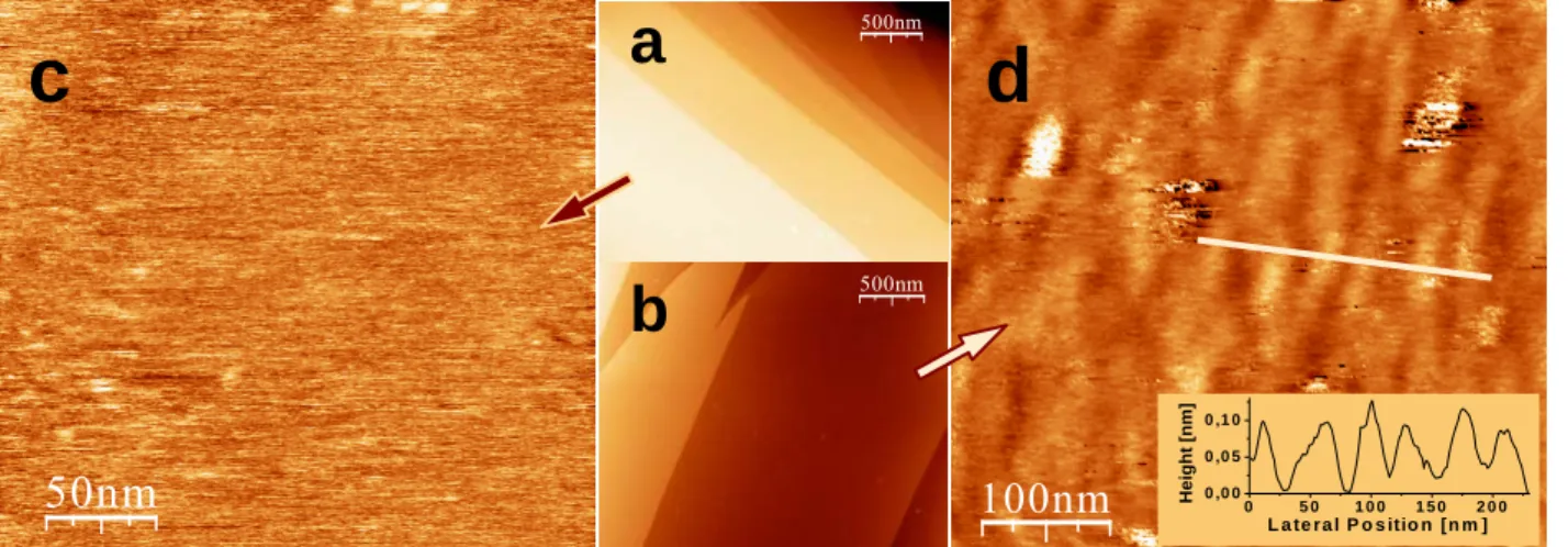
Figure 5. STM images of the surface of two cleaved GaTa4Se8 crystals. Large scale images of the pristine crystal in (a) (bias 0.76 V, IT = 0.25 nA) and of the transited crystal in (b) (bias 0.56 V, IT = 0.25 nA) reveal, in both cases, large terraces. On a nanometer scale however, clear differences are observed: While the pristine crystal surface shows no structure in (c) (bias 0.76 V, IT = 0.25 nA), the transited one displays a characteristic filamentary pattern in (d) (bias 0.44 V, IT = 0.17 nA). Inset in (d): The topography profile along the indicated line highlights the observed spatial modulation.
chalcogenides, like Ag2S,[14] or in oxides like SrTiO3,[15]
the resistive switching is related to redox processes induced by cation or anion migration, and the mechanism refers mainly to an ionic effect. For the Ge- or Sb-based telluride alloys the resistive switching is related to the amorphous-crystalline phase transition observed in these systems,[16,17] and this effect can be classified as a thermal
effect. Similarly, the resistive switch in NiO requires a high power density (≈ 1012 W/cm3)[14] and electric fields
(≈ 1 MV/cm), and was associated to the formation or destruction of Ni conductive filaments by Joule heating.[18] Finally, in manganites,[19] or Cr-doped
SrTiO3,[20] the resistive switching mechanism refers
mainly to an interfacial electronic effect. A charge doping model in which the charge injection induces an insulator metal transition close to the interface was initially proposed.[21] However, recent works on transition metal
oxides have highlighted the role of the oxygen electromigration as another possible origin for the MIT observed close to the interface. [22, 23]
None of the mechanisms describe above seems appropriate to explain the resistive switching in the Mott insulator GaTa4Se8. For this compound, the resistive
switching can be obtained with electric fields as low as 450 V/cm (sample #3, see Fig. 3) which is three orders of magnitude smaller than values required for the fuse type switching observed in NiO. Moreover, our single crystal X-ray diffraction experiments showed no changes, within our experimental resolution, in the structure of the crystal of GaTa4Se8 before and after application of pulses (see
Fig. 1).[24] The resistive switching is thus neither related to
a significant sample damage nor to drastic structural modifications such as the crystalline-amorphous transition observed in chalcogenides Phase Change Materials.[16, 17]
The resistive switching in GaTa4Se8 was also observed
using a four probes technique which is consistent with a “bulk” effect and not with an interfacial electronic effect as proposed in transition metal oxides like manganites. [21-23] Finally, contrary to Cu, Ag or O, none of the elements
Ga, Ta and Se are known to lead to high ionic
conductivity which makes redox processes induced by cation or anion migration very unlikely in GaTa4Se8.
Similarly the capacitance geometry used for sample #3 (see inset of Fig.3) invalidates the scenario of a diffusion of electrodes elements (which would require a bulk diffusion of carbon atoms over more than 40 µm) for the origin of the resistance switching.
To get a deeper insight into the microscopic nature of the pulse-induced MIT observed in GaTa4Se8, STM
measurements were performed. These experiments were undertaken on crystals cleaved in air just before their introduction into the ultra-high vacuum chamber (base pressure 2x10⁻¹⁰ mbar). The STM images revealed a
sample surface characterized by large flat terraces, observed on both, pristine (Fig. 5a) and transited (Fig. 5b) crystals. The well-defined steps clearly visible on both images have apparent height of 0.5 nm (or its multiple) corresponding to half the unit cell parameter of the material. The high-resolution STM images reveal, however, that important differences exist on a nanometer scale. Whereas the surface topography of pristine crystals is structure-less (Fig.5c), the STM images recorded on transited crystals are characterized by 30-50 nm size filamentary structures (Fig. 5d), with apparent height of ~0.1 nm, and qualitatively along the direction of the electric pulse. Such a filamentary pattern is representative of the AEP state: similar images were obtained with different STM tips in numerous locations of different transited crystals. These STM measurements indicate that the electric pulse affects somehow the bulk material as they were obtained on crystals cleaved in their AEP states. In constant-current STM images, regions with increased local density of states appear higher than regions with reduced local density of states. It is therefore not easy to distinguish a priori between real topographic structures and spectroscopic effects. However, an apparent height of ca. 0.1 nm lower than the atomic scale (ca. 0.2-0.3 nm) seems difficult to explain on the basis of pure topographic effects, and at least a part of the apparent height variations observed in Figure 5b has an
electronic origin. Thus, STM images strongly suggest the presence of an Electronic Phase Separation (EPS) in the AEP state and point to the formation of nanometer-size domains organized in a filamentary structure. It is worth noting that EPS has recently attracted great attention in transition metal oxides that exhibit strong electronic correlations as GaTa4Se8. [25-30]
Considering such an electric pulse induced EPS, the peculiar transport properties observed in GaTa4Se8
(Fig. 2) can be naturally explained. In fact, the high temperature resistance is barely affected by the electric pulse while a strong reduction of the resistance occurs at low temperature in the AEP state (see inset Fig. 2a). This suggests that electric pulses generate a small amount of new conducting channels in parallel with unaffected parts of the crystal. Since the room temperature conductivity of the unaffected parts is rather high, a small number of filament-like conducting domains would indeed not change significantly the macroscopic resistance in this temperature range. Conversely, at lower temperature where the resistance of the unaffected parts increases drastically, the filamentary domains may become the leading conductance pathways and therefore correspond to the main contribution to the AEP resistivity below 100 K. The rather high value of the low temperature resistivity (ca. 102 Ω.cm, see curve 2 in Fig. 2a) compared to usual
correlated metallic systems (typically smaller than 10-1
Ω.cm),[3] is compatible with a small volume fraction of
the conducting phase. Interestingly, the resistivity temperature dependence of this conducting phase resembles the one of granular metals. [31] This suggests
that metallic domains are discontinuous and are separated by less conducting parts. This perfectly corresponds to the STM observation of nanometer size domains and reinforces the hypothesis according to which the resistance drop observed at TC = 5-7 K results from an inhomogeneous non-percolating superconductivity.
In conclusion, we have reported the first experimental evidence that an electric pulse can induce a non-volatile insulator-to-metal transition in the Mott insulator GaTa4Se8. Our results show that the breakdown
of the Mott insulating state is concomitant with an electric-pulse-induced electronic phase separation. The peculiar metallic-like state exhibits an electronic transition at TC = 5-7 K which is presumably associated with the occurrence of a non percolative superconductivity. At this stage, a detailed microscopic picture of these phenomena is missing. The resistive switching observed in GaTa4Se8 seems quite different
from the thermal, ionic, and electronic effects leading to resistive switching in other type of materials. We can not conclude yet on whether the resistive switching observed in GaTa4Se8 is a current or a voltage effect. We note,
however, that GaTa4Se8 shows both, a pressure and an
electric pulse induced MIT, and belongs to a non centrosymmetric Space Group (F-43m) compatible with piezoelectricity. Recent theoretical calculations have shown that the electric field could affect the transfer integral (t) in a Mott insulator and possibly lead to a MIT.[4,5] In principle, for piezoelectric compounds the
transfer integral (t) could be even more affected by the
electric field. Piezoelectric (or ferroelectric) effect could therefore provide a key to the understanding of the striking electric-pulse induced MIT an concomitant EPS formation observed in the Mott insulator GaTa4Se8 . Experimental
Sample preparation : Pure powders of GaTa4Se8 were
synthesized as reported elsewhere [6-8]. Crystals of typical sizes around 300 µm were subsequently obtained by selenium transport method. The powder was placed in an evacuated silica tube with a small excess of Se and heated at 950°C for 24 hours and then slowly cooled (2°C/hour) to room temperature.
Transport measurements : The low bias resistance of the
crystals was measured using a source measure Keithley 236 with a standard 2 or 4 probes technique and different types of electrodes (Au, Ag, C).
Electric pulse were applied using an Agilent 8114A. During the pulse the voltage drop in the sample was measured with a Tektronik TDS 340 oscilloscope, and the intensity through the circuit was monitored with a load resistor inserted in series.
Description of the samples : S: section of the sample; L:
distance between injection electrodes; l: distance between bias measurement electrodes.
- Sample #1 shown in Figure 2c: four probes technique with carbon electrodes (Emerson & Cuming, Electrodag PR-406). L = 240 µm l = 60 µm S = 160 * 140 µm2.
- Sample #2 shown in Figure 2d: two probes technique with gold electrodes evaporated on the crystal and separated by 10 microns. Gold wires were contacted on top of the gold electrodes using a carbon paste. L = l = 10 µm ; S = 200 * 100 µm2
- Sample #3 shown in Figure 3: cleaved crystal measured in capacitance geometry with two carbon electrodes (pad size = 100 * 100 µm2) L = l = 40 µm ; S= 200 * 200 µm2 and .
- Sample #4 : four probes technique with carbon electrodes L = 300 µm; l = 60 µm; S = 260*200 µm2.
- Sample #5 : two probes technique with carbon electrodes L = l = 140 µm ; S = 180 * 180 µm2
Acknowledgments
The authors thank J. Martial at IMN for her help in samples preparation, and F. Debontridder at INSP for technical support. This work was supported by a Young Researcher grant ANR-05-JCJC-0123-01 from the French Agence Nationale de la Recherche (to L.C., B.C. and E.J.). L.C., B.C. and E.J contributed equally to this work. Supporting Information is available online from Wiley InterScience or from the authors. _____________________
[1] J. G. Bednorz and K. A. Muller, Z. Physik B 1986, 64, 189 [2] S. Jin, T. H. Tiefel, M. McCormack, R. A. Fastnacht, R.
Ramesh and L. H. Chen, Science 1994, 264, 413
[3] M. Imada, A. Fujimori and Y. Tokura, Rev. Mod. Phys.
1998, 70, 1039
[4] T. Oka and H. Aoki, Phys. Rev. Lett. 2005, 95, 1
[5] T. Oka, R. Arita and H. Aoki, Phys. Rev. Lett. 2003, 91, 066406
[6] R. Pocha, D. Johrendt, B. F. Ni and M. M. Abd-Elmeguid, Journal of the American Chemical Society 2005, 127, 8732-8740
[7] M. M. Abd-Elmeguid, B. Ni, D. I. Khomskii, R. Pocha, D. Johrendt, X. Wang and K. Syassen, Physical Review Letters 2004, 93, 126403
[8] H. Ben Yaich, J. C. Jegaden, M. Potel, M. Sergent, A. K. Rastogi and R. Tournier, J. Less-Common Met. 1984, 102, 9
[9] A. Asamitsu, Y. Tomioka, H. Kuwahara and Y. Tokura, Nature 1997, 388, 50
[10] S. Yamanouchi, Y. Taguchi and Y. Tokura, Phys. Rev. Let.
1999, 83, 5555
[11] L. Cario, B. Corraze, A. Meerschaut and C. O., Phys. Rev. B 2006, 73, 155116
[12] H. Chudo, C. Michioka, H. Nakamura and K. Yoshimura, Physica B 2006, 378, 1150
[13] P. Birrer, F. N. Gygax, B. Hitti, E. Lippelt, A. Schenck, M. Weber, D. Cattani, J. Cors, M. Decroux and O. Fischer, Physical Review B 1993, 48, 16589
[14] R. Waser and M. Aono, Nature Materials 2007, 6, 833 [15] K. Szot, W. Speier, G. Bihlmayer and R. Waser, Nature
Materials 2006, 5, 312
[16] M. H. R. Lankhorst, K. B.W.S.M.M. and W. R.A.M., Nature Materials 2005, 4, 347
[17] M. Wuttig and N. Yamada, Nature Materials 2007, 6, 824 [18] D. C. Kim, S. Seo, S. E. Ahn, D.-S. Suh, M. J. Lee, B.-H.
Park, I. K. Yoo, I. G. Baek, H.-J. Kim, E. K. Yim, J. E. Lee, S. O. Park, H. S. Kim, U.-I. Chung, J. T. Moon and B. I. Ryu, Applied Physics Letters 2006, 88, 202102
[19] S. Q. Liu, N. J. Wu and A. Ignatiev, Applied Physics Letters 2000, 76, 2749
[20] A. Beck, J. G. Bednorz, C. Gerber, C. Rossel and D. Widmer, Applied Physics Letters 2000, 77, 139-141 [21] M. J. Rozenberg, I. H. Inoue and M. J. Sanchez, Phys. Rev.
Let. 2004, 92, 178302
[22] I. H. Inoue, S. Yasuda, H. Akinaga and H. Takagi, Phys. Rev. B 2008, 77, 035105
[23] M. Janousch, G. I. Meijer, U. Staub, B. Delley, S. F. Karg and B. P. Andreasson, Advanced Materials 2007, 19, 2232 [24] CSD, Further details of the crystal structure investigation
may be obtained from Fachinformationszentrum Karlsruhe, 76344 Eggenstein-Leopoldshafen, Germany (fax: (+49)7247-808-666; e-mail: crysdata@fiz-karlsruhe.de, http://www.fiz-karlsruhe.de/ecid/Internet/en/DB/icsd/ depot_anforderung.html) on quoting the deposition number CSD-418017. 2007,
[25] E. Dagotto, Science 2005, 309, 257
[26] T. Cren, D. Roditchev, W. Sacks, J. Klein, J.-B. Moussy, C. Deville-Cavellin and M. Laguës, Phys. Rev. Lett. 2000, 84, 147
[27] T. Cren, D. Roditchev, W. Sack and J. Klein, Europhys. Lett. 2001, 54, 84
[28] S. H. Pan, J. P. O'Neal, R. L. Badzey, C. Chamon, H. Ding, J. R. Egelbrecht, Z. Wang, H. Eisaki, S. Uchida, A. K. Guptak, K. W. Ng, E. W. Hudson, K. M. Lang and J. C. Davis, Nature 2001, 413, 282
[29] C. Renner, G. Aeppli, B.-G. Kim, Y.-A. Soh and S. W. Cheong, Nature 2002, 416, 518
[30] Y. Tokura, Rep.Prog. Phys. 2006, 69, 797
[31] A. Gerber, A. Milner, G. Deutscher, M. Karpovsky and A. Gladkikh, Phys. Rev. Lett. 1997, 78, 4277