HAL Id: cea-01500564
https://hal-cea.archives-ouvertes.fr/cea-01500564
Submitted on 3 Apr 2017HAL is a multi-disciplinary open access
archive for the deposit and dissemination of sci-entific research documents, whether they are pub-lished or not. The documents may come from teaching and research institutions in France or abroad, or from public or private research centers.
L’archive ouverte pluridisciplinaire HAL, est destinée au dépôt et à la diffusion de documents scientifiques de niveau recherche, publiés ou non, émanant des établissements d’enseignement et de recherche français ou étrangers, des laboratoires publics ou privés.
Tunable Doping in Hydrogenated Single Layered
Molybdenum Disulfide
Debora Pierucci, Hugo Henck, Zeineb Ben Aziza, Carl H. Naylor, Adrian
Balan, Julien E. Rault, Mathieu G. Silly, Yannick J. Dappe, François Bertran,
Patrick Le Fèvre, et al.
To cite this version:
Debora Pierucci, Hugo Henck, Zeineb Ben Aziza, Carl H. Naylor, Adrian Balan, et al.. Tunable Doping in Hydrogenated Single Layered Molybdenum Disulfide. ACS Nano, American Chemical Society, 2017, 11, pp.1755 - 1761. �10.1021/acsnano.6b07661�. �cea-01500564�
Mathieu G. Silly,
Yannick J. Dappe,
François Bertran,
Patrick Le Fèvre,
Fausto Sirotti,
A. T. Charlie Johnson,
‡and Abdelkarim Ouerghi
*
,††Centre de Nanosciences et de Nanotechnologies, CNRS, Univ. Paris-Sud, Université Paris-Saclay, C2N − Marcoussis, F91460
Marcoussis, France
‡Department of Physics and Astronomy, University of Pennsylvania, 209S 33rd Street, Philadelphia, Pennsylvania 19104, United
States
§Synchrotron-SOLEIL, Saint-Aubin, BP48, F91192 Gif sur Yvette Cedex, France
∥SPEC, CEA, CNRS, Université Paris-Saclay, CEA Saclay, F91191 Gif-sur-Yvette Cedex, France
*
S Supporting InformationABSTRACT: Structural defects in the molybdenum disul-fide (MoS2) monolayer are widely known for strongly
altering its properties. Therefore, a deep understanding of these structural defects and how they affect MoS2electronic
properties is of fundamental importance. Here, we report on the incorporation of atomic hydrogen in monolayered MoS2to tune its structural defects. We demonstrate that the
electronic properties of single layer MoS2can be tuned from
the intrinsic electron (n) to hole (p) dopingvia controlled exposure to atomic hydrogen at room temperature. Moreover, this hydrogenation process represents a viable technique to completely saturate the sulfur vacancies
present in the MoS2flakes. The successful incorporation of hydrogen in MoS2leads to the modification of the electronic
properties as evidenced by high resolution X-ray photoemission spectroscopy and density functional theory calculations. Micro-Raman spectroscopy and angle resolved photoemission spectroscopy measurements show the high quality of the hydrogenated MoS2 confirming the efficiency of our hydrogenation process. These results demonstrate that the MoS2
hydrogenation could be a significant and efficient way to achieve tunable doping of transition metal dichalcogenides (TMD) materials with non-TMD elements.
KEYWORDS: n and p doped MoS2, defects, atomic hydrogenation, doping, spectroscopy, electronic properties
F
ollowing similar trend as graphene, the two-dimensional (2D) transition metal dichalcogenides (MX2) have attracted much interest recently thanks to their versatile electronic and optical properties. However, unlike graphene that does not have a bandgap, they exhibit attractive properties such as indirect-to-direct bandgap crossover with decreasing number of atomic layers and strong photoresponses.1−3 Moreover, 2D MX2 materials have interesting electronic structure, i.e., their tunable bandgap by varying the layer thickness and strain,4,5 their edge-dependent semiconducting-to-metallic transitions,6 in addition to the transformations between different S−Mo−S atoms stacking geometries (for instance, 2H to 1T phase of monolayer MoS27). In contrast tographene where only small bandgap (few hundred meV) can be opened by strain and other methods,8large bandgap tunability can be obtained with 2D MX2 where we can switch from a
semiconducting (with a few eV bandgap) to a metallic form.9
This large tunability allows broadening the applications of MX2
in nanoelectronic devices.
Furthermore, the presence of defects can induce deep gap states responsible for the intrinsic doping of these materials.10,11 For instance, in the case of MoS2, sulfur monovacancies
represent the defects with the lowest formation energy12−14and the most common generally present in MoS2 flakes.12 In
particular, these sulfur vacancies (Sv) cause the presence of unsaturated electrons in the surrounding Mo atoms and act as electrons donors15,16 responsible for the n-type doping of MoS2.17It has already been demonstrated that the intercalation of oxygen,18nitrogen,19or niobium20can reduce the intrinsic
Received: November 14, 2016 Accepted: February 1, 2017 Published: February 1, 2017
doping of MoS2. Recent experiments using mainly Raman spectroscopy and high resolution X-ray photoemission spec-troscopy (HR-XPS) demonstrated that the n doped MoS2can be tuned to p doped by N2 plasma.
21
The introduction of dopants in MoS2lattice represents a potential route to achieve stable MoS2with different functionalities. Therefore, it is crucial
to develop controllable techniques to make possible the tunability of MoS2 properties without degrading the quality
of MoS2flakes.
In this work we report an easy and effective chemical doping method by hydrogen atoms, already used as dopants for graphene22,23 and we show that hydrogen represents an effective way to passivate sulfur vacancies. We study the electronic properties of the hydrogen-doped MoS2, by exposing
the sample to atomic hydrogen gas. HR-XPS studies reveal the n type doping of pristine single layer MoS2 which is also
confirmed by the measurement of the valence band maximum (VBM). We demonstrate that the atomic hydrogen doping can tune this intrinsic n doping until reaching p doped MoS2. The analysis of the total density of states (LDOS) of the hydrogenated MoS2byfirst principle calculations using density functional theory (DFT) shows the presence of new gap states close to the VBM, confirming the p-type behavior of the hydrogenated MoS2on graphene. We also checked the quality
of the hydrogenated MoS2using angle resolved photoemission spectroscopy (ARPES) measurements, which show sharp band structures. These results confirm the validity of the doping process without a degradation of the MoS2flakes.
RESULTS AND DISCUSSION
We used p-type graphene substrate obtained by hydrogenation of epitaxial graphene. This bilayer graphene/SiC(0001) presents several advantages. The graphene/SiC is conducting therefore particularly suited for XPS/ARPES measurements.24 Also, the graphene presents a chemically inert surface due to
the strong coupling of all its pz atomic orbitals which are stabilized in a giant delocalized π bonding system.25−27 This configuration inhibits the possibility of covalent addition and then the interaction with atomic hydrogen. Moreover, the prehydrogenation treatment of the graphene/SiC substrate,28 ensures the saturation of the dangling bonds present at the SiC/buffer layer interface,22 preventing the hydrogen inter-calation in graphene during the MoS2treatment. Large (20−
100μm) MoS2flakes are grown by chemical vapor deposition (CVD) and then further deposited on the p doped bilayer graphene substrate using wet transfer process.29 To further clean the surface and interface of the MoS2/graphene
heterostructure, we annealed the samples at T = 300 °C for 30 min in ultrahigh vacuum (UHV) (P≈ 10−10mbar).30More details about the growth and sample preparation are given in theMethodssection.
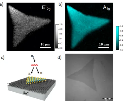
After the transfer, the quality of the MoS2flakes was verified
by Raman spectroscopy. The two Raman maps inFigure 1(a) and (b) show the intensity of the E1
2gand A1gRaman modes,
respectively, of the MoS2 on graphene layer. The two Raman peaks correspond to the in-plane vibrations (E1
2g) and out of
plane vibrations (A1g) of Mo and S atoms in the MoS2.31These maps reveal a large and uniform MoS2 flake with only some
variations of contrast in the wholeflake. This uniformity of the peaks intensities indicates the good quality of our MoS2flakes.
In order to investigate the effects of atomic hydrogen exposures to single layer MoS2 on p doped bilayer graphene/SiC, the
sample was exposed to several atomic hydrogen doses (∼5 × 10²L, 5× 10³L and 8× 10⁴L, where 1 Langmuir (L) = 10−6
Torr × s). The molecular dihydrogen was cracked by a hot tungsten filament (1400 °C, approximately 5 cm from the sample), as illustrated in the schematic of Figure 1(c).Figure 1(d) shows an optical micrograph of a representative single layerflake on graphene/SiC after the hydrogenation process.
Figure 1. (a,b) Micro-Raman maps of E1
2gand A1gpeaks of the MoS2on epitaxial graphene. (c) Schematic illustration of our current method for hydrogen-doped MoS2. (d) Typical optical image of a hydrogenated MoS2flake on epitaxial graphene/SiC.
ACS Nano Article
DOI:10.1021/acsnano.6b07661 ACS Nano 2017, 11, 1755−1761
284.3 eV. These components correspond to bulk SiC and bilayer graphene, respectively.28The shape and the position of the C 1s peak, arising from the graphene and the SiC underlayer, have not changed after the exposition to three hydrogen doses, with respect to the pristine one. This confirms that the hydrogen did not interact with the graphene/SiC underlayer. The evolution of the Mo 3d and S 2p peaks from the pristine MoS2through the three different hydrogen doses
are shown inFigure 2(a) and (b), respectively. For the pristine
MoS2, the Mo 3d spectrum contains one main doublet
component at binding energy (BE) Mo 3d5/2 = 229.7 eV (3d5/2:3d3/2 ratio of 0.66 and a spin−orbit splitting of 3.10
eV32) related to a Mo4+ in a sulfur environment33
with a trigonal prismatic phase (1H-MoS2). A smaller contribution
visible at lower BE (∼−0.52 eV) with respect to this main doublet peaks is the signature of a defective/substoichiometric MoS2with Sv.12,33The weight of this component (between 15 and 18% of the whole Mo 3d spectrum) is not representative of a single MoS2flake due to the large X-ray beam size (∼100− 150μm diameter), but it gives information on the percentage of defective MoS2in the explored area. The additional peak at BE = 226.5 eV is due to the sulfur 2s peak. The S 2p spectrum of the pristine MoS2present only one main doublet at BE S 2p3/2= 162. Five eV (2p1/2:2p3/2ratio of 0.5 and a spin−orbit
splitting of 1.19 eV32) as expected for divalent sulfide ions (S2−) in 1H-MoS2.33,34 These BE values for the Mo 3d and S 2p
indicate an intrinsic n-type doping of the MoS2flakes,15mostly induced by the Sv which act as an electron donating defects. No
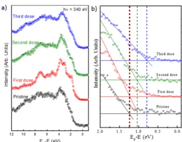
all core levels BE are shifted by−0.3 eV, indicating a complete saturation of the Sv. In this case both, the Mo 3d and S 2p peaks became sharper (fwhm = 0.6 to 0.5 eV). The saturation of these vacancies gradually reduced the n-type doping of the MoS2decreasing the distance of the VBM to the Fermi level (FL) as shown inFigure 3(a) and (b), from 1.25 eV for the
pristine MoS2to 1.05 eV (almost midgap, considering a quasi-particle bandgap of 2 eV38) for the second hydrogen dose. We notice that the spectra inFigure 3(a) show similar characteristic peaks, before and after hydrogenation (for different doses), that are related to MoS2valence band.39The shifts of hydrogenated MoS2shown inFigure 3(b) are caused by the rigid energy shift
of all core-levels. When the hydrogen dose is further increased the core level peaks still shift toward lower binding energy (−0.5 eV), which correspond to a distance of the VBM to the FL of about 0.75 eV. This means that a p-type doping is now induced in the MoS2flakes. This huge hydrogen dose (∼8 × 10⁴L) probably starts to induce new Sv, directly replaced by hydrogen forming Mo−H bonds.40−42The formations of Mo− H bonds and the saturation of the Sv replace the donor gap state present in the pristine MoS2 to new acceptor gap state related to the Mo−H bond formation as shown below by DFT calculations. Moreover, the Mo 3d and S 2p spectra show also the presence of a new component at lower binding energy with respect to the main doublet peaks (∼0.8 eV). These components are probably related to the formation of the
Figure 2. XPS measurement for MoS2at different doses of atomic hydrogen: (a) Mo-3d core level, (b) S-2p core level athν = 340 eV. The experimental data points are displayed as dots. The solid line is the envelope offitted components.
Figure 3. (a) Valence band intensity integrated spectra as a function of the binding energy of pristine MoS2and hydrogenated MoS2(for three doses). (b) Zoom of (a). The experimental data points are displayed as dots.
octahedral 1T phase of MoS2induced by the high density of
hydrogen atoms present in the sample.
The electronic structure and the stability of the hydrogenated MoS2, kept one month under ambient conditions after the
hydrogenation (a dose of 5 × 10³ L), were studied using
ARPES (Figure 4). Figures 4(a) and (b) show the ARPES momentum energy image, before and after hydrogenation respectively, around the Γ point of the Brillouin zone (BZ). The expected signal of the monolayer MoS2 valence band is visible.43,44The shape of the upper band of the valence bands is not modified but only shifted toward the FL because of the exposure to the hydrogen atoms. Moreover, we notice the same shift for the other bands around−3 eV and −4 eV (highlighted by the white circles). Hence, we can claim that the hydrogenation induces a uniform shift of all the bands forming the valence bandstructure of MoS2. The sharp and intense
experimental band structure of Figure 4(b) confirms the hydrogenation process preserves the high structural quality of the MoS2 flakes. The ARPES quality is even better after hydrogenation suggesting that the hydrogen treatment improves the surface quality of the MoS2by passivating the Sv.
ARPES measurement, perpendicular to theΓ−K direction of the p-doped graphene underlayer BZ before and after the hydrogenation of MoS2/p-doped graphene underlayer, are shown in the Supporting Information in Figure S2. In this intensity map, the graphene underlayer presents twoπ bands, which is the clear signature of the interlayer decoupling induced by the hydrogenation of the epitaxial graphene giving rise to a quasi-free-standing bilayer graphene and a completely saturated SiC surface. Moreover, in this sample orientation, the two branches of the grapheneπ bands can be observed45allowing the determination of the Dirac point position with respect to the FL. Close inspection of the dispersion relation around K reveals that the FL is located at 0.25 eV below the Dirac points for the pristine MoS2/graphene heterostructure and is not
modified after the hydrogen dose. This value corresponds to a hole doping level of the graphene underlayer of about 3.8 × 1012cm−2.
In order to probe the effects of atomic hydrogen on the electronic properties of hydrogen doped MoS2(8× 10⁴L), we
performed micro-Raman spectroscopy on twoflakes with the same orientation angle with respect to the graphene underlying substrate. This choice is made so that we can assume that the flakes are subjected to the same orientation-induced strain.38,46,47InFigure 4(c), the Raman spectra of MoS2before
and after the hydrogenation are shown. The two vibrational modes are separated by about 19 cm−1which corresponds to a single layered MoS2as was reported for MoS2monolayer.48,49 After the treatment, we clearly observe that a downshift of the E12g peak has occurred together with a splitting of this peak.
This is likely due to a strain induced by the hydrogen intercalation (which is probably responsible for the appearance of the 1T-phase);50 this strain is tensile as indicated by the direction of the E1
2gshift.
47,51−53
The peak splitting gave rise to two distinctive E12gmodes, similarly to what was observed by A.
Azcatl et al., who doped the MoS2 using nitrogen plasma.
21
Furthermore, the A1g peak is slightly upshifted which can be explained by a change of the doping level in MoS2,38,54i.e., the
saturation of the Sv, the hydrogen atoms introduction, and eventually the removal of S atoms.14,55On the other hand, the increase of the A1gpeak intensity or in other words the increase
of the ratio of intensities A1g/E12gis consistent with what was
reported on the p doping of MoS2.20According to these Raman results, we show that the hydrogenation of MoS2 was successfully done leading to a nondefective MoS2.
Photo-luminescence (PL) spectra of pristine and hydrogenated MoS2
are provided in Figure S3. We notice that the PL intensity decreases after hydrogenation; this PL quenching can be explained by the suppression of defects from MoS2 at room
temperature as was observed for pristine and irradiated MoS2.14 This confirms again that the used process is noninvasive and that it is possible to hydrogenate MoS2even with better quality.
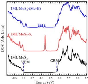
In order to gain insights into this doping change from n to p of the MoS2 flakes we performed first principle calculations
based on DFT.Figure 5shows the total density of state (DOS) of a perfect MoS2monolayer (black curve), MoS2with Sv (red curve) and Sv saturated by hydrogen atoms (blue curve). As expected, the presence of Sv induces defect state in the gap, located at about 0.75 eV below the conduction band minimum (CBM). This donor state is in fact responsible for the intrinsic n-type doping of the pristine MoS2flake as measured by XPS.
Our calculation shows that Mo−H bonds induce new gap state at about 0.16 eV above the valence band maximum (VBM). The presence of this acceptor like state confirms the p-type behavior observed experimentally after the MoS2 hydro-genation. The combination of XPS experiments and DFT gives a global picture of the structural and electronic MoS2
properties after the hydrogenation process. A single layer MoS2 includes well-known Sv as displayed in Figure 6(a). After the first hydrogenation (Figure 6(b)), the hydrogen atoms react
Figure 4. (a,b) ARPES measurements at room temperature of pristine MoS2/graphene at hν = 50 eV and hydrogenated MoS2/graphene heterostructure athν = 100 eV, respectively along the graphene ΓK direction. The Fermi level position is located at the zero of the binding energy (marked as a white dashed line), the white circles highlight the shift in the position of the band located at around−4 eV. (c) Comparison between the Raman spectra of MoS2before (in black line) and after (in blue line) hydrogenation.
ACS Nano Article
DOI:10.1021/acsnano.6b07661 ACS Nano 2017, 11, 1755−1761
with the unbound Mo atoms. This model explains the elimination of defect peaks in Mo 3d. At high atomic hydrogen dose, if new Sv vacancies are created by high hydrogen dose, they are readily replaced by the hydrogen atoms increasing the p-type doping of the MoS2as indicated by the energy shift of the Mo-3d and S-2p core level spectra toward lower binding energy and the reduction of the energy distance of the VBM with respect to the FL upon hydrogenation (Figure 6(c)).
CONCLUSIONS
In summary, we conducted a comprehensive study of the interaction of atomic hydrogen with monolayer MoS2. The
pristine MoS2has sulfur vacancies, which are responsible for its
intrinsic n-type doping. During hydrogen dosing, the hydrogen atoms react with the under-coordinated Mo atomsfilling the Sv. When all the vacancies arefilled, the MoS2becomes almost
intrinsic (VBM = 1.05 eV). At higher atomic hydrogenation, the hydrogen breaks the Mo−S bonds and passivates the newly created vacancies inducing a p-type doping in the MoS2sample. This model suggested by the HR-XPS results is corroborated by DFT calculations predicting the presence of an acceptor gap
by thermal heating the SiC(0001) substrate. Before the graphitization, the substrate was etched with hydrogen (100% H2) at 1550 °C to produce well-ordered atomic terraces of SiC. The substrate was heated to 1000 °C and then further heated at 1550 °C under argon (800 mbar).
Growth and Transfer of MoS2. Large scale MoS2 monolayer flakes (≈20 to ≈100 μm) have been grown by Chemical Vapor Deposition (CVD) on oxidized silicon substrate (see ref 56). The MoS2 flakes transferred onto the graphene retain their triangular shapes with unchanged lateral sizes. Before any measurement, the MoS2sample was annealed at 300°C for 30 min in ultrahigh vacuum (P ≈ 10−10 mbar), in order to remove the residual surface contaminations induced by the wet transfer.
Atomic Hydrogen Doping. The hydrogenation process has been performed at room temperature under a pressure of 2× 10⁻⁵mbar of H2 in order to avoid hydrogen etching of the MoS2 layer. The hydrogenation process lasted 3 h, under a lower pressure of H2, in order to control the phenomena that may occur on the MoS2 properties. This procedure has been repeated twice, after each the sample was fully characterized by means of XPS measurements.
HR-XPS. HR-XPS experiments were carried out on the TEMPO beamline57 (SOLEIL French synchrotron facility) at room temper-ature. The photon source was a HU80 Apple II undulator set to deliver horizontally linearly polarized light. The photon energy was selected using a high-resolution plane grating monochromator, with a resolving power E/ΔE that can reach 15 000 on the whole energy range (45−1500 eV). During the XPS measurements, the photo-electrons were detected at 0° from the sample surface normal n⃗ and at 46° from the polarization vector E⃗. The spot size was 80 × 40 (H × V) μm2.
A Shirley background was subtracted in all core level spectra. The C 1s spectrum wasfitted by a sum of a Gaussian function convoluted with a Doniach-Sunjic line shape. An asymmetry factorα was used, whereα = 0.1 eV (G peak) and α = 0 eV (SiC). The Mo 3d and S 2p spectra werefitted by sums of Voigt curves, i.e., the convolution of a Figure 5. Total DOS of pristine MoS2 (black line), MoS2with Sv
(red line), and hydrogenated MoS2 (blue line) using DFT calculations.
Figure 6. Band diagram showing the evolution of MoS2Fermi level (a) before hydrogenation, (b) upon thefirst exposure to hydrogen, and (c) after the complete hydrogenation.
Gaussian (of width at half-maximum GW) by a Lorentzian (of full-width at half-maximum LW). The LW wasfixed at 90 meV for Mo 3d and S 2p.32
Angle-Resolved Photoemission Spectroscopy. The ARPES measurements were conducted at the CASSIOPEE beamline of Synchrotron SOLEIL (Saint-Aubin, France). We used horizontally linearly polarized photons of 50 eV and a hemispherical electron analyzer with vertical slits to allow band mapping. The total angle and energy resolutions were 0.25° and 25 meV. The mean diameter of the incident photon beam was smaller than 50 μm. All ARPES experiments were done at room temperature.
DFT Calculations. First-principles calculations have been performed using a very efficient DFT localized orbital molecular dynamic technique (FIREBALL).58,59Basis sets of sp3d5 for S and Mo were used with cutoff radii (in atomic units) s = 3.9, p = 4.5, d = 5.0 (S) and s = 5.0, p = 4.5, d = 4.8 (Mo).47 In this study we have considered a standard (5 × 5) unit cell of MoS2 that has been optimized as a pristine, with an S vacancy and with an H-filled S vacancy, before calculating the corresponding DOS.
ASSOCIATED CONTENT
*
S Supporting InformationThe Supporting Information is available free of charge on the
ACS Publications websiteat DOI:10.1021/acsnano.6b07661. Figures S1−S3 (PDF) AUTHOR INFORMATION Corresponding Author *E-mail:abdelkarim.ouerghi@lpn.cnrs.fr. ORCID Abdelkarim Ouerghi:0000-0002-1898-2765 Notes
The authors declare no competingfinancial interest.
ACKNOWLEDGMENTS
This work was supported by the ANR H2DH grants. C.H.N. and A.T.C.J. acknowledge support from the National Science Foundation EFRI-2DARE program, grant number ENG-1542879.
REFERENCES
(1) Furchi, M. M.; Polyushkin, D. K.; Pospischil, A.; Mueller, T. Mechanisms of Photoconductivity in Atomically Thin MoS2. Nano Lett. 2014, 14 (11), 6165−6170.
(2) Buscema, M.; Island, J. O.; Groenendijk, D. J.; Blanter, S. I.; Steele, G. a; van der Zant, H. S. J.; Castellanos-Gomez, A. Photocurrent Generation with Two-Dimensional van Der Waals Semiconductors. Chem. Soc. Rev. 2015, 44 (11), 3691−3718.
(3) Lopez-Sanchez, O.; Lembke, D.; Kayci, M.; Radenovic, A.; Kis, A. Ultrasensitive Photodetectors Based on Monolayer MoS2. Nat. Nanotechnol. 2013, 8 (7), 497−501.
(4) Splendiani, A.; Sun, L.; Zhang, Y.; Li, T.; Kim, J.; Chim, C. Y.; Galli, G.; Wang, F. Emerging Photoluminescence in Monolayer MoS2. Nano Lett. 2010, 10 (4), 1271−1275.
(5) Conley, H. J.; Wang, B.; Ziegler, J. I.; Haglund, R. F.; Pantelides, S. T.; Bolotin, K. I. Bandgap Engineering of Strained Monolayer and Bilayer MoS 2. Nano Lett. 2013, 13 (8), 3626−3630.
(6) Li, Y.; Tongay, S.; Yue, Q.; Kang, J.; Wu, J.; Li, J. Metal to Semiconductor Transition in Metallic Transition Metal Dichalcoge-nides. J. Appl. Phys. 2013, 114, 174307.
(7) Tang, Q.; Jiang, D. Stabilization and Band-Gap Tuning of the 1T-MoS 2 Monolayer by Covalent Functionalization. Chem. Mater. 2015, 27, 3743−3748.
(8) Pierucci, D.; Sediri, H.; Hajlaoui, M.; Velez-fort, E.; Dappe, Y. J.; Silly, M. G.; Belkhou, R.; Shukla, A.; Sirotti, F.; Gogneau, N.; Ouerghi,
A. Self-Organized Metal− Semiconductor Epitaxial Graphene Layer on off-Axis 4H-SiC (0001). Nano Res. 2015, 8 (3), 1026−1037.
(9) Li, Y.; Duerloo, K.-A. N.; Wauson, K.; Reed, E. J. Structural Semiconductor-to-Semimetal Phase Transition in Two-Dimensional Materials Induced by Electrostatic Gating. Nat. Commun. 2016, 7, 10671.
(10) Krivosheeva, A. V.; Shaposhnikov, V. L.; Borisenko, V. E.; Lazzari, J. Theoretical Study of Defect Impact on Two-Dimensional MoS 2. J. Semicond. 2015, 36 (12), 122002.
(11) Lin, Z.; Carvalho, B. R.; Kahn, E.; Lv, R.; Rao, R.; Terrones, H. Defect Engineering of Two-Dimensional Transition Metal Dichalco-genides. 2D Mater. 2016, 3, 22002.
(12) Zhou, W.; Zou, X.; Najmaei, S.; Liu, Z.; Shi, Y.; Kong, J.; Lou, J. Intrinsic Structural Defects in Monolayer Molybdenum Disul Fi de. Nano Lett. 2013, 13 (6), 2615−2622.
(13) Liu, D.; Guo, Y.; Fang, L.; Robertson, J.; Liu, D.; Guo, Y.; Fang, L.; Robertson, J. Sulfur Vacancies in Monolayer MoS2 and Its Electrical Contacts. Appl. Phys. Lett. 2013, 103, 183113.
(14) Parkin, W. M.; Balan, A.; Liang, L.; Das, P. M.; Lamparski, M.; Carl, H.; Rodríguez-manzo, J. A.; Johnson, A. T. C.; Meunier, V.; Drndic, M. Raman Shifts in Electron-Irradiated Monolayer MoS 2. ACS Nano 2016, 10 (4), 4134−4142.
(15) Addou, R.; Mcdonnell, S.; Barrera, D.; Guo, Z.; Azcatl, A.; Wang, J.; Zhu, H.; Hinkle, C. L.; Quevedo-lopez, M.; Alshareef, H. N.; Colombo, L.; Hsu, J. W. P.; Wallace, R. M. Impurities and Electronic Property Variations of Natural MoS 2 Crystal Surfaces. ACS Nano 2015, 9, 9124−9133.
(16) González, C.; Biel, B.; Dappe, Y. J. Theoretical Characterisation of Point Defects on a MoS2Monolayer by Scanning Tunnelling Microscopy. Nanotechnology 2016, 27, 105702.
(17) Guo, Y.; Liu, D.; Robertson, J. Chalcogen Vacancies in Monolayer Transition Metal Dichalcogenides and Fermi Level Pinning at Contacts. Appl. Phys. Lett. 2015, 106 (17), 48−53.
(18) Nan, H.; Wang, Z.; Wang, W.; Liang, Z.; Lu, Y.; Chen, Q.; He, D.; Tan, P.; Miao, F.; Wang, X.; Wang, J.; Ni, Z. Strong Photoluminescence Enhancement of MoS2 through Defect Engineer-ing and Oxygen BondEngineer-ing. ACS Nano 2014, 8 (6), 5738−5745.
(19) Qin, S.; Lei, W.; Liu, D.; Chen, Y. In-Situ and Tunable Nitrogen-Doping of MoS 2 Nanosheets. Sci. Rep. 2014, 4, 7582.
(20) Laskar, M. R.; Nath, D. N.; Ma, L.; Ii, E. W. L.; Lee, C. H.; Kent, T.; Yang, Z.; Mishra, R.; Roldan, M. A.; Idrobo, J.; Pantelides, S. T.; Pennycook, S. J.; Myers, C.; Wu, Y.; Rajan, S.; Idrobo, J.; Pantelides, S. T.; Pennycook, S. J. P-Type Doping of MoS2 Thin Films Using Nb. Appl. Phys. Lett. 2014, 92104, 104−108.
(21) Azcatl, A.; Qin, X.; Prakash, A.; Zhang, C.; Cheng, L.; Wang, Q.; Lu, N.; Kim, M. J.; Kim, J.; Cho, K.; Hinkle, C. L.; Appenzeller, J.; Wallace, R. M. Covalent Nitrogen Doping and Compressive Strain in MoS 2 by Remote N 2 Plasma Exposure. Nano Lett. 2016, 16 (9), 5437−5443.
(22) Pallecchi, E.; Lafont, F.; Cavaliere, V.; Schopfer, F.; Mailly, D.; Poirier, W.; Ouerghi, A. High Electron Mobility in Epitaxial Graphene on 4H-SiC(0001) via Post-Growth Annealing under Hydrogen. Sci. Rep. 2014, 4, 4558.
(23) Robinson, J. A.; Hollander, M.; Labella, M.; Trumbull, K. A.; Cavalero, R.; Snyder, D. W. Epitaxial Graphene Transistors: Enhancing Performance via Hydrogen. Nano Lett. 2011, 11, 3875− 3880.
(24) Henck, H.; Pierucci, D.; Ben Aziza, Z.; Silly, M. G.; Gil, B.; Sirotti, F.; Cassabois, G.; Ouerghi, A. Stacking Fault and Defects in Single Domain Multilayered Hexagonal Boron Nitride. Appl. Phys. Lett. 2017, 110 (2), 23101.
(25) Yan, L.; Zheng, B.; Zhao, F.; Li, S.; Gao, X.; Xu, B.; Weiss, S.; Zhao, Y. Chem Soc Rev Chemistry and Physics of a Single Atomic Layer: Strategies and Challenges for Functionalization of Graphene and Graphene-Based Materials. Chem. Soc. Rev. 2012, 41, 97−114.
(26) Pallecchi, E.; Ridene, M.; Kazazis, D.; Mathieu, C.; Schopfer, F.; Poirier, W.; Mailly, D.; Ouerghi, A. Observation of the Quantum Hall Effect in Epitaxial Graphene on SiC(0001) with Oxygen Adsorption. Appl. Phys. Lett. 2012, 100 (25), 253109.
ACS Nano Article
DOI:10.1021/acsnano.6b07661 ACS Nano 2017, 11, 1755−1761
(30) Pierucci, D.; Henck, H.; Avila, J.; Balan, A.; Naylor, C. H.; Patriarche, G.; Dappe, Y. J.; Silly, M. G.; Sirotti, F.; Johnson, A. T. C.; Asensio, M. C.; Ouerghi, A. Band Alignment and Minigaps in Monolayer MoS2-Graphene van Der Waals Heterostructures. Nano Lett. 2016, 16 (7), 4054−4061.
(31) Boukhicha, M.; Calandra, M.; Measson, M. A.; Lancry, O.; Shukla, A. Anharmonic Phonons in Few-Layer MoS2: Raman Spectroscopy of Ultralow Energy Compression and Shear Modes. Phys. Rev. B: Condens. Matter Mater. Phys. 2013, 87, 195316.
(32) Mattila, S.; Leiro, J. a.; Heinonen, M.; Laiho, T. Core Level Spectroscopy of MoS2. Surf. Sci. 2006, 600 (24), 5168−5175.
(33) Kim, I. S.; Sangwan, V. K.; Jariwala, D.; Wood, J. D.; Park, S.; Chen, K.; Shi, F.; Ruiz-zepeda, F.; Ponce, A.; Jose, M.; Dravid, V. P.; Marks, T. J.; Hersam, M. C.; Lincoln, J. Influence of Stoichiometry on the Optical and Electrical Properties of Chemical Vapor Deposition Derived MoS 2. ACS Nano 2014, 8 (10), 10551−10558.
(34) Eda, G.; Yamaguchi, H.; Voiry, D.; Fujita, T.; Chen, M.; Chhowalla, M. Photoluminescence from Chemically Exfoliated MoS2. Nano Lett. 2011, 11 (12), 5111−5116.
(35) Levasseur, a; Vinatier, P.; Gonbeau, D. X-Ray Photoelectron Spectroscopy: A Powerful Tool for a Better Characterization of Thin Film Materials. Bull. Mater. Sci. 1999, 22 (3), 607−614.
(36) Baker, M. A.; Gilmore, R.; Lenardi, C.; Gissler, W. XPS Investigation of Preferential Sputtering of S from MoS 2 and Determination of MoS X Stoichiometry from Mo and S Peak Positions. Appl. Surf. Sci. 1999, 150, 255−262.
(37) Fleischauer, P. D.; Lince, J. R. A Comparison of Oxidation and Oxygen Substitution in MoS 2 Solid Film Lubricants. Tribol. Int. 1999, 32, 627−636.
(38) Liu, X.; Balla, I.; Bergeron, H.; Campbell, G. P.; Bedzyk, M. J.; Hersam, M. C. Rotationally Commensurate Growth of MoS2 on Epitaxial Graphene. ACS Nano 2015, 10 (1), 1067−1075.
(39) Han, S. W.; Cha, G. B.; Frantzeskakis, E.; Razado-Colambo, I.; Avila, J.; Park, Y. S.; Kim, D.; Hwang, J.; Kang, J. S.; Ryu, S.; Yun, W. S.; Hong, S. C.; Asensio, M. C. Band-Gap Expansion in the Surface-Localized Electronic Structure of MoS 2(0002). Phys. Rev. B: Condens. Matter Mater. Phys. 2012, 86, 115105.
(40) Search, H.; Journals, C.; Contact, A.; Iopscience, M.; Phys, S. S.; Address, I. P. The Vibration Spectrum of Hydrogen Bound by Molybdenum Sulphide Catalysts. J. Phys. C: Solid State Phys. 1981, 14, 4969−4983.
(41) Cristol, S.; Paul, J. F.; Payen, E.; Hutschka, F. Theoretical Study of the MoS 2 (100) Surface: A Chemical Potential Analysis of Sulfur and Hydrogen Coverage. J. Phys. Chem. B 2000, 104, 11220−11229.
(42) Spirko, J. A.; Neiman, M. L.; Oelker, A. M.; Klier, K. Electronic Structure and Reactivity of Defect MoS 2 II. Bonding and Activation of Hydrogen on Surface Defect Sites and Clusters. Surf. Sci. 2004, 572, 191−205.
(43) Coy Diaz, H.; Avila, J.; Chen, C.; Addou, R.; Asensio, M. C.; Batzill, M. Direct Observation of Interlayer Hybridization and Dirac Relativistic Carriers in Graphene/MoS2 van Der Waals Hetero-structures. Nano Lett. 2015, 15 (2), 1135−1140.
(44) Pierucci, D.; Henck, H.; Naylor, C. H.; Sediri, H.; Lhuillier, E.; Balan, A.; Rault, J. E.; Dappe, Y. J.; Bertran, F.; Le Févre, P.; Johnson, A. T. C.; Ouerghi, A. Large Area Molybdenum Disulphide-Epitaxial
(48) Li, H.; Zhang, Q.; Yap, C. C. R.; Tay, B. K.; Edwin, T. H. T.; Olivier, A.; Baillargeat, D. From Bulk to Monolayer MoS 2: Evolution of Raman Scattering. Adv. Funct. Mater. 2012, 22 (7), 1385−1390.
(49) Lee, C.; Yan, H.; Brus, L. E.; Heinz, T. F.; Hone, Ḱ. J.; Ryu, S. Anomalous Lattice Vibrations of Single-and Few-Layer MoS2. ACS Nano 2010, 4 (5), 2695−2700.
(50) Han, S. W.; Yun, W. S.; Lee, J. D.; Hwang, Y. H.; Baik, J.; Shin, H. J.; Lee, W. G.; Park, Y. S.; Kim, K. S. Hydrogenation-Induced Atomic Stripes on the 2 H -MoS 2 Surface. Phys. Rev. B: Condens. Matter Mater. Phys. 2015, 241303, 1−5.
(51) Wang, Y.; Cong, C.; Qiu, C.; Yu, T. Raman Spectroscopy Study of Lattice Vibration and Crystallographic Orientation of Monolayer mos2 under Uniaxial Strain. Small 2013, 9 (17), 2857−2861.
(52) Hui, Y. Y.; Liu, X.; Jie, W.; Chan, N. Y.; Hao, J.; Hsu, Y. T.; Li, L. J.; Guo, W.; Lau, S. P. Exceptional Tunability of Band Energy in a Compressively Strained Trilayer. ACS Nano 2013, 7 (8), 7126−7131. (53) Nayak, A. P.; Bhattacharyya, S.; Zhu, J.; Liu, J.; Wu, X.; Pandey, T.; Jin, C.; Singh, A. K.; Akinwande, D.; Lin, J. Pressure-induced semiconducting to metallic Transition in Multilayered Molybdenum Disulphide. Nat. Commun. 2014, 5, 3731.
(54) Chakraborty, B.; Bera, A.; Muthu, D. V. S.; Bhowmick, S.; Waghmare, U. V.; Sood, A. K. Symmetry-Dependent Phonon Renormalization in Monolayer MoS 2 Transistor. Phys. Rev. B: Condens. Matter Mater. Phys. 2012, 85 (16), 2−5.
(55) Kim, B. H.; Park, M.; Lee, M.; Baek, S. J.; Jeong, H. Y.; Choi, M.; Chang, S. J.; Hong, W. G.; Kim, T. K.; Moon, H. R.; Park, W.; Park, N.; Jun, Y. RSC Advances Structure of MoS2 Induced by Molecular Hydrogen Treatment at Room Temperature. RSC Adv. 2013, 3, 18424−18429.
(56) Han, G. H.; Kybert, N. J.; Naylor, C. H.; Lee, B. S.; Ping, J.; Park, J. H.; Kang, J.; Lee, S. Y.; Lee, Y. H.; Agarwal, R.; Johnson, a T. C. Seeded Growth of Highly Crystalline Molybdenum Disulphide Monolayers at Controlled Locations. Nat. Commun. 2015, 6, 6128.
(57) Polack, F.; Silly, M.; Chauvet, C.; Lagarde, B.; Bergeard, N.; Izquierdo, M.; Chubar, O.; Krizmancic, D.; Ribbens, M.; Duval, J.-P.; Basset, C.; Kubsky, S.; Sirotti, F.; Garrett, R.; Gentle, I.; Nugent, K.; Wilkins, S. TEMPO: A New Insertion Device Beamline at SOLEIL for Time Resolved Photoelectron Spectroscopy Experiments on Solids and Interfaces. AIP Conf. Proc. 2009, 1234 (2010), 185−188.
(58) Lewis, J. P.; Jelínek, P.; Ortega, J.; Demkov, A. A.; Trabada, D. G.; Haycock, B.; Wang, H.; Adams, G.; Tomfohr, J. K.; Abad, E.; Wang, H.; Drabold, D. A. Advances and Applications in the FIREBALL Ab Initio Tight-Binding Molecular-Dynamics Formalism. Phys. Status Solidi Basic Res. 2011, 248 (9), 1989−2007.
(59) Jelínek, P.; Wang, H.; Lewis, J.; Sankey, O.; Ortega, J. Multicenter Approach to the Exchange-Correlation Interactions in Ab Initio Tight-Binding Methods. Phys. Rev. B: Condens. Matter Mater. Phys. 2005, 71, 235101.