Economic Potential of High Density Data Storage Implemented by Patterned Magnetic Media Technology
By Lei Du
B. Eng. Materials Engineering Nanyang Technological University
MASSACHL.•ETTS INSTITUTE
OF TECHNOLOGY
SEP
1 2
2008
LIBRARIES
SUBMITTED TO THE
DEPARTMENT OF MATERIALS SCIENCE AND ENGINEERING
IN PARTIAL FULFILLMENT OF THE REQUIREMENTS FOR THE DEGREE OF MASTER OF ENGINEERING IN MATERIALS SCIENCE AND ENGINEERING
AT THE
MASSACHUSETTS INSTITUTE OF TECHNOLOGY SEPTEMBER, 2008
© 2008 Massachusetts Institute of Technology All right reserved
Signature of Author...
.--Department of Materials Science and Engineering August 15, 2008
C ertified by... .-...---... . ...
Caroline A. Ross Professor of Materials Science and Engineering Thesis Supervisor
Accepted by ... ...---
...--Samuel M. Allen POSCO Professor of Physical Metallurgy Chair, Departmental Committee on Graduate Student 9E8Wws
Economic Potential of High Density Data Storage Implemented
by Patterned Magnetic Media Technology
By Lei Du
Abstract
Hard drive industry is facing scaling challenge for areal density to be further increased. This is due to the triangular conflictions among thermal stability (superparamagnetic effect), single-to-noise ratio and writability of the recording media. One of the most promising methods to overcome this constraint is the patterned magnetic media technology. Although it is facing many challenges, the large potential gains in density offered by patterned media make it one of the possible milestones on the horizon for future of the disk drives industry. One of the biggest challenges for patterned media is to realize its mass fabrication provided reduced cost per bit. The basic fabrication approach
is to use lithography to pattern the magnetic materials on the platter. However, patterned media requires well-ordered nanoarrays with dimensions less than 25 nm, which challenges the state-of-art lithography technologies.
This M. Eng. project focuses on evaluations of the technologies and fabrication schemes potential for patterned media from various aspects like technical barriers, cost and intellectual properties. Technologies including E-beam lithography, nanoimprint lithography, templated diblock copolymer self-assembly and self-assembled magnetic nanoparticles are discussed. Cost modeling was done to prove the enormous gain in revenue for the proposed fabrication scheme. It is proposed that the fabrication scheme of templated diblock copolymer for making the master stamp for nanoimprint followed by nanoimprint lithography for mass production has the largest potential for patterned media. However, more R & D is needed for templated self-assembly of diblock copolymer before it is ready for this application. E-beam lithography which is a mature technology can also be a choice for making the stamp followed by mass production enabled by nanoimprint lithography, without a significant loss of gain in revenue for ultra-high-density media fabrications. Although the cost of a master stamp fabricated by E-beam is estimated to be 50 times more than for templated self-assembly of diblock copolymer
lithography.
Thesis advisor: Caroline A. Ross
Acknowledgements
The successful completion of this thesis is due to the contribution and help from many people. First of all, I would like to thank my thesis advisor Prof. Caroline A. Ross for her consistent guidance and help. I still remember the discussion about my thesis with her during her visit in Singapore for conference. She was always there when I had questions. Thanks to her patience and clear guidance, my problems were always solved timely. She also made me feel very comfortable in her group and I am proud that I have been a member of Ross's group. Best wishes to all the group members!
Next, I would like to thank S.N. Piramamnayagam from Data Storage Institute, Singapore. We had several discussions and he answered a lot of my queries. He also provided me useful information about magnetic recording systems and shared with me some of his perspectives on this project. Thank you very much for your sharing and help.
Also, I want to thank Prof. Eugene A. Fitzgerald for his guidance in course 3.207: Technology Development and Evaluation, which provides a useful template of technology evaluation for doing this project.
All the best to all the Master of Engineering students of 2008 class! Thank all of you for being companions for one-year study and being my friends for life. Thank Manyin for helpful discussion and suggestions about my project. And special thanks to my groupmate - Anay, with whom I could share and discuss about the technical questions in detail anytime.
Cliff, thank you. You are not only providing me important emotional support, but also always being there for me on any problem I have. I feel so grateful to God for knowing you. You will surely do great for your PHD research projects and also future careers!
I could not end without thanks to my parents, who are always supporting me, loving me and never give up me. I can not express how lucky I feel to have such a blissful family. Wish both of you healthy and let us meet soon.
Table of Contents
Abstract ... .... ... .... ... ... ... ... 2 Acknowledgement...3.... Table of Contents... ... 4 1. Introduction... ... 6 PART I: TECHNOLOGIES...72. Description of Patterned Media Technology...7
2.1. Magnetic Recording - Materials and Recording Mechanisms...7
2.2. Magnetic Properties vs. Magnet Size ... ... 10
2.3. Limitations of Conventional Media and Superparamagnetic Effect... 12
2.4. Patterned Media and Technical Barriers for Its Implementation...14
3. Competing Technologies... ... ... 16
3.1. Heat Assisted Magnetic Recording...16
3.2. Flash/Solid State Drive... ... 17
4. Fabrication Methods... ... 18
4.1. Lithography Patterned Media...18
4.1.1. Conventional lithography techniques ... 19
4.1.2. Templated self-assembly of diblock copolymer lithography ...23
4.2. Self-Assembled Nanomagnets Patterned Media/Nanocrystal Superlattice...28
5. Comparisons of Technologies and Possible Fabrication Schemes... 29
5.1. Technique 1) and 2)... ... 30
PART II: COST, IP & BUSINESS MODEL...34
6. Cost Estimations and Comparisons for Fabrication Schemes...34
6.1. Comparison of Cost: Scheme B) vs. Scheme A) - Templated Diblock Copolymer Self-Assembly vs. SEBL... 34
6.2. Comparison of Cost: Scheme B) vs. Scheme C) - Diblock Copolymer vs. Magnetic Nanoparticles ... 35
6.3. Proposed Fabrication Scheme: Scheme B) ... ... 36
6.4. Cost Modeling for Scheme B) ... ... 38
7. Patents Relevant to Patterned Media and Fabrication Methods...39
8. Value Chain and Business Model. ... 42
8.1. Structure of HDD Value Chain and Our Value Proposition ... 42
8.2. Globalization of HDD Value Chain ... ...43
8.3. Current HDD Market and Top Players ... 44
8.4. Proposed Business Model and SWOT Analysis ... 46
9. Conclusions... 49
References...51
Appendices ... 56
Appendix 1: Trends and future prediction of HDD industry... ... 56
Appendix 2: Comparisons of SSD and HDD ... 57
Appendix 3: SEBL parameters ... 59
Appendix 4: JBX-9300FS EBL system specification and charge...61
Appendix 5: Patent on patterning/lithography by self-assembly of block copolymers ...62
Appendix 6: Patent on patterned media... ... 63
Appendix 7: Toshiba's pattern on patterned media and fabrication method of forming islands in tracks/grooves ... 64
1. Introduction
The hard disk drive (HDD) industry has a history of more than fifty years and the future is predicted to be bright by industry analysts such as Gartner, IDC and TrendFOCUS. According to iSuppli', the annual revenue of HDD industry in 2007 was 32.8 billion dollars, which increased 4.6% compared to 2006 and the shipped units passed half billion in 2007 [2]. TrendFOCUS also predicted that the shipments would reach 750 million drives in 2010 [3]. The HDD industry has achieved annual increases in areal density approximately 60% in average since 1997, which exceeds Moore's Law for semiconductor industry (refer to appendix 1).
Although HDD industry is a robust industry with high revenue, it is facing scaling limitation problem together with the threat from flash/solid state memories. In order to further scaling down and increase the storage density, we must overcome the limitation imposed by the superparamagnetic effect, which occurs when the microscopic magnetic grains of the disk are reduced to so small size that ambient temperature can reverse their magnetic orientations, corrupt data and thus the storage device is unreliable and unusable. One of the most promising methods to overcome this constraint is patterned magnetic media technology [4]. Although there are many challenges in this technology, the large potential gains in density offered by patterned media make it one of the potential new milestones in the future of HDD industry. One common approach proposed by researchers is using nanolithography to pattern the magnetic platter of the disk. Major data storage companies such as Seagate, Hitachi and Toshiba, are devoting themselves
intensely into patterned media technology and launched projects on it.
However, real implementation of patterned media in HDD application is facing several challenges. One of the most challenging tasks is the fabrication of discrete islands with uniform size and shape, well ordered and well defined position on the disk. Most importantly, the islands must have nanoscale dimensions less than 25nm to manifest 1 iSuppli Corporation: a leading provider of procurement and supply chain management services for the electronic components industry.
patterned media's higher areal density compared to conventional thin film media. Today's state-of-art optical lithography can not do the job. E-beam lithography can provide the required high resolution, while the cost and time needed are enormous. Therefore, we need to come up with new fabrication methods to enable patterned media mass production.
PART I: TECHNOLOGIES
2. Description of Patterned Media Technology
2.1. Magnetic Recording
-
Materials and Recording Mechanisms
The magnetic materials used in magnetic recording today are mainly ferromagnetic CoCrPtX alloys (X = Ta or B) [5, 6]. Data is stored in the form of magnetic bit in magnetic media, and reading and writing processes of the data are performed by read/write heads (refer to fig. 2-2). The recording media technology is one key aspect for the scaling evolution and the exponential growth of the hard disk drive capacity besides the read/write head technology evolution. Upon external magnetic field (H), the magnetic bits are magnetized and have magnetizations which either point to one direction or the opposite direction which are parallel to their easy axes. This tendency to align the magnetization along the easy axis is called anisotropy and anisotropy constant (Ku) measures how difficult it is to change the magnetization orientation away from an easy axis to another axis (Ku stands for uniaxial anisotropy constant assuming only one easy axis). After removing the external field, remanent magnetization Mr left with the magnetic bits represent the data which can be read by the head sensor. In order to write the data, the applied external magnetic field by the write head should exceed the coercivity of the magnetic material (He) for switching. Coercivity H, is the reverse field that must be applied to a magnetized magnet to reduce its overall magnetization to zero, which measures how permanent a magnet is (fig. 2-1) [5]. Coercivity is proportional to anisotropy constant (HC - KU / M,) for magnetic materials, therefore higher anisotropy
M GMR Read Inductive
I]
w_
Sensor Write Element
H
d
N RecordingJN S NMedium
94B , Recording Medium
Fig. 2-1: Hysteresis loop of Fig. 2-2: A schematic drawing of permanent magnetic materials with read/write elements for a longitudinal labels of remanence Mr, saturation recording medium. The read sensor is magnetization M, and coercivity H, of GMR type and the write head is of
(Chikazumi and Charap, 1978). ring type [1].
Generally speaking, the write mechanism has not changed much through HDD history. Larger field is used in modem magnetic recording as harder magnetic materials are used which has higher coercivity and requires higher write field. The recent established perpendicular recording uses a single pole type head which produce twice larger write field (fig. 2-3) (~ 4rnM) compared to that of longitudinal recording
(~ 2rMs) [7].
However the read head keeps revolutionizing when magnetic bit size is scaled down because the signal generated by the magnetic bit becomes smaller (- Mrt for longitudinal
recording, where t is the thin film thickness) [8], which requires read sensors with comparable size and higher sensitivity.
Ring Type Head Single Pole Type Head
\ ,,
Recording Medium i
Soft Magnetic Underlayer Bias Layer
Longitudinal recording Perpendicular recording
Fig. 2-3: Schematic drawings showing the difference of write heads between longitudinal recording and perpendicular recording [8].
J8~
Conventional media is fabricated using thin film technology in which one magnetic bit consists of 50-100 magnetic grains and each one is one magnetic domain. The thin film technology produces grains with different sizes and crystal orientations which have different easy axes of magnetization [9]. Fig. 2-4 shows the magnetic grains of conventional longitudinal recording thin film and the zigzag transition between two magnetic bits [10]. Different crystalline orientation gives different preferred easy axis of magnetization.
Fig. 2-4: TEM image of modem recording CoCrPtB media. The lightest grey areas are the amorphous non-magnetic Cr rich boundaries which separate the magnetic Co rich grains. The inset schematically shows a zigzag magnetic transition meandering between the grains [1, 10].
The size distribution and orientations of the magnetic grains can be controlled by improving and optimizing the thin film technology. However, uniform size, uniform in-plane and out-of-in-plane orientations are not able to be achieved by thin film technologies. Non-uniformities of crystal size, orientation and the zigzag magnetic transition between bits generate noise when reading data. If there is not enough number of grains per bit, the SNR (signal to noise ratio) is so low that hard disk drive does not give the desired performance. An acceptable SNR requires the number of grains per one bit to be around 50-100. The SNR is related to N which is the number of grains per bit by equation [6, 8]:
2.2. Magnetic Properties vs. Magnet Size
Magnetic properties such as coercivity, saturation magnetization, remanence and the hysteresis loop are determined by the microstructure of the recording medium [ 11]. As discussed above, the magnetic thin film microstructure largely affect the SNR of the recording media. Consider a single magnet/one magnetic grain, the coercivity of the magnet changes with the particle size following the schematic drawing shown below. When the size is larger than do, it is muti-domain structure. When the size is reduced to nanoscale which is less than do, the whole particle becomes single domain. The single domain magnet can be single crystal or consists of several grains which are strongly exchange coupled [8]. Particles with dimensions near 50Aex are expected to be single domain, where Aex is the exchange length near which the particle is coherently magnetized [4]:
x M= 2A (Eq. 2.2)
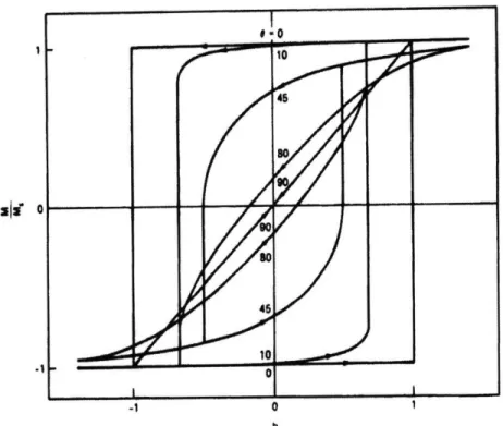
This single domain to muti-domain transition is due to the minimization the total energy which is related to the wall energy and magnetostatic energy. The wall energy is determined together by exchange energy and anisotropy energy [12-14]. The switching mechanism changes to domain wall motion for multi-domain structure. For single domain structure, the switching mechanism is coherent (spin rotation) for smaller particle size, but becomes incoherent (such as buckling, curling) [12-14]. When the single domain particle size is further reduced, the magnetic nanograins become superparamagnetic which will be further explained in the next section [13]. The working region of magnetic recording media is the shaded single domain, thermal stable region with particle/grain size between d, and do. In this range, the non-interacting single domain particles behave magnetically according to the series of hysteresis loop at different aligning angles 0 between easy axis and applied magnetic field shown in fig. 2-6, assuming coherent rotation (Stoner & Wohlfarth, 1948).
0 6. 30 0
U
ds doParticle diameter d
No
Fig. 2-5 [12]: Coercivity He vs. grain size d.
sIx
-1 0 1
h
Fig. 2-6: Series of hysteresis loop of a single domain particle with various aligned angles
2.3. Limitations of Conventional Media and Superparamagnetic Effect
The magnetic grain size is scaled down by tuning thin film processing parameters, consequently, size of one magnetic bit which consists of a certain number of magnetic grains is shrunk and thus more data can be stored per unit area. When the grain size is scaling down to a limit, the media is subject to superparamagnetic effect where the energy barrier required to change the direction of the magnetic moment of a particle is comparable to the ambient thermal energy. It is a small length-scale phenomenon by which magnetic materials exhibit a behavior similar to paramagnetism below the Curie or the N6el temperature. At this crossover point, the rate at which the particles randomly reverse magnitization direction becomes significant and thus the magnetic particles behave paramagnetically even at ambient temperature. The bit thus becomes unstable and data is lost. To calculate the smallest magnetic grain size that can be used for information storage, let us consider the rate of magnetization switching expressed by Arrhenius Neel law:
1
r = -exp(-E, I kBT), (Eq. 2.3)
where EB is the energy barrier with the existence of an external field of H,
fo
is a constant representing the attempt frequency on the order of 109-1012 Hz, k, is the Boltzmann constant, and T is the temperature.EB can be expressed as [1]:
H
E8(H,V) = K V(1l--) M , (Eq. 2.4)
where Ku (magnetic property of material) stands for uniaxial anisotropy constant, V is the volume of the magnetic grain, The exponent n is 1.5 in isotropic longitudinal media, and Ho is the intrinsic switching field which is related to the required write field H, by [8]:
K,
Ho a H, s Hý ; (Eq. 2.5)
M,
For data storage stable under zero external field for over 10 years (industry standard) at
ambient temperature, the criteria is calculated to be EB = KV > 40k,T . That means
thermal stability imposes a minimum bit size which can be reduced to. The minimum grain and thus bit size vary for different magnetic materials with different anisotropy constants. This theoretical estimation is based on assumptions of isolated particles and coherence switching mechanism [4]. However, the interactions among the magnetic grains in the conventional recording film must be considered as they are closed to each other separated by a distance of grain boundaries only. The energy barrier can be lower by exchange coupling between magnetic particles in thin film [6]. Also, as mentioned earlier, the media noise depends strongly on the microstructure of the film including the grain size distribution, grain orientation and also grain boundaries [6]. This implies better thermal stability of patterned media compared to conventional media with same bit size and thus less stringent on bit size limited by thermal stability criterion. In addition, incoherent switch mechanism gives an energy barrier lower than coherent switching as well. If the 10 years thermal stability criterion of KUV/kBT 2 60 for thin film media is used, assuming K, = 2.5 x 10⁶ erg/cc 2 [15] for Co-alloy [6], the minimum grain size is
calculated to be 9.7 nm. Range of magnetic grain size in modem magnetic recording is around 5-15 nm [7] which is already approaching the superparamagnetic limit of current magnetic recording materials Co-alloys.
People have considered to reduce the superparamagnetic limit size by using high anisotropy materials such as FePt or CoPt, but their large coercivity (K =6x10⁶ -10x106 erg/cc for bulk Llo FePt [16]) far exceed the writing field
capacities of modern write poles with saturation magnetization density approaching the highest recorded value (~26 kGauss3 [15]) [7] and that is how heat assisted magnetic
recording comes up (problems of this approach will be addressed later in the competing technologies section).
2 erg/cc: CGS unit which stands for energy per cubic centimeter, 1 erg = 107
J. 3 Gauss: CGS unit for magnetic flux density, 1 G = 10" T
2.4. Patterned Media and Technical Barriers for Its Implementation
To summarize, the triangular conflictions among thermal stability, SNR and writability restrict the areal density of conventional thin film magnetic media from further increasing.
Patterned media can solve the problem by making well ordered, uniform size, discrete magnetic islands which'are single magnetic particles, with each island storing one bit. In this way, we can reduce the bit size using writable magnetic materials with moderate anisotropy constant, providing good thermal stability and acceptable SNR [1].
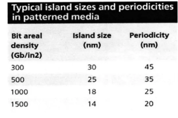
The schematic drawing in fig. 2-7 shows the nanoarrays we need to fabricate for patterned media. In order to achieve aimed areal density of 1Tb/in2, the nanodot dimension is around 12.5 nm which challenges the current nanoprocessing techniques [17]. Table 2-1 gives the island sizes and periodicities with regards to various bit areal density requirements.
/Nonmagnetic
Mannati
'
\
Tyia isadszsad eidcte
Bit areal island size Periodicity density (nm) (nrm) (Gblin2) 300 30 45 500 25 35 1000 18 25 Areal density = 1Tb/sq in 1500 14 20
Fig. 2-7: A schematic drawing showing Table 2-1: Theoretical island sizes and nanoarrays of patterned media and periodicities in patterned media with theoretical dimensions for 1Tb/inch2 areal regards to various areal density density (Courtesy: S.N. Piramanayagam). requirements (Hitachi).
For patterned media to be finally implemented in real production, the most challenging task is the media fabrication. Although the concept of discrete islands disk seems straightforward, there are many stringent requirements on the fabricated media. The first requirement of patterned media is to make nanoscale bit islands with dimensions less
than 25 nm to achieve superior density compared to the recent implemented perpendicular magnetic recording (PMR). An areal density of 345 Gb/inch2 has been demonstrated on PMR by Hitachi researchers in 2006. The highest areal density HDDs using PMR technology which is about 240 Gb/inch2 were shipped July, 2008 by Seagate.
It is estimated that to achieve higher areal density compared to the current perpendicular magnetic recording, the periodicity of the patterned nanoarrays should be less than 50
nm, which means that the island dimension should be less than 25 nm. At this dimension range, the magnetic particle is expected to be single domain [4]. The second requirement is the aspect ratio of the magnetic island can not be too high, in order to ensure coherent magnetization reversal. Coherent magnetization reversal is favored for high writing speed, because it has shorter sub-nanosecond switching time compared to incoherent switching which is around 1-2 ns. Besides nanoscale dimension, moderate aspect ratio, the nanoislands must have uniform size and shape and well ordered into nanoarrays with enough separation distance, which keeps the switching field distribution narrow and ensure good performance of the media. Last but not least, the bit sizes have to be controlled above superparamagnetic limit of the selected magnetic materials for thermally stable performance [4].
Besides the fabrication challenge with the highest technical barrier, other essential elements for patterned media commercialization include: 1) read sensor revolution which can read nanoscale bit, 2) flyabiltiy which allow the head to fly under 7-10 nm, 3) signal processing/synchronization. Technical barrier and these technologies are expected to be much lower compared to fabrication challenge although signal processing, in particular, synchronization is still at the research stage [1]. Read/write head is always under intensive research to accommodate higher storage density. Hitachi has announced the successful development of current perpendicular-to-plane giantmagneto-resistive (CCP-GMR) heads recently (Oct, 2007), which is expected to be implemented in shipping product in 2009 [18]. CCP-GMR is the smallest read-head technology currently (30-50 nm) developed for ultra-high-density storage media, and may be used in the patterned media HDD system [18]. Discrete track PMR media, which has recording tracks separated by grooves is under vigorous research, can serve as an intermediate technology
towards discrete bits media (patterned media). It has been shown experimentally that discrete track recording (DTR) media give noticeably better SNR and significantly lower adjacent track erasure compared with continuous media at the same track width, which are important when increasing areal density [19]. Flyability issue was also largely solved in developing discrete track media [17]. Therefore, whether and when patterned media can be realized mostly depend on the fabrication methods development and innovation, which will be addressed later after the discussion of competing technologies.
3. Competing Technologies of Patterned Media
3.1. Heat Assisted Magnetic Recording
The most possible internal competing technology of patterned media is heat assisted magnetic recording (HAMR). Basically, this technique uses a laser to locally heat the magnetic material during writing process to lower down the coercivity of the materials below the available write field [20]. Therefore, as discussed, materials with a higher anisotropy can be used so that the grain size limited by the superparamagnetic effect can be further reduced and thus areal density is increased. Seagate CTO Mark H. Kryder predicted that with this technique, a thermally stable grain size smaller than 3 nm can be achieved by using high anisotropy media such as Llo FePt, which gives areal densities well beyond 1 Tb/in2theoretically [21].
Although the principle and fabrication of HAMR seems easy, it's not yet commercialized yet as it is facing a lot of technical challenge. The major problem comes from the high working temperature and thermally induced mechanical failure. Both the air pressure change at the laser spotted area and the nano-deformation of the slider body will lead to noticeable change of slider's flying performance. Repeated heating and cooling process can also lead the head-disk interface to intense thermal strain/stress fields. Furthermore, the stress field can change the magnetization behavior of the grains thereby affecting the magnetic performance such as the permeability in the head [22, 23]. Also, integration of optical elements (laser) with magnetic elements in one head is challenging. The optical spot size has to be small enough to give the localization of medium heating which should be no larger than the order of the recorded bit size [24]. Last but not least, since high Ku materials have a chemically ordered structure that requires elevated substrate deposition temperature, fabricating reduced grain sizes is much more of a challenge compared to current Co-alloys [20].
As we can see, there still remain many challenges for HAMR to be realized. It is difficult to predict whether HAMR or patterned media will come out first. Although there is possibility that HAMR comes before patterned media, it will not affect the development of patterned media which could be built upon HAMR technology and further extend the areal density. Therefore, Rather than saying HAMR is a competing technology of patterned media, it is more like a stepping stone that will give the disk drive industry breathing room to explore and develop ultimate ultra-high-density recording technology such as patterned media.
3.2. Flash/Solid State Drive
Solid-state nonvolatile memory market has grown at an incredible rate since first introduced around fifty years ago. Floating gate (FG) device is the dominate design in this industry from the beginning till today. The floating gate flash cell is structurally different from a standard MOSFET in its floating gate, which is a polysilicon layer electrically isolated by dielectrics The most widespread memory array organization is the so-called flash memory, which got its name because it could not be erased by bytes but
could only be erased by the entire chip or large sections of the chip [25]. The first commercial flash product was invented in Toshiba in 1984 [26]. It has been quickly expanding its market because of much lower cost than byte-programmable EEPROM (Electrically Erasable Programmable Read-Only Memory) and therefore has become the dominant technology in non-volatile, solid-state storage industry. Although a huge commercial success, the floating gate flash is approaching its limit for continuous scaling of the device structure beyond the 65 nm node. This scaling limitation stems from the extreme requirements put on the FG isolation layers, in particular the tunnel oxide isolating the FG layer from the crystalline silicon substrate. Tunnel-oxide thickness with values in the range of 9-11 nm can be hardly further reduced in recent flash memory developing, implying a scaling rate that is not comparable with that of transistors [27]. A novel technology - embedded nanocrystals (NCs) flash technology, coming as a solution for flash device scaling problem, is under intensive research [28, 29] and is expected to be commercialized in 2009. This technology provides the flash devices better endurance characteristics, longer retention time and fast read/write [30].
However, further scaling down of flash cells still faces challenges which keeps their areal density lagging behind HDD, and their price per bit is not comparable to HDD (refer to appendix 2 for comparisons). Although solid state drive/flash is attractive when considering speed, noise, power consumption, and reliability (refer to appendix 2), it is expect that as long as hard disk drives can continue the areal density growth rate, they will enable capabilities and features that are not possible at an attractive price with SSD.
4. Fabrication Methods for Patterned Media
4.1. Lithography Patterned Media
When fabricating uniform nanoarrays with well-defined position and size, lithography patterning is the first nanoprocessing technology that researchers think about. The discrete island of patterned media should be patterned based upon the perpendicular recording media [1]. The material used today for the magnetic film in current magnetic recording technology is CoCrPt polycrystalline alloy with some addition components such as B or Ta. During the annealing process, the added elements improve the
compositional segregation into magnetic grains which is high in Co and surrounding nonmagnetic region which is low in Co [6]. The magnetic grains has their easy axes perpendicular to the disk plane in perpendicular recording media, while are parallel to the disk plane in longitudinal recording media. PMR is preferred as a base point for the fabrication of patterned media because it provides better writability (write field = 4irM,, [7] twice larger than longitudinal recording), better orientation uniformity, extended higher areal density and was well established recently.
4.1.1. Conventional lithography techniques
Refer to table 4-1 for a summary of the conventional lithography techniques. These techniques are said to be conventional because they are all top-down approaches for fabricating nanostructures. Some of them are high resolution techniques which were developed and commercialized in recent years such as E-beam lithography and nanoimprint lithography.
From the discussion of the patterned media requirements, well ordered nanoarrays with periodicity less than 50 nm need to be fabricated for patterned media, which implies a minimum resolution of 25 nm. By examining the resolution limit of each listed lithography method, it can be found that only EUV, X-ray, E-beam lithography, focused ion beam lithography and nanoimprint lithography can satisfy the resolution requirement. However, EUV lithography and X-ray lithography are extremely expensive because of the requirement of complex optical system, stringent requirements of the masks. For an areal density of ITb/in2, even higher resolution (-12 nm) is needed which challenges the
state-of-art high resolution lithography techniques. Focused ion beam lithography is more expensive compared to E-beam. Therefore, only E-beam lithography and nanoimprint lithography will be discussed here.
R = kLNA X - 10-14 nm, R - 30 nm ?,- 0.2-10 nm, R - 20 nm R = /?2sinO R -- 10 nm R - 10 nm R ~ 5 nm demonstrated (Fig. 4-3) [31]
Table 4-1: A summary of conventional lithography resolution limits and other limitation [32, 33].
Low resolution, state-of-art: R - 60 nm
Strongly absorbed by almost all the materials, special mask needed Besides the same problems above, high intensity x-ray source needed Difficult to obtain circular pattern
Low throughput, high cost,
proximity effect4
Low throughput, high cost Resolution relies on stamp fabricated by other methods such as E-beam, high cost of stamp, stamp wear and lifetime
methods with comparisons of
Let us look into scanning electron beam lithography (SEBL) first. SEBL can write patterns of almost all arbitrary shape with high resolution (-10 nm) by scanning the electron beam through the resist surface with no need of mask. The patterns are divided into pixels and defined using computer-aided design (CAD). The pixel size is determined
by the size of the electron beam, and it takes longer time to write larger pattern areas with
more pixels. A beam blanker is used for stop the electron beam from reaching the resist area without pattern. Large area of pattern is divided into many fields within which the electron beam is defected to the exposure pixel and stage movements are not needed (fig. 4-1) [33]. Refer to table I in appendix 3 for various actual field dimensions corresponding to different combinations of pixel size and digital field size.
4 Proximity effect in E-beam lithography: during an e-beam exposure of the resist, the interaction
region with electrons is larger than the size of the incident probe due to elastic and inelastic scattering of the electrons in the resist and substrate materials. Distortion or blurring of the transferred pattern happens from this effect.
Conventional optical lithography Extreme ultraviolet lithography
X-ray lithography
Interference lithography
Electron beam lithography
Focused ion beam lithography
Nanoimprint lithography
.... . .
~---Fabriction mthodsResoluion ()
Limiation
I IB
A field
Fig. 4-1: A schematic drawing showing the concept of pixel and field.
The total scanning time is limited by: (1) resist sensitivity; (2) beam current; (3) data rate limits on the tool; (4) stage motion; and (5) shot noise limitations on resolution [34]. Refer to table II in appendix 3 for exposure time/pixel transfer rate with respect to resist sensitivity and current density, and typical data rates for different SEBL types are shown
in table III.
The beam spot size can be calculated using expression:
d
= (4i/K2B)/2 a, (Eq. 2.6)where numerical aperture/half angle a 10-3, i is the beam current related to brightness (B), which varies for different electron sources. The beam current density is related to the
source brightness by:
J = rcBa 2 (Eq. 2.7)
The exposure time per pixel or the dwell time per pixel is:
t, = S / J, (Eq. 2.8)
where S is the resist sensitivity in C/cm2 (or e-/nm2/pisec).
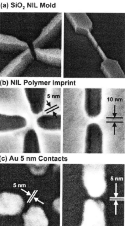
The second high resolution lithography technique to be discussed here is nanoimprint (refer to fig. 4-3 for 5 nm feature size demonstrated). There are mainly two groups of nanoimprint lithography (fig. 4-2): a) thermal nanoimprint. In a standard T-NIL process, a thin layer of imprint resist is spin coated onto the sample substrate. Then the mold,
which has predefined topological patterns, is pressed into the resist under certain pressure and at elevated temperature which is above the glass transition temperature of the resist polymer. After being cooled down, the mold is separated from the sample and leave resist pattern on the substrate. Finally, a pattern transfer process such as reactive ion etching transfer the pattern in the resist to the underneath substrate. b) UV
nanoimprint/step-and-flash lithography. In UV-NIL, Photo curable (UV sensitive) low viscosity resist is applied to the sample substrate. Then the mold made of transparent material such as fused silica is brought into contact with the resist, which is cured in UV light meanwhile and solidifies. After mold separation, a similar pattern transfer process is used to transfer the pattern in resist onto the underneath substrate [35].
a) b)
j .9
(a) SiO, NIL Mold
(b) NIL Poilymer imprint
(b) NILPolymerImrn
h.- Ai R nm (nntnrtr.
Fig. 4-3: The 5 nm feature fabricated using UV-NIL.
4.1.2. Templated self-assembly of diblock copolymer lithography
After the invention of nanoimprint lithography by Stephen Chou in 1995 [37], people proposed to use this cheap and high resolution technique to enable the mass production of patterned media [4, 17, 35, 36, 38]. However, a master stamp/mold with large area of nanoarrays still needs to be fabricated using other high resolution lithography method such as E-beam lithography. The time and price of making such a stamp using E-beam is enormous and not practical, which scares HDD manufacturers to pursue it (cost estimation will be provided later). A cheaper way to fabricate the stamps is using templated self-assembly of diblock copolymers.
Self-assembly of diblock copolymer has been demonstrated as a promising template for nanoscale lithography since 90th. Diblock copolymers A-B consist of two chemically different polymer chains or blocks A and B joint together. Because of connectivity constraints and the incompatibility between the two blocks, if A and B do not mix, the copolymer film spontaneously self-assemble into ordered point-like or linear patterns over a large area of alternating chemical composition at equilibrium [39]. General
processing steps are firstly depositing a thin polymer spin-coating of films using polymer solutions in toluene onto the desired substrate and the film thickness is controlled by varying spinning speed and polymer concentration. The films were annealed around range 1000C-2000C which is a temperature above glass transition temperatures of the polymers, for significant long time to obtain well-ordered morphologies. Upon annealing, block copolymers self-assemble into nanometer scale domains to minimize the free energy of the whole system [40, 41]. Either block could then be selectively removed due to their chemical or physical properties dissimilarities, leaving nanostructures of the other block which can be used as mask for lithography. The microdomain patterns are transferred directly to the underlying substrate [42].
The morphology of the phase largely depends on the volume fraction of the blocks at a given XN [43]. Spherical morphology is patterned media applications. The domain period depends on the segment length of the polymer, the overall number of segments, and the Florey-Huggins interaction parameter for a certain block copolymer [39]:
<< 1, disordered, unperturbed chains
Nj - 10, weak segregation, fluctuations aN"/ 2 (Eq. 2.9)
>> 10, strong segregation, D ~ aN2/3 1/ 6
where ' is the Florey-Huggins interaction parameter, N is the overall number of
segments/monomers, and a is the segment length. From this theory, in order to get islands-sea microstructure with minimized nanoscale domain size for patterned media, it is not only necessary to control the volume fraction of each block, but also very important to choose the diblock copolymer with high X. In addition, the polymers should have good etching selectivity between the two blocks to make lithography process feasible. It is possible in theory for diblock copolymers to self-assemble into ordered periodic structures at the molecular scale (5 to 50 nm) [44], however, the smallest domain size demonstrated in experiment is 18 nm which has not met the requirement for 1Tb/in2 areal density.
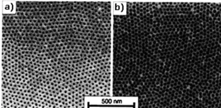
Dense periodic nano-arrays of holes and dots with feature size down to 20 nm have been fabricated on a silicon nitride coated silicon wafer using asymmetric polystyrene-polybutadiene (PS-PB) and PS-polyisoprene (PI) diblock copolymers [42] (see fig. 4-4).
Fig. 4-4: a) SEM micrograph of a partially etched, ozonated monolayer film of spherical microdomains. PI domains were exposed as holes which appear darker after the continuous PS matrix at top was taken off; b) SEM micrograph of hexagonally ordered arrays of holes in silicon nitride on a thick silicon wafer. The pattern was transferred from a copolymer film such as that in a).
However, diblock copolymer as a self assembly system suffers common problems of self-assembly such as defects and lack of long-range order. Topographically [45]/chemically [46] patterned substrate can be used to template/guide the self-assembly of diblock copolymer for fabrication of defect-free nanostructures with long-range order. Paul Nealey's group from Wisconsin Research proposed chemically patterned imaging layer on the substrate formed by interference patterns of two or more extreme ultraviolet EUV beams. The patterned surface manipulates the wetting behavior of diblock copolymer films and guides the spatial microphase separation of PS-polymethylmethacrylate (PMMA) in their experiment, which transfers the imaging layer pattern to polymer film [46, 47]. However, the feature and domain size formed by this technique depends on the imaging layer patterned by other lithography method. It seems not really manifesting the good features of diblock copolymer self-assembly lithography such as high resolution and low cost. Another approach is to use topographical templates such as trenches or shallow grooves. J. Y. Cheng and C.A. Ross et al from MIT have experimentally and theoretically (free energy minimization) designed topographical templates (grooves)
which can lead to precisely modulated diblock-copolymer nanostructures with controllable spatial arrangement of sphere arrays [48, 49]. By combining top-down and bottom-up nanofabrication, templated self-assembly of PS-polyferrocenyldimethylsilane (PFS) block copolymer gave perfect, close-packed arrays of PFS spheres with long range order in PS matrix. Very few defects were observed up to 12 rows with a long range
order of at least 20acros long (acro,,,,, is the centre-to-centre spacing shown in fig. 4-5 a,
right, which is 28.6 nm for this polymer). A preferential wetting brush layer of PFS molecules (see fig. 4-5 a, left) were found both at the bottom and sidewall of the silica grooves, which has a thickness t ~10 nm. It was assumed that the preferential wetting layer on the vertical sidewalls of the groove drives the domain ordering [50].
The key in this technique is to ensure the width of the groove to be commensurate with the ideal periods for desired number of sphere rows, which were determined in their experiment (see fig. 4-5 b and c) [49]. When the groove width is incommensurate with the ideal period, the resulting block copolymer domains have defects and are compressed
or expanded to fit the groove. Near-perfect arrays of N rows of islands formed for a
confinement width W where (N - 0.5)d < W < (N + 0.5)d. Confinement width is the
actual groove width minus the thickness of two brush layers on the wall, and d is the equilibrium row width and is 24.8 nm for this polymer (see fig. 4-5 a, right) [49, 50]. For example, in order to fit N = 9 rows of stable spherical domains, the confinement width is
8.5-9.5d. And the actual groove width can be calculated to be Dgroove = Wd + 2t = 230.8-255.6 nm.
a) b) 13 i 12- 11-C) -10 1 1 2 is Confinement width (d)
Fig. 4-5: a) schematic drawings of spherical PFS domains in PS matrix and equlibruim row width d; b) Plan-view scanning electron micrograph of ordered arrays of PFS domains with N = 2 to 12 rows; c) The number of rows in the groove, N, plotted against confinement width, W, showing the widths at which arrays with N rows are stable. The confinement width is expressed in terms of d, the equilibrium row spacing, which is 24.8 nm in this polymer.
Similar studies were also done by K. Naito et al. in Toshiba research team using PS-PMMA. A paper reporting their demonstration of a 2.5 inch disk with patterned nanoarrays (fig. 4-6) was published [38]. However, the island size formed is around 40 nm which is too large for patterned media application. Also, their study did not show a precise control of the groove width over number of nanoarrays rows. It seems that they
I:: ::::I·
:
000
94Ode
*d*
have little control over the domain size and groove width for precisely modulated diblock copolymer nanostructures. Nevertheless, it is the first patterned media prototype fabricated by topographically templated self-assembly of diblock copolymer, which shows the feasibility of this technology for patterned media application. Patents were granted on their work [51-53].
Co74Cr6Pt, dot
Fig. 4-6: Demonstration of 2.5 inch disk with patterned nanoarrays by K. Naito et al.
4.2. Self-Assembled Nanomagnets Patterned Media/Nanocrystal Superlattice
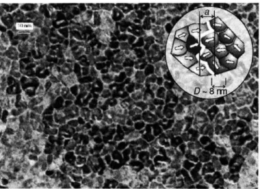
Nanocrystal (NC) superlattices have attracted increasing attention since they were first reported in 1989 [54]. The general approach is to firstly chemically synthesize the nanoparticles, and then spread the colloids on the substrate and let the carrier solvent to evaporate slowly followed by annealing [55]. Self-assembled FePt nanocrystal superlattice was reported by IBM Research Centers and Seagate Research together in 2000 [55]. Synthesis of monodisperse iron-platinum (FePt) nanoparticles by reduction of platinum acetylacetonate and decomposition of iron pentacarbonyl in the presence of oleic acid and oleyl amine stabilizers produces particle sizes available from 3 to 10 nm (diameter). The synthesized particles also have narrow size distribution with a standard deviation of less than 5%. However, these nanoparticles are not suitable for patterned media as they are paramagnetic. Thermal annealing converts the internal particle structure from a chemically disordered FCC phase to the chemically ordered face-centered tetragonal phase, which transforms the nanoparticle superlattices into ferromagnetic assemblies. However, annealing process reduces the inter-particle spacings from -4 nm to -2 nm which is too close for patterned media application (refer to fig. 4-7 below for the superlattice structure). It was claimed that the separation distance may be increased by capping ligands on the nanoparticles [55]. Later experimental and
theoretical study shows that low temperature (<5500C) annealed FePt assembly can contain a significant fraction of superparamagnetic particles, while higher temperature annealing (>6000
C) lead to significant aggregation of the FePt nanoparticles with the presence of undesirable ferromagnetic coupling between particles [56]. The results imply that it is very difficult to control the annealing temperature for forming desired L lo0 phase of FePt without significant nanoparticle aggregation. Although this is not yet a mature technology for fabricating patterned media, Seagate was granted a patent on self-assembly of nanoparticles such as FePt in locking patterns defined by conventional lithography method, which has similar concept as templated self-assembly of diblock copolymer discussed above [57] (see appendix 8). After this study, some researchers coated the FePt particles with coatings like SiO2 (or Fe304 [58]) to improve the chemical ordering of FePt nanoparticles, and achieved FePt NCs superlattices with coercivity as large as 18.5 kOe5
[15] in spite small size of 6.5 nm [59]. This implies that it can be used to increase the areal density; however, this is still conventional media technology, which is not economic as the increasing in areal density may not be able to compensate the cost.
Fig. 4-7: TEM micrograph of a 3D assembly of 6 nm FePt sample made by Shouheng Sun et al.
Another significant work is the self-assembled cobalt nanocrystal supperlattices over a lithographically patterned area (-100 nm by 100 nm) demonstrated by C. T. Black and Shouheng Sun et al [60]. They also obtained a patent on magnetic storage medium formed of self-assembled magnetic particles [61].
5. Comparisons of Technologies and Possible Fabrication Schemes
First of all, let us recall back previously discussed nanoprocessing techniques which are potential for patterned media fabrication: 1) scanning electron beam lithography (SEBL);
2) nanoimprint lithography (NIL); 3) topographically templated self-assembly of diblock copolymer; 4) self-assembly of magnetic nanocrystals.
5.1. Technique 1) and 2)
Among these techniques, the first two (SEBL and NIL) are top-down methods which are mature and commercialized technologies, with companies providing lithography
facilities, materials, masks and services. The nanoimprint lithography business emerged in the late 1990s, started with Nanonex and Obducat. EV Group, Molecular Imprints and Suss also announced tools subsequently. Molecular have recently released one new system to Hitachi -"IMPRIO HD 2200" especially for development of patterned media. Toshiba also says it has shipped a few systems from it, mostly in Japan [62, 63]. Today's leading-edge 193 nm immersion optical scanners (- 60 nm feature size) sell for as high as $40 M. In contrast, a state-of-the-art nanoimprint tool may sell for up to $10 M, and most nanoimprint tools sell for as cheap as $100,000 [62, 63]. By comparison, the price of SEBL facilities is generally above $4 M [64]. However, nanoimprint needs master stamp generated by other high resolution lithography method, which can be quite expensive too.
5.2. Technical Barriers of 3) and 4) for Patterned Media Fabrication
The latter two techniques involving self-assembly (bottom-up) are still in research stage. And in order to achieve long-range order for patterned media application, self-assembly is usually combined with top-down methods, which provides topographical template for self-assembly processes. The structures made by technique 3) showed in the experiment give defect-free long-range order area of around 300 nm by 400 nm [49]. However, for patterned media, we need to make defect-free nanostructures of even longer-range order
(- cm). Cheap and convenient characterization methods are needed for examination of
defects; signal processing techniques need to be developed for error detection and correction to accommodate for the defects if there are. Technique 4) which is self-assembly of magnetic particles not only has the same problems as 3), but also, FePt nanoparticles with very small dimension (3-10 nm) are not ferromagnetic without annealing while the NCs tends to aggregate after annealing. Also, the separation distance between NCs is too small for patterned media. Therefore, both 3) and 4) technologies
have problems and are not ready for patterned media. However, the last one which evolves more complex chemistry has relatively high technical barrier currently, thus more studies need to be done to further prove its feasibility as a fabrication method for patterned media. In contrast, the diblock copolymer self-assembly system has been proved in a patterned media prototype [38]. It is also more flexible which can adjust to a range of groove width commensurably, compared to magnetic hard particles (colloid) self-assembly in which defect-free ordering only occurs for certain widths [49].
In the case of guided self-assembly of diblock copolymer, we do not need to write the bit one by one, islands will form by self-assembly. However, circular grooves are needed to facilitate the ordering, otherwise, the self-assembled nanoarrays lack long range order (a necessary requirement of patterned media). As templates such as grooves are needed to guide the self-assembly process, the area available to pattern the nanoarrays is reduced and therefore smaller bit dimension is needed to achieve the desired areal density compared to whole surface patterning. According to studies mentioned by K. Naito et al, their groove widths varies from 60 nm to 250 nm, and the land spacing between grooves was kept as 400 nm [38]. A schematic drawing below (not to scale) shows the grooves needed to guide self-assembly of diblock copolymer within them. The Ni master disk stamp with these circular groove patterns were purchased from Nikon Corporation (price unknown) [38] and in the experiment of Ross et al, they used E-beam to draw the groove patterns [49].
Groove width: 60-250 nm
Spacing: 400 nm
Fig. 5-1: A schematic drawing which shows the grooves and spacing dimensions formed by the Ni master stamp in the experiment by K. Naito et al.
The data density is thus only a fraction of the potential density with nanoarrays on the
whole surface. This fraction can be estimated as
f
= groove , where Dgroove isD groove +Dspacing
the width of the grooves and Dspacing is the width of inter-groove spacings. Let us use the
experiment results of Ross et al. as an illustration to calculate the areal density generated by this technique. W rows of polymer nanoarrays are formed in the groove with row spacing of d and inter-particle spacing of across. The areal density in the patterned area can be calculated as:
x 101 x 2.542 (bits / in2 )
across X Ogroove
The whole disk areal density can be estimated by:
Areal density of patterned area x f ( f = groove
Dgroove + spacing
W
x (Wdx+2) 1014 x 2.542(bits/in2) 2d x (Wd + 2t) Wd +2t +Dspcing 2= W + 2 D-) x 1014 x 2.542 (bits /inch2) 2 dWd+2t+Dspacinga,- =
111 1 d --2 "?
o =24.8 nMIFig. 5-2 [49]: Schematic drawing showing the row spacing d and particle spacing across.
Where d is the equilibrium row spacing, W is the number of rows, t is the thickness of polymer brush layer. Substitute the actual experimental values of d = 24.8 nm, W=12 (maximum), t = 10 nm [49] into the formula, and let Dspacing =100 nm, we get total areal
density of648Gb/in2. Therefore for this technology to be applied for patterned media fabrication to achieve 1Tb/in2 areal density, more research is needed to further reduce the
periodicity or domain size of the diblock copolymer self-assembly systems. The size of
the spherical nanodomains depends largely on the length of the blocks and the Florey-Huggins interaction parameterX as discussed in earlier section. More R& D work needed to achieve smaller domain size and longer-range order (- cm) in which we could contribute and generate value.
5.3. Possible Patterned Media Fabrication Schemes
Technically speaking, possible fabrication schemes of patterned media are: A) SEBL+NIL; B) topographically templated self-assembly of diblock copolymer + NIL; C) self-assembly of magnetic nanocrystals. A schematic drawing below shows the current technological barriers for the three fabrication scheme with respect to technology evolution timeline. Scheme A) has the lowest technological barrier because both SEBL and NIL are relatively mature and commercialized technologies. The only problem is that the resolution of current SEBL can only reach 10 nm generally, and proximity effects also affect the quality of dense features like which in patterned media. Scheme C) has the highest technological barrier while scheme B) has medium barrier compared with the other two. The reasons were stated above when discussing the technological barriers of templated diblock copolymer self-assembly and NCs superlattice respectively.
Technological Barriers
Fig. 5-3: Comparisons of the technological barriers among fabrication schemes A), B)
PART II: COST, IP & BUSINESS MODEL
6. Cost Estimations and Comparisons for Fabrication Schemes 6.1. Comparison of Cost: Scheme B) vs. Scheme A)
- Templated Diblock Copolymer Self-Assembly vs. SEBL
Using self-assembly of diblock copolymer guided by circular groove to fabricate the stamp is a relatively cheaper method compared with E-beam lithography. After the stamp is made, the following cost in the next step is not significant compared to the stamp cost because mass production is enabled by using nanoimprint lithography. Also, you can use the father stamp to make many daughter stamps using nanoimprinting.
Below is an approximated calculation to show how much usage of E-beam lithography equipment costs to write a 2.5 inch disk area with island dimension of 10 nm which gives an areal density of 1.5 Tb/ inch2.
Let us consider the data rate and the stage moving/settling time as the limiting factors for total scanning time. By approximating the stage moving/settling time to be 4 sec from field to field [34] and assuming 10 nm pixel size (one pixel for one magnetic island), the total writing time for JBX-9300FS EBL System (microelectronic research center, Georgia Tech) (50 MHz) to pattern a whole 2.5 inch (6.35 cm) disk surface with 14 bit
(164 pm) field (table I, appendix 3) can be estimated:
t,ota,= ntdata + Ntsettle,, = (n
-
2x 10-'
+N N. 4)sec6.35cm)2
N= Ato - 2 31.7cm 1.2 x 10⁵
Afield (1642pm)2 2.7 x 10⁻⁴ cm 2
x0.65mm)
n=N( 20nm =109N
To estimate the E-beam equipment usage cost per hour, we use JBX-9300FS EBL System (microelectronic research center, Georgia Tech) as an illustration. The equipment specifications and its usage cost can be found in appendix 4. It is estimated to be $1600/hr for industrial usage.
Cost of E-beam equipment usage for pattering a 2.5 disk with 10 nm island size is thus: 800hrs x $1600 / hr = 1.28millon
Plus all the cost, the total cost per one stamp easily exceeds 1 million. Comparing this value with the total revenue 32.8 billion of the whole HDD industry for year 2007, it can be concluded that the cost of the stamp is significant.
As calculated based on experimental results, we get total areal density of 648Gb/in2 by
templated self-assembly of diblock copolymer with inter-groove spacing widths of 100 nm. If we can form smaller domain sizes (imply smaller d), the areal density can be further increased till comparable with that made by E-beam lithography. While the cost of this technique is about 50 times lower than E-beam. To estimate the cost of a stamp made by templated self-assembly of diblock copolymer, we need to know the cost of the master stamp with spiral patterns. The price of this master with feature size down to 100 nm can be estimated to be around $16,000 according to nanoimprint vendors [65]. Because the materials cost of polymers is not significant (- $300) compared to spiral patterned master cost, and plus the furnace cost (-$1000), spin coating machine (-$2000) cost, the total cost will be around $20,000.
6.2. Comparison of Cost: Scheme B) vs. Scheme C)
- Diblock Copolymer vs. Magnetic Nanoparticles
Both technologies use the same concept to achieve well-ordered nanoarrays. Both need templates/locking patterns to guide the natural self-assembly processes. The difference is that by scheme c), the magnetic islands assemble in one single step with no nanoimprint lithography process followed. Self-assembly of diblock copolymer, however, is just used to fabricate the stamp which is then used to nanoimprint the resist on disk substrate and
finally the pattern is transfer to the magnetic layer by etching, leaving magnetic nanoarrays. This does not mean that NCs supperlattice is cheaper, because the same set of nanoimprint lithography steps is still necessary to imprint the groove patterns per one disk. That means that these two technologies would incur almost the same cost per disk assuming that no big difference in the materials cost (provided cheap and large amount supply of NCs). And the throughput may be lower which is limited by the self-assembly time of NCs.
6.3. Proposed Fabrication Scheme: Scheme B)
Table 6-1 gives a summary of comparison between technologies for making patterned media discussed above from aspects including cost, throughput, technical barrier and overall commercialization potential. We can see that scheme B) has medium technical barrier and is the most promising one for mass fabrication of patterned media when cost per bit comes into consideration.
1 c•, v-lu. Ivllv at U3 ~ vi Lo"ACcullliUSIU~1 patterea meala Iaoricatlon.
The general fabrication process would be (refer to fig. 6-1): 1) lithographically pattern the concentric circular grooves on a mold substrate (can purchase from vendors); 2) let the
diblock copolymer to self-assembly in the groove, forming islands-in-sea nanostructure; 3) selectively etch away one polymer and transfer the pattern to the stamp substrate; 4) use the stamper to nanoimprint the patterns onto the PMR disk.
-• --. ,, (ion milling)
e4:--mstering by
LBR I EBR
stamper
nann Imnrlntinn
self-assembling
Fig. 6-1: A schematic drawing [17] of patterned media fabrication scheme B), the spiral patterns on the master stamp can be generated by other lithography methods or purchased from vendors.
Fig. 6-2: Dots with a diameter of 17 nm imprinted by Obducat's nanoimprint tools [66]. One problem with templated self-assembly of diblock copolymer as mentioned
previously is that you can not have nanodots on the whole disk surface, which means that the spacing land between grooves is a waste. In order to achieve the same areal density as whole disk patterning, the island dimension should be reduced by a factor of 1/f. And largefapproaching 1 is preferred for higher density. However, large f means spacing size
![Fig. 2-3: Schematic drawings showing the difference of write heads between longitudinal recording and perpendicular recording [8].](https://thumb-eu.123doks.com/thumbv2/123doknet/14756024.582559/8.918.457.776.151.334/schematic-drawings-showing-difference-longitudinal-recording-perpendicular-recording.webp)
![Fig. 3-1: Principle of HAMR [20].](https://thumb-eu.123doks.com/thumbv2/123doknet/14756024.582559/16.918.168.545.742.1045/fig-principle-hamr.webp)
![Table 4-1: A summary of conventional lithography resolution limits and other limitation [32, 33].](https://thumb-eu.123doks.com/thumbv2/123doknet/14756024.582559/20.918.134.797.142.568/table-summary-conventional-lithography-resolution-limits-limitation.webp)
![Fig. 4-2: a) thermal nanoimprint; and b) step-and-flash nanoimprint processes [36].](https://thumb-eu.123doks.com/thumbv2/123doknet/14756024.582559/22.918.147.771.490.891/fig-thermal-nanoimprint-b-step-flash-nanoimprint-processes.webp)