Allocating decoupling capacitors to reduce simultaneous switching
noise on chips
by
Adam Granich Unikowsky
Suibmitted to the Department of Electrical Engineering and Computer Science in partial fulfillment of the requirements for the degrees of
Master of Engineering in Electrical Engineering and Computer Science and
Bachelor of Science in Electrical Engineering and Computer Science at the
MASSACHUSETTS INSTITUTE OF TECHNOLOGY
June 2004@ Adam Granich Unikowsky, MMIV. All rights reserved.
The author hereby grants to MIT permission to reproduce and distribute publicly paper and electronic copies of this thesis document in whole or in part, and to grant others the
right to do so.
Signature of Author ....
-nim Granich Unikowsky
Department of Electrical Engineering and Computer Science May 20, 2004
Certified by.
Paul Stabler VI-A Company Thesis Supervisor
C ertified by ....
Christopher J. Terman Senior Lecturer, Electrical Engineering and Computer Science M.I.T. Thesis Supervisor
Accepted by . . . ...
Arthur C. Smith Chairman, Department Committee on Graduate Theses
MASSACHUSETS IN4SiTUE, OF TECHNOLOGY
Document Services
Room 14-0551 77 Massachusetts Avenue Cambridge, MA 02139 Ph: 617.253.2800 Email: [email protected] http://libraries.mit.edu/docsDISCLAIMER OF QUALITY
Due to the condition of the original material, there are unavoidable
flaws in this reproduction. We have made every effort possible to
provide you with the best copy available. If you are dissatisfied with
this product and find it unusable, please contact Document Services as
soon as possible.
Thank you.
Some pages in the original document contain text that
runs off the edge of the page.
Using decoupling capacitors to combat simultaneous switching noise in circuits
by
Adam Granich Unikowsky
Submitted to the Department of Electrical Engineering and Computer Science on May 20, 2004, in partial fulfillment of the
requirements for the degrees of
Master of Engineering in Electrical Engineering and Computer Science and
Bachelor of Science in Electrical Engineering and Computer Science
Abstract
Li noise due to simultaneous switching of circuits on chips is a growing problem in VLSI design. This kind of noise can lead to timing errors and significant circuit slowdowns, if not kept within reasonable bounds. The most common way of reducing this form of noise is the addition of decoupling capacitance on chip. However, adding decoupling capacitance can take significant area and can make routing very difficult. The goals of this thesis are twofold: first, to characterize the relationship between noise propagation on chip and parameters such as on-chip resistance and capacitance; and second, to develop an algorithm which will minimize the number of decoupling capacitors on chip while simultaneously reducing the noise to within acceptable boundaries.
Thesis Supervisor: Christopher J. Terman
Acknowledgments
I would first like to thank IBM Microelectronics as a whole for their support of my thesis. They provided
extremely generous financial support for all three years I worked at IBM, and provided me with easy access to any resource I ever needed. Numerous engineers took their time to answer my questions and provide with guidance about my summer internships and my thesis. Working at IBM was a truly outstanding experience
and I am truly appreciative.
I would like to specifically thank two people at IBM. First, this thesis would not have been possible without Tim Budell, my thesis supervisor at IBM. He spent countless hours teaching me, guiding me, reading my often impenetrable drafts, and putting up with my frequent silly questions. Without his support, this thesis would have been a pipe dream; with his support, it became a reality. I am indebted to him for his advice and his guidance.
I would also like to thank Paul Stabler. Paul was my manager at IBM for all three summers, during
which I had the opportunity to learn a tremendous amount about engineering and feel truly integrated into the IBM community. He provided invaluable support in choosing a thesis topic and a supervisor, and was a watchful eye throughout the thesis process. He always welcomed my questions and constantly gave me advice and guidance.
I was extremely privileged to have Professor Christopher Terman as both my undergraduate advisor and
my thesis advisor at MIT. For the past four years, Professor Terman has been a constant source of support as I navigated the waters of Course VI. As an undergraduate, his office doors were always open to me for any advice I ever wanted. As a graduate student, he provided with invaluable advice and direction as I struggled through the thesis process. I cannot thank him enough for his support.
Finally, I would like to thank my mother, father, and sister, for their unending love and support. They have been a rock of stability in my life and have helped me throughout my MIT career in ways unimaginable. It is to them that I am proud to dedicate this thesis.
Contents
1 Introduction 8
2 Methodology 10
2.1 The power grid . . . . 10
2.2 Current source methodology . . . . 12
3 Mathematical discussion 20 3.1 Effect of increasing current . . . . 22
3.2 Effect of decap on magnitude of peak noise . . . . 23
3.3 Effect of decap on time of peak noise . . . . 23
3.3.1 Application to determination of peak noise . . . . 24
3.4 Effect of pulse width . . . . 28
4 Noise propagation trends 35 4.1 Background capacitance and resistance . . . . 35
4.2 Noise modeling on chip . . . . 37
4.2.1 Superposition . . . . 37
4.2.2 Noise propagation . . . . 38
4.2.3 Effect of decap on noise propagation . . . . 41
5 Noise approximation 49
5.1 Problem description . . . . 49
5.2 The naive algorithm . . . . 53
5.3 The peak time approximation . . . . 58
5.4 Implementing the peak time approximation: a first pass . . . . 61
5.5 Calculating the local noise . . . . 65
5.6 Calculating the non-local noise . . . . 69
5.6.1 Measurement point at (2,0) coordinate . . . . 70
5.6.2 Measurement point at (2,1) coordinate . . . . 72
5.6.3 General methodology . . . . 74
5.7 Relaxing assumptions . . . . 75
5.8 Precharacterizing the entire curve . . . . 76
5.9 Edge effects . . . . 82
6 Decap allocation algorithm 85 6.1 High-level picture . . . . 85
6.2 Justification for algorithm . . . . 87
6.3 Description of algorithm . . . . 89
7 Results 92 7.1 Two by two configuration . . . . 93
7.2 Three by three configuration . . . . 95
7.3 3 by 3 grid with different decap maxima . . . . 97
7.4 3 by 3 grid with no middle source and different noise tolerances . . . . 98
7.5 Full chip . . . 100
List of Figures
2.1 2.2 2.3 2.4 2.5Grid in one dim ension . . . . Grid in one dimension with current sources . . . .
Overhead view of densely packed area in two dimension . . . . Sm aller power grid . . . . Comparison of noise on distributed RC circuit, as compared to smaller power
2.6 Current signature as compared to current with transistor model .
2.7 Noise with current signature as compared to noise with transistor
3.1 Simple power grid model . . . .
3.2 Range of maximal noise . . . .
3.3 Effects of decap on noise . . . .
3.4 Constant charge, changing peak current . . . .
3.5 Constant peak current, changing charge . . . .
3.6 Constant peak current and charge comparison . . . . 3.7 Linearly increasing noise . . . .
grid
. . . .
model . . . .
Superposition of several curves . . . . Inverse square root of voltage as a function of Hypothetical current source setup . . . . Placing decaps in various locations . . . .
distance from . . . . 39 current source . . . . 40 . . . . 42 . . . . 43 . . . . 11 . . . . 12 . . . . 13 15 16 18 19 . . . . 21 . . . . 25 . . . . 26 . . . . 30 . . . . 3 1 . . . . 32 . . . . 33 4.1 4.2 4.3 4.4
4.5 Noise propagation model . . . . 4.6 Five situations . . . . 4.7 Simulated noise in five situations . . . .
5.1 Scenario with three current sources and decap at each node . . . 5.2 Scenario with one current source and decap at multiple node . .
5.3 Actual birds eye view of section of chip . . . . 5.4 Idealized birds eye view of section of chip . . . .
5.5 Representative example of peak time approximation . . . . 5.6 New problem statement . . . .
5.7 Measurement point at (2, 0) coordinate . . . .
5.8 Measurement point at (2,1) coordinate . . . .
5.9 Approximate curve given fixed point . . . .
5.10 0, 100, and 200 decaps with identical peak times and voltages . .
7.1 Two by two current source configuration . . . .
7.2 Three by three current source configuration . . . .
7.3
7.4
7.5 7.6 7.7
Three by three current source configuration with no middle node Current sources on a small chip . . . . Histogram of noise values before adding decap . . . . Histogram of noise values after adding decap . . . . Histogram of decap values in eventual solution . . . .
. . . . . 4 4 . . . . 4 6 . . . . 4 8 . . . . 5 0 . . . . 5 0 . . . . 5 1 . . . . 5 2 . . . . 6 0 . . . . 6 1 . . . . 7 0 . . . . 7 3 . . . . 7 8 . . . . 7 9 . . . . 9 4 . . . . 9 6 . . . . 9 9 . . . 1 0 2 . . . 1 0 3 . . . 1 0 4 . . . 1 0 5
Chapter 1
Introduction
The problem of noise on chip power rails has been cited in the literature for many years. However, as chips grow faster and as supply voltages grow lower, noise is becoming an increasingly troubling problem for chip designers. On-chip noise has been known to cause logical errors and severe timing slowdowns.
On-chip noise arises from parasitics inherent in the pins connecting chips to packages. When CMOS devices remain in a static state, power consumption is minimal. One of the transistors will always be in cutoff, allowing only minimal current to pass through the device. However, when the transistors switch, both transistors are in saturation for a certain period of time. Accordingly, a large amount of current must pass between the power and ground rails of the chip. Normally, this does not pose a problem; the power rails are connected to an off-chip power supply, which can supply current to the chip. However, there is a small amount of inductance in the pins connecting the chip to the package. These inductors resist the large changes in voltage by creating a reverse EMF by the equation V= -L dt~. Accordingly, there can be significant voltage droop on chip when the chip demands current. This effect is especially noticeable when large numbers of circuits switch on chip at the same time. In fact, on modern chips, this inductance is often so significant that virtually all of the charge used to supply this current comes from on-chip capacitance. As charge leaks off these capacitors, the potential across them tend to decrease, causing substantial noise.
change chip parameters in order to reduce noise. Increasing chip stored capacitance, decreasing on-chip resistance, and decreasing pin inductance can all lead to decreased noise. It is important to develop an understanding of the precise relationship between on-chip noise propagation on these parameters beyond their general trends. Part of this thesis will consist of theoretical explanations of trends observed in simulation with different circuit parameters.
However, it is often expensive or impossible to change on-chip circuit parameters. Accordingly, on-chip decoupling capacitance must be used. Since most of the charge used to supply current to the current sources comes from stored on-chip capacitance, storing charge on decoupling capacitors can substantially reduce the noise. However, area constraints make it difficult to place these capacitors, especially in the proximity of large macros such as registers. Adding too many capacitors can lead to significant layout difficulty. In general, different nodes on chip might have different noise tolerances, and might be able to fit different amounts of decap. The goal is to find a placement of capacitors on chip that minimizes the total amount of capacitance, while simultaneously ensuring that all nodes are within reasonable noise limits, and no node is populated with decaps above its maximum capacity.
This thesis will be in five parts. First, I will discuss the basic methodology I used to conduct all these simulations, and justify the models I used in simulation. Second, I will present a model for on-chip noise, and explain the interesting features of a mathematical analysis of this model. Third, I will describe the trends observed in simulation using different on-chip parameters. Fourth, I will describe two different methods that can be used to estimate the amount of noise at any node on chip. Fifth, I will present the optimization algorithm I designed to place capacitors on chip, and analyze the results as compared to SPICE simulation.
Chapter 2
Methodology
2.1
The power grid
The primary tool used to generate simulation results for this thesis was an RC network based on a 225 micron grid. Each node of the grid represented a location where a current source could be connected; nodes were located 225 microns apart. There have been several attempts in the literature to construct such models; these frequently involve distributed RLC networks, as can be seen in [2], [13], and [19]. However, a simple
RC model was found to be effective at IBM Microelectronics. I performed no tests to compare it to the chip
distribution network of an actual chip; I exclusively used the model with the given parameters. A value of
750 was used for the background capacitance, and a value of 0.22 Q was used for each resistor. These
values are believed to be typical of IBM's Cu-11 technology.
C4 package pins were placed near every node on chip. These pins consisted of an inductor of 2 nH and a resistor of 0.125 , and were connected to a 1.8 V power supply. In reality, C4's are more sparsely located
on chip, but this was done to ensure that every node was symmetrical. The reason I could do this was that the overwhelming majority of the charge provided to switching transistors actually comes from on-chip capacitance, rather than from the package. (The package eventually recharges the on-chip capacitance, of course, but only after the noise peaks have already occurred.) This assumption contradicts methods such
Node
Node
Node
Figure 2.1: Grid in one dimension
as that seen in [19], which assume that all of the charge comes from the package, and which calculate the noise on the basis of the number of IR drops between the pin and the current source node. However, in simulation, it did appear that with the large values for pin inductance, the placement of the pins made little difference in altering the peak noise.
As mentioned above, the grid was arranged so that there were certain nodes where current sources could be placed, with an identical amount of resistance and capacitance between any two nodes. The grid was implemented as shown in Figure 2.1; the same grid with current sources can be seen in Figure 2.2. A two-dimensional overhead view of the grid, with the package pins not shown, can be seen in Figure 2.3.
At every resistor intersection in this figure in which there is no current source, a capacitor is present. The area in Figure 2.3 is densely packed, meaning current sources are present at every available node. By placing current sources in this manner, we can simulate the effects of large numbers of transistors firing at the same time.
Background
Decoupling
capacitance
Capacitance
N\/ \/
Figure 2.2: Grid in one dimension with current sources
reality to a chip that is small, but still on the same order as chips actually being manufactured. (The size of the chip was limited in order to save on simulation time; in reality, the size of the chip matters little when simulations are being done in the middle of the chip).
2.2
Current source methodology
When a transistor is in its saturation state, the voltage between the drain and the source has little effect on the current between drain and source. Accordingly, the transistor can, in principle, be modeled as a current source. Simulating transistor-level models of very large macros can be very resource intensive. Therefore, modeling these models as triangular current spikes is very desirable, and indeed the use of triangular current spikes to substitute for transistor level models was one way that simulations were done at IBM. Current source models for complicated macros are cited extensively in the literature. Generally, these take the form of complicated piecewise linear current sources, and there are numerous papers such as [17] which explain
methods of obtaining worst-case current signatures from particular macros. However, for more generic models, the use of triangular current source pulses is also cited extensively [2] [13] [3]. Now it is not entirely clear that using a current source can capture the characteristics of a transistor-level model; for instance, there are multiple papers such as [1] [6] which describe a negative feedback effect between noise and current. In particular, as more inverters attempt to draw current, the voltage compresses, causing each inverter to consume less current; therefore, a current waveform might conceivably not be able to be reused on power grids with different levels of noise. To resolve this, I performed a series of simulations, using a transistor-level model of a register array, to determine whether or not such models were appropriate.
The steps in running these simulations were as follows.
1. It was necessary to create a small power grid to mirror the properties of the larger power grid.
Sim-ulating transistor-level macros on large distributed RC-meshes took intractable amounts of time (on the order of hundreds of hours). Therefore, I took an old current signature from a macro, tested it on a distributed RC mesh, and saved its noise plot. Then, I simulated the current signature on a smaller grid, altering the values of the parasitics on the smaller grid until the two noise plots resembled one another. The parasitics of the smaller grid were deliberately kept very low - roughly 2% of the supply voltage.
2. I simulated a transistor-level register array on the smaller power grid. This resulted in the creation of a current signature. I extracted and saved this current signature for future tests.
3. I altered the parasitic values in the smaller power grid so that the parasitics would achieve a level
of about 10% of the supply voltage. This was done just by repeatedly simulating the transistor-level register array in the smaller noise grid, and altering the parasitics by hand until the noise rose to about
10% of the supply voltage.
4. Using the new, noisier power grid, I could test the current signature derived in step 2. But first, it was necessary to add some capacitance to the new power grid, to compensate for the parasitic capacitance inherent in the register array. The value used for the capacitance, 12.7 pF, was taken directly from the
1.5 mOhms
72 mH
15
mOhms[I
7.5 pf
1.2 Volts
7.5 pf
Figure 2.4: Smaller power grid
V
7.5pf
15 mOhmq I
register array specification.
5. I simulated the current signature on the noisier power grid, and compared the noise to the plots taken
in step 3.
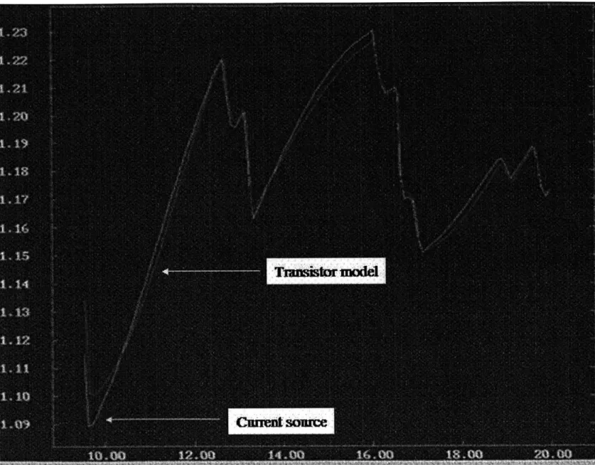
The results are shown in Figure 2.6 and Figure 2.7. While there were slightly higher currents using the current signature, and therefore slightly higher noise voltages, the noise values and current values were certainly comparable. Accordingly, performing simulations using current signatures rather than a transistor-level model seemed to be a reasonable way of simulating the chip.
Needless to say, the current signatures acquired in the previous step were very complicated, piecewise linear functions. I found in simulation that merely using different data inputs, or even reading different addresses in a register array, could lead to different current signatures. This fact is also noted in the literature as a difficulty of obtaining worst-case current signatures [17]. Thus, the critical question was, which current signatures would be used in simulation?
To solve this problem, engineers at IBM typically used triangular current spikes (a model that is used in numerous places in the literature, as cited above). The width of the pulse would be equivalent to the width of the current signature obtained in simulation; the height of the pulse would be chosen so that the total area under the pulse (i.e. the total amount of charge passing through the transistor) would be equivalent to the total area under the current signature curve. I performed several simulations to test whether this was a valid assumption - that is, whether or not a current signature produced a similar noise peak to its triangular equivalent. I found that the answer depended on particular characteristics of the power grid. I will discuss this question in more detail after I present a mathematical analysis of some of the properties of the current sources on chip.
Chapter 3
Mathematical discussion
There are several attempts in the literature [11] [14] [8] [16] to find a closed-form expression for maximum noise due to a particular transistor firing, involving the voltage-current relations for CMOS circuits. Here, I present instead an analysis of a circuit involving an actual current source. I use a current source in this analysis instead of a transistor model for several reasons:
" All of my simulations were done with current sources, so doing a mathematical analysis with current
sources is more illuminating in explaining the results.
" The current source analysis leads to a simpler closed-form result, while still explaining many of the
observations seen in simulation.
" We are not trying to simulate the effect of a single transistor, but rather thousands of transistors firing
in an irregular pattern, so using a transistor might not be illuminating.
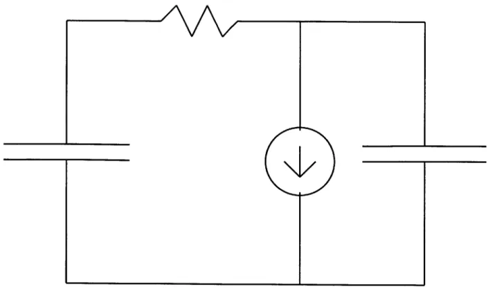
Therefore, consider the circuit in Figure 3.1. We can consider this kind of circuit a rough approximation of what happens on chip when a resistive-capacitive mesh must provide a certain amount of current to a macro. The resistor and left capacitor represent the on-chip resistance and capacitance in the power grid. The capacitor on the right represents decoupling capacitance. There is no resistance between the decap and
Figure 3.1: Simple power grid model
the current source because the resistance between the added decap and the macro is smaller than the on-chip resistance. (The simulations performed also used this model, for simplicity.)
Let Il be the current through the resistor, i be the current through the current source, and V,, be the voltage across the current source. Then - Qback - IR - Qdecap 0. Differentiating with respect to time and
Cback Cdecap
putting Idecap - I1 - i, we get
I1 1+ R d dI1 + I1 =, i
(3.1)
Cback dt Cdecap Cdecap
We can also write an equation for the voltage across the current source, which is identical to the voltage across the decoupling capacitor:
dV 8
Assuming we can put i = kit
+
k2 (the rising half of a triangular current source), we can solve thesedifferential equations for V, yielding
Cback -tk1 k2 k1C2 cR
Vs =-Io R 0
k e nc1c2~ -________ k1ackR ± K (3.3)
Cback + Cdecap Cback + Cdecap 2 Cback + Cdecap (Cback + Cecap )2
where 1o is the initial current that would have been seen without any current source, and K is a constant that allows you to set the initial voltage to any value.
This equation is not exact; the power grid is a distributed network of resistors and capacitors, along with inductive pins connecting the grid to power sources. Therefore, we should not expect this equation to produce an exact solution, but rather a general intuition on how various variables affect the voltage across the current source.
There are several important lessons we can take from this equation.
3.1
Effect of increasing current
First, as the current increases, the voltage across the current source decreases. This can be understood intuitively. There are two different effects that would cause the voltage to decrease:
1. The current across the resistor must be increasing as a function of time. Since the current is proportional
to the voltage, we would also expect the voltage across the resistor to increase as a function of time, serving to depress the voltage across the current source with respect to ground.
2. Because the capacitors are releasing charge, their voltage with respect to ground is decreasing, and so the voltage across the current source will decrease as well.
3.2
Effect of decap on magnitude of peak noise
Second, the addition of decoupling capacitance decreases the extent to which the voltage across the current source will decrease. This can be seen in the equation, as Cdaecap appears in the denominator of every single term; as Cdecap increases, these negative terms become smaller, and therefore there is a lower noise voltage. It
can also be understood intuitively. With more capacitance in the system, providing an equivalent amount of charge will result in less of a voltage collapse, due to the equation
Q
= CV . Establishing a more systematic relationship between the voltage droop and the decoupling capacitance is more difficult; I will discuss this after the next section provides the necessary background.3.3
Effect of decap on time of peak noise
Third, the above equation provides useful knowledge on the time of the voltage peaks. Clearly, as the current rises, the noise voltage will increase. However, eventually the current will reach its peak, and then decrease again. The question is, after the current reaches its peak and begins decreasing, will the noise voltage increase, or decrease? The two effects listed above will now have opposite effects on the noise voltage: Effect
1 will cause the noise voltage to decrease (because the current is decreasing), whereas effect 2 will cause it
to increase (because the current is still positive, so charge is leaking off the capacitors). We must therefore examine the equation in more detail. To do this, we find the rate of change of V,, with respect to time. For simplicity, we can assume that t is relatively large, so we can ignore the exponential term:
dVs -1 k1 C2 R
(klt + k2 + - -back
dt Cback + Cdecap Cback + Cdecap
If we set dV-. dt to 0, and assuming k, is negative and k2 is positive (that is, a positive but linearly decreasing
current), we get
k2 RC2
t back
There are two important things to notice about this equation. First, as Cdeca, increases, the time at which the maximum noise voltage occurs increases. As Cdecap goes to infinity, the time at which the maximum voltage occurs goes to L, which is precisely as we'd expect, since that is the time for which the current is 0
in the equation I = -kit + k2.
In practice, without any decap, when the current starts to decrease, the noise voltage starts to decrease almost immediately. This occurs for two reasons:
1. The package can begin recharging the background capacitance, since the current is decreasing.
2. Other background capacitance further away starts providing charge to recharge the closest background capacitance.
In the context of the above equation, when Cdecap is low, the RCa + c term dominates, so in the
Cback+Cdecap
above equation, t approaches 0 - that is, when the current starts to decrease, the noise voltage decreases as well. However, when decoupling capacitance is added, the RC2ack term decreases. Thus, t rises,
Cback+Cdecap
and with large amounts of decap, t does approach -, or the end of the current spike. This effect will have importance significance, as well be discussed later on.
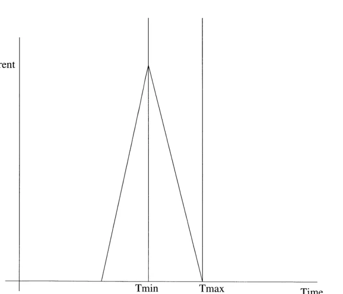
It is important to explicitly spell out one consequence of this observation. At a node containing a current source, the earliest possible time that the peak voltage can occur is the apex of the current source, and the latest possible time is at the end of the current source triangle. Clearly, increasing the amount of current will always cause the voltage droop to increase. Meanwhile, as time elapses with zero current, the capacitors are going to be recharged, so the voltage droop will decrease. Therefore, the peak voltage will always occur in this range of Figure 3.2. The effect of adding decap in simulation, in terms of both decreasing the peak noise and making the peak noise occur later, is shown in Figure 3.3.
3.3.1
Application to determination of peak noise
We can now discuss establishing a quantitative relationship between the peak noise and the decoupling capacitance. Given the equation
Q
= CV, we would want, in principle, to establish a inverse relationshipTmin
Tmax
Time
Figure 3.2: Range of maximal noise
Current
"Aq
iOG
d=-1.7
...
200 dic a-
...
lp
it
-- -- -- -- -- -- -- -- -- -- -- -- . . . . - - - - . . . . - - - - . . . . -- -- -- -- -- -- -- -- -- -- -- -- -- -- -- -- . ... . . . . . . . .- - - . . . . . - - - - . . . . - - - - - - - - - - - --- - - - - - -- - - - - -"UP 700f' OOOPbetween the voltage droop and the capacitance. This equation should hypothetically be of the form V = + ; this can be rewritten as V = 1 + However, according to the above equation,
Cdecap+Cback ground m~de cap +b'
at any specific time t during the ascending part of the current triangle, the voltage will not follow such a relationship. This is because of the presence of the cba cOkR -,t term, which is an inverse-squared
Wbck +0d eca) 2
function with respect to the decoupling capacitance. After the triangle reaches its apex and the current begins decreasing, the sign of k, may change, but the format of the equation will remain the same.
If there is very little decoupling capacitance, as discussed above, the peak voltage occurs at approximately
the same time as the peak current. If we try to plot the inverse of the noise voltage as a function of capacitance at this time, the (c i+ackR 2t term will cause this graph to be superlinear. This means that an inverse
function of the form Vime-of-peak-current = mCc+ will actually overpredict the amount of noise at high
values of the decoupling capacitance.
After extensive simulation, I observed that if we are to put the peak voltage, rather than the volt-age at a specific time, then the equation Vpeakvoltage = mCd1ca+ would hold correctly. Recall that as we add more decoupling capacitance, the time at which the peak voltage occurs increases. Therefore, at low values of decap, Vpeak-voltage is about equal to Vtime-of-peak-current. As the amount of decap in-creases, the time of the peak current inin-creases, and therefore Vpeak-voltage becomes increasingly greater
than Vime-of-peak-current. Therefore, since Vtime-of-peak-current =mCdcc±b overestimates the amount
of noise at large amounts of decap, inserting Vpeak-voltage MCdecap+b1 would probably be a closer fit than
Vtime-of-peak-current mCdeca+b
As it turns out, this produces a nearly perfect fit. So far as I can tell, there is no principled reason for this, other than the heuristic argument above. It just turns out to be an extremely useful approximation, since peak voltages are, very frequently, precisely what we are interested in calculating.
3.4
Effect of pulse width
Fourth, this equation can lend some insight on how noise scales with respect to the width of the pulse. Imagine we were to move the identical amount of charge, but in a shorter window of time; say, instead of a triangle of width 500 ps and height 300 mA, we had a triangle of width 250 ps and height 600 mA. We know that the same amount of charge is being moved, so we would expect the voltage across the background capacitor to be unchanged. However, the charge is moving more quickly, leading to a larger current, so one might expect the voltage across the resistor (and accordingly the voltage across the current source) to compress. Now, imagine we were to have a current spike with the identical peak current, but with a wider base, and hence more charge moved; say, instead of a triangle of width 500 ps and height 300 mA, we had a triangle of width 800 ps and height 300 mA. We know that the peak current is the same, so we will need to maintain the same potential across the resistor. However, we are moving more charge, so the potential across the capacitor will go down. Accordingly, we would expect the voltage across the current source to compress as well. It seems that there are two distinct effects - one related to the peak current, and one related to the total charge.
This intuition is borne out by the equation. Assuming that k2 = 0 and the exponential component is
small, there are two terms which are governed by the slope of the function. The first is the k t 2
Cback±Cdec~jp 2
term. This term is only affected if the amount of charge under the curve changes; multiplying the peak current by N and dividing the peak time by N cause the slope to increase as N2 so the increased slope and the decreased time will cancel out. The second is the (0 C ac t term. In this term, since the t is not
squared, multiplying the peak current by N and dividing the time by N will cause the peak time to increase
by a factor of N. Therefore, even if you have the same amount of charge being passed through the chip,
the voltage droop at the current source will increase. However, the (ca k 2t term is constant with
respect to the peak current. If one were to divide the rise time and fall time of the spike by a factor of N,
but keep the peak current the same, then k, would increase by a factor of N, but the time would decrease
by a factor of N. Therefore, unlike the other term which stayed constant for the same amount of charge, this term stays constant for the same peak current.
In a real-world chip, there is a second reason the voltage droop at the current source increases as you make the current pulse narrower. The charge has to be provided in a given amount of time. RC time constants delay the amount of time in which capacitors far away on the chip can provide charge. Therefore, as the pulse width decreases, the effective capacitance that can provide charge to the current source decreases as well, and so the local voltage droop increases.
However, back to the original equation; we have two factors, one of which changes if the amount of charge changes and is left unchanged by changes in the peak current; and the other of which changes if the peak current changes and is left unchanged by changes in the amount of charge. We can call these terms the "charge term" and the "current term". The question is, which of these terms dominates? This answer is extremely significant, since we need to know how to transform an arbitrary current signature into a triangular current pulse.
To test this, I first performed a series of simulations in which the charge stayed constant, but the peak current changed (Figure 3.4) and then a series of simulations in which the peak current stayed constant, but the charge changed (Figure 3.5). I then compared how the noise changed under either circumstance. According to simulation, it generally appears that the current had a far bigger effect on the noise than the charge under the curve. Put differently, the (k Ck kR )2 t term dominates, as shown in Figure 3.6. Thus,
keeping the current source constant, but altering the width of the pulse, has a relatively small impact on the noise on the chip.
Incidentally, using this analysis, if we were to keep the time constant, and increase the peak current by a factor of N, as shown in Figure 3.7, the peak voltage would also increase by a factor of N. This is because every term in the equation would scale by a factor of N. This is also observed in SPICE simulations.
This knowledge is significant because it calls into question the fundamental assumption of this research
- that we can approximate any current source by a triangular pulse. If the only relevant value is the area under the curve, then any arbitrary piecewise linear current source can be transformed into an equivalent triangular pulse. The same is true if the only relevant value is the peak current. However, if both the peak current and the amount of charge contribute to the noise, then this transformation becomes more difficult.
Current
Time
Time
Figure 3.5: Constant peak current, changing charge
Current
Time
It is unclear whether or not the effects above are actually fundamental to the chip technology, or whether they are artifacts of the way the SPICE model was constructed. In my model, when we place current sources next to resistors, the peak current seems to play a bigger role than the charge. In an alternate model in use at IBM, where current sources are placed next to capacitors, the charge seemed to play a bigger role. The literature cited earlier seemed to suggest that one could determine the amount of charge that the macro would require, and arrange it into a triangular pulse. This would imply that the area under the curve is the only relevant consideration.
Finally, if the peak current (and not just the amount of charge) played a substantial role to the amount of noise, it would have serious implications for circuit design. This is because of the fact that frequently, speeding up a chip results in narrower current pulses with identical amounts of charge under the curves, but taller peaks. If doing this actually caused noise to go up, even with the same amount of charge being moved, it would make speeding up chips difficult.
Chapter 4
Noise propagation trends
In this section, I shall explore the impact of changing chip parameters such as parasitic resistance and parasitic capacitance on noise propagation. I shall also discuss the effects of decap placement on noise. The concepts in this chapter will be critical towards developing a strategy to estimate noise on chip.
4.1
Background capacitance and resistance
Background capacitance and resistance on chip are well-known to slow down chip operation. However, intuitively, increasing background capacitance would also decrease noise, by increasing the amount of charge stored on chip ([1] demonstrates this convincingly). The question is: what is the precise quantitative relationship between background capacitance, resistance, and noise?
The simulated results of this are complicated. The relationships between capacitance, resistance, and noise are quite disparate depending on the distance from the current source. To find these relationships, I did simulations involving a single triangular current pulse, and checked the noise at various locations in its vicinity. The following were the main simulated observations:
* When I checked the noise close to the current source, the noise increased roughly linearly as a function of resistance. The noise decreased when background capacitance increased, but much slower than
inversely; it decreased roughly as an inverse square root.
* As we moved away from the noise source, the noise increased sub-linearly as a function of resistance. Roughly three to four nodes away, the resistance ceased to have almost any effect on the noise what-soever. Meanwhile, as I moved away from the noise source, the relationship between background capacitance and noise fit increasingly well to an inverse curve.
These observations have a relatively straightforward theoretical justification. At the current source, there are two main effects: first, charge is discharging from the on-chip capacitance, and second, it is necessary to maintain a certain level of current across the resistors. Both of these effects will contribute to noise. Earlier,
I presented a graph indicating that the resistive effect was more significant than the capacitive effect, by
comparing the effects of altering the charge (holding the peak current constant) and altering the current (holding the charge constant). Now, if the resistive effect totally dominated, then increasing the resistance would linearly increase the noise (due to V = IR) and increasing the capacitance would have no effect. If the capacitive effect completely dominated, increasing the capacitance would inversely decrease the noise (due to V = 2 and increasing the resistance would have no effect. In reality, increasing the resistance has a slightly sublinear effect, and increasing the capacitance has a sub-inverse effect. The implication is that the resistive effect is more significant than the capacitive effect.
However, as the noise ripples throughout the chip, there are no other current sources which need to maintain a particular current. Accordingly, the main source of noise will arise from capacitors discharging. Now, increasing resistance will result in some additional noise, because increasing the RC time constant will decrease the amount of charge that is released in a certain stretch of time, so voltages will droop in order to compensate. However, the main observed impact of increasing the resistance is that the noise just propagated more slowly through the chip. Accordingly, as one moves away from the noise source, the capacitive effects will dominate. Indeed, several nodes away from the noise source, the capacitive relationship becomes inverse, and increasing the resistance begins to have minimal effect on the actual noise.
under normal conditions, as the on-chip resistance rises, the package begins to contribute a greater proportion of the charge. This trend was also observed in simulation; increasing the resistance at small values of the
resistance had a greater effect than increasing the resistance at large values of the resistance, and at a certain point increasing the resistance had minimal effect.
The implications of this analysis are as follows:
1. In general, the relationship between capacitance, resistance, and noise is complicated at various nodes
on the chip. This was one of the factors that led me to use precharacterization, rather than closed-form mathematical analysis, in order to create a noise estimation procedure.
2. Increasing background capacitance or background resistance can be an effective strategy to battle noise voltage, but only under certain circumstances. If the goal is to minimize the noise around a sensitive node far away from the main sources of noise, then increasing the surrounding background capacitance might have a pretty fair impact, but decreasing the resistance in the power grid would not have an effect. Conversely, close to sources of noise, decreasing the resistance in the power grid can have very significant impacts on the noise.
4.2
Noise modeling on chip
In this section, I will expand on the initial discussion of noise in the context of a single RC circuit. I will discuss experimental observations and corresponding theoretical models of noise propagation on chip. All of the insights in this section will be necessary in the next section, which will discuss accurate ways of evaluating the total noise at any node on chip. This noise evaluation technique is the center of the decap estimation
algorithm discussed at the end of this thesis.
4.2.1 Superposition
We saw in the last section that the total noise in the RC circuit was linearly proportional to the magnitude of the current peak, assuming the current width remains constant. In general, when solving circuits with
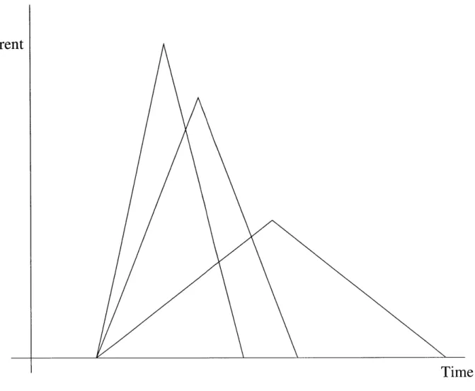
numerous current sources, their effects can be added linearly; we can treat each current source individually, and sum their resultant noise values. This suggests a general principle of superposition, in which the total noise due to several current sources is equivalent to the total noise due to each individual current. Indeed, this principle of superposition holds in SPICE analysis. The significance of this is that to determine the noise at any point on chip, we only need to fully characterize the noise due to a single current source. We can then linearly add the noise due to each current source to obtain the true value. An example of superposition at work can be seen in Figure 4.1. In this figure, the bottom curve represents the noise due to three current sources firing together; the other three curves represent the noise due to each individual current source firing on their own. The bottom curve can be seen to represent the sum of the other three curves.
However, superposition does not work for capacitors. It is apparent from the equations determined in chapter 3 that adding capacitance does not have corresponding linear effects on the noise; indeed, there is a diminishing marginal impact of adding additional capacitance. Consequently, knowing the effect of placing
N capacitors alone in location 1, and the effect of placing M capacitors alone in location 2, cannot be used
to determine the effects of playing N capacitors in location 1 and M capacitors in location 2. This is the main difficulty of the noise estimation problem.
4.2.2 Noise propagation
In simulation, it generally appeared that the peak noise due to a current pulse decreased roughly as the inverse square of the distance to the current pulse, as can be seen in Figure 4.2. This trend can be explained
by the following theoretical model. We can imagine that the noise travels along the chip at a certain speed.
When the noise wave reaches some node N at a distance d of the source, all nodes of distance d or closer to the source will have been affected. In reality, what is occurring is that charge stored on capacitors on outlying nodes recharge capacitors on inner nodes until an equilibrium is reached. So for instance, the capacitors at distance 2 will recharge the capacitors at distance 1 until an equilibrium between these two sets of capacitors is reached; as the capacitors at distance 2 discharge, the capacitors at distance 3 will recharge them until an equilibrium is reached; and so the noise is spread through the chip.
... ... ... ... ... ... -ij i. P-i w - - - -- -- - - - . ... . . . .A - - - - ---% .. . . . . . . . .. . .. . ./ - - - -. -. -. -. -. -. -. -. -. -. . . . . .. . . .. . . . . . .. . . . . . . . . . . ... . . . . . k . . . . . . . . . . . . ../ . . . . .. . .. . . . . . . . . . d - - - - --- - - -L L - -. -. -. -. -. -. -. -. -. -. -. -.. . . ... . . . ... . . . . . . .. . . . . ! . . . .. . . . . . .. . .. . . .I ... .. .... ... .. ..... . ... . ...... ... ... . . . . . . . . . . . .. . . . . .1 -. -. -. -. -. -.. . . . . . . .. . . .. . . . .. . . . . . . . . . . . ... . - - - - --- - - - -- - - . . . .. . . . ... . . . . . . .. . . ... . . . . . . . . . 40ft 7OW IS
It is therefore reasonable to imagine a model where, as noise spreads to a distance d, the noise is distributed across all nodes of a distance d. Since we are using a two-dimensional grid, the total number of nodes within a distance d is proportional to the area of the circle of radius d, and thus increases with the square of the distance from the source. Accordingly, we would expect the noise to drop off as roughly an inverse square, as the above graph indicates.
This fact is of extreme importance in developing a noise propagation model, for two reasons. First, it can allow us to estimate the noise from far-away current sources with reasonable accuracy, given the noise from nearby current sources. However, more significantly, it implies that noise drops off extremely rapidly, so that the vast majority of the noise from some current source will come at the very node at which the current source is located. Experimentally, consider a setup like Figure 4.3. This produces significantly more noise at the side, top and bottom nodes than at the middle node. (The middle node does experience more noise than the corner nodes, however). The implication of this is that for any realistic distribution of current sources on chip, if we are able to substantially reduce the noise exclusively at the current source nodes, it is very likely that we have substantially reduced the noise everywhere. Put differently, assuming that our noise tolerance is constant at every node on chip, it suffices to reduce the noise to within acceptable limits exclusively at nodes which contain current sources, because we can then infer that all nodes are within acceptable limits.
(If nodes have different noise tolerances, however, this assumption becomes invalid.) This fact will be used
to substantially reduce the runtime of the eventual decap allocation algorithm.
4.2.3
Effect of decap on noise propagation
As discussed in the previous section, noise propagates through the chip radially from the original source of noise. Adding decoupling capacitance has the effect of reducing the noise by a certain fraction. One critical question in the placement of decoupling capacitors is: to what extent does the location of the decaps affect the noise propagation?
The first series of experiments to answer this question were performed by placing a current source at some node N, and measuring the noise at some measurement point M. I placed capacitors at every
inter-I,
N
Figure 4.3: Hypothetical current source setup
Q
N
rF*"
r-""
Location
1Location2
(
Figure 4.4: Placing decaps in various locations
Location 3
mediate location. So, in Figure 4.4, the effect of decoupling capacitance at each location would be measured individually.
The following observations were made:
" Decoupling capacitors placed at the current source (Location 1) produced the identical effect as
de-coupling capacitors placed at the measurement point (Location 3).
" Decoupling capacitors placed at intermediate locations (e.g. Location 2) produced a slightly smaller
effect than decoupling capacitors placed at either Location 1 or Location 3.
" Decoupling capacitors placed outside of the line of sight between the current source and the
measure-ment point (e.g. in a hypothetical node to the left of Location 1) had a far smaller effect.
These observations can be explained using a theoretical model suggested in Figure 4.5. Adding decoupling capacitance attenuates the noise wavefront by a certain ratio. Whether this attenuation occurs early or late in the wavefront propagation does not affect the degree of attenuation. So in the above example, imagine that moving a single node away from the current source causes the noise to attenuate by a factor k, i.e.
N
k
Imagine that adding some decap causes the noise to attenuate by a factor q. Consider the noise two nodes away from the current source. Then, placing the decoupling capacitance at the current source would
Figure 4.5: Noise propagation model
Measurement
p ioint
cause the noise to attenuate as
N/q N
k k2q
Whereas, placing the decap at the measurement point would cause it to attenuate as follows:
N N
N -> - Iq = k k2q
Both of these equations, however, result in a total noise N. That is, placing decap at the measurement point is equivalent to placing it at the current source.
One might wonder why the same would not be true for decaps placed in intermediary positions between the current source and the measurement point (for instance, Location 2 in the above diagram). The answer is, as the diagram suggests, there are numerous paths for the noise to take between the current source and the measurement point. Placing the decap at Location 2 only attenuates one path, while placing it at Locations 1 or 3 attenuates all of the paths. However, the shortest path travels fewer nodes than the second shortest path (three as opposed to five in the above example). Accordingly, adding decap in Location 2 has a very similar impact to adding decap in Location 1, a fact we will exploit in the noise estimation algorithm.
The final question is the effect of decaps outside of the line of sight. According to the wave propagation model, a decap placed to the left of the current source would have no impact whatsoever. This is false; adding decap there does help replenish the capacitors at the current source, and therefore does have an effect on the noise throughout the chip. However, decaps outside of the line of sight have a less significant impact than decaps in the line of sight, which is also a fact that will have to be taken into account.
4.2.4
Distribution of capacitance among nodes
Consider the five different situations in Figure 4.6. In the earlier section, I described how situations 1 and
5 would produce the identical impact at the measurement point. Similarly, situations 2 and 4 produce
Ni decaps
Situation 1: Ni
Situation 2: NI
Situation 3: Ni
Situation 4: Ni
Situation
5:
NI
N2 decaps
=
0,
N2
=
20
= 5, N2 = 15
=
10, N2 = 10
= 15, N2 = 5
=
20, N2
=
0
capacitance is the same, does the distribution of this decoupling capacitance affect the total noise at the measurement point?
The answer to this question is yes, which complicates the question considerably. The reason is that we've already seen that there is a diminishing marginal impact to adding capacitors at a node. Consequently, consider a situation in which there are 10 decaps at the current source, and 0 decaps at the measurement point. Adding 10 additional decaps at the current source (yielding situation 5) will have less of an impact on the noise than adding 10 decaps at the measurement point (equivalent to situation 3), because there is a diminishing marginal impact to adding more decap at Location 1.
Accordingly, spreading decap out evenly (i.e. situation 3) has two impacts:
1. The noise at the measurement point will tend to be lower.
2. The peak at the measurement point will occur somewhat later.
We will call this effect the "double node effect".
In SPICE simulation, effect 2 was far more noticeable than effect 1, as Figure 4.7 indicates. In fact, there was minimal impact on the noise peak, and in fact the noise appears slightly greater in situation 3 (for reasons that are not entirely clear). However, it is very clear that the time at which the peak occurs is far greater. To explain the significance of this, let the time of the peak noise in situation 1 and 5 be tp. At time t,, the noise associated with situation 3 is significantly less than the noise associated with situations 1 and 5. Accordingly, even if the peak noise is not much affected by the distribution of capacitors, the noise at specific times is affected.
In general, on chips, we may have several dozen current sources, all firing at the same time. The noise at any given node is the superposition of the noise due to each of these current sources at that node. It turns out that it is fairly easy to approximate the peak noise due to each of these current sources at that node. However, attempting to add these values linearly will grossly overestimate the noise, since these peaks occur at radically different times. Overcoming these time shifts is the main challenge in approximating the noise at any node.
. .. .. .. .. ... .. .... . . .. .. .. .. . .. .. . ... . . .. ... .. .. 14 ---ahowl ---41 5t 41 ... ... ... ... ...
'SftWim 3
... ...
. . . .. . . . . . . . . . . .. --- ... ... ... 4000 soonChapter 5
Noise approximation
5.1
Problem description
In this section, I will describe my solution to the problem of finding the noise at any node, due to an arbitrary collection of current sources and decaps scattered throughout a chip. This problem is not merely academic; this approximation is the core of the next chapter, which describes an algorithm to actually place the correct
amount of decaps at every node on the chip.
Let us spell out the problem in more detail. Consider the scenario in Figure 5.1. The question we are trying to answer is as follows. What is the value of the noise, at any of the nodes, as a function of N1, N2,
and N3? N1 will affect the value of the noise at all three nodes, N2 will affect the value of the noise at all
three nodes, and N3 will affect the value of the noise at all three nodes. We need to determine the noise at
all nodes, as a function of the decap at all nodes.
Noise estimation with decap has been studied numerous times in the literature. [11], [14], [8] and [16] all
make accurate calculations at the transistor level, a level of abstraction which is too low for our purposes. A direct differentiation model is suggested in [10], which does not appear to take into account the diminishing effect of decaps at different distances from the noise source. [19] calculates the noise with the assumption that all of the charge comes from the pins, and calculates the IR drops from the pins to the current sources;