HAL Id: tel-00815161
https://tel.archives-ouvertes.fr/tel-00815161
Submitted on 18 Apr 2013HAL is a multi-disciplinary open access
archive for the deposit and dissemination of sci-entific research documents, whether they are pub-lished or not. The documents may come from teaching and research institutions in France or abroad, or from public or private research centers.
L’archive ouverte pluridisciplinaire HAL, est destinée au dépôt et à la diffusion de documents scientifiques de niveau recherche, publiés ou non, émanant des établissements d’enseignement et de recherche français ou étrangers, des laboratoires publics ou privés.
Développement et fabrication de transistors couches
minces verticaux en technologie silicium polycristallin
basse température
Peng Zhang
To cite this version:
Peng Zhang. Développement et fabrication de transistors couches minces verticaux en technologie silicium polycristallin basse température. Electronique. Université Rennes 1, 2012. Français. �NNT : 2012REN1S156�. �tel-00815161�
N° d’ordre : ANNÉE 2012
THÈSE / UNIVERSITÉ DE RENNES 1
sous le sceau de l’Université Européenne de Bretagnepour le grade de
DOCTEUR DE L’UNIVERSITÉ DE RENNES 1
Mention :ÉLECTRONIQUEEcole doctorale Matisse
présentée par
Peng Zhang
Préparée à l’IETR, UMR 6164
Institut d’Electronqiue et des Télécommunications de Rennes
U.F.R. Structure et Propriétés de la Matière
Development and
Fabrication of
Vertical Thin Film
Transistors Based on
Low-Temperature
Polycrystalline
Silicon Technology
Thèse soutenue à Rennes le 18 Décembre 2012
devant le jury composé de :
Henri HAPPY
Prof. IEMN, Université de Lille / rapporteur
Thomas ERNST
HdR, Dr. Ing. CEA, LETI Minatec Grenoble / rapporteur
Wei LEI
Prof. Université du Sud-Est, Nankin, Chine / examinateur
Tayeb MOHAMMED-BRAHIM
Prof. IETR, Université de Rennes 1 / examinateur
Gaël GAUTIER
HdR, MCF, Université de Tours / examinateur
Emmanuel JACQUES
MCF Université de Rennes 1 / examinateur
Olivier BONNAUD
Prof. Université de Rennes 1 / directeur de thèse
Régis ROGEL
Acknowledgements
Acknowledgements
The work presented in this dissertation cannot be achieved without the contribution of many individuals. These people deserve my most sincere gratitude for their assistance during my three years’ doctoral study in the University of Rennes1.
First, I would like to thank one of my advisors, Professor Olivier BONNAUD, for providing me this valuable opportunity to be able to study in the microelectronics field in IETR, which may be a critical step in my career. His insightful guidance has helped me to determine the work objective and direction, his rich experience has always helped me to analyze the experimental data, and his optimistic attitude has encouraged me to fulfill this work.
Second, I would like to thank the other research advisor, Mr. Régis ROGEL, for his devotement throughout the fabrication process and the results analysis. His preciseness and well-planning in the scientific research has helped me to continuously focus on this work and carry on the work step by step, his professional knowledge has helped me to solve technological problems, and his diligence has always encouraged me.
I also would like to thank the group member, Mr. Emmanuel JACQUES, for his assistance in the fabrication process and kind discussions. His constructive opinions in the discussions have always helped me to solve problems during my three years’ study, he has also helped me with the theoretical analysis, and his considerable knowledge has always benefited me.
Special thanks owe to the jury members of the defense. I would like to thank the reporters, Mr. Henri HAPPY, professor in IEMN at the University of Lille 1, Mr. Thomas ERNST, “HdR” and “Dr. Ing.” from CEA in LETI-Minatec in Grenoble, and the reviewers, Mr. Wei LEI, professor at the Southeast University in China Nanjing, Mr. Tayeb MOHAMMED-BRAHIM, professor in IETR at the University of Rennes 1, Mr. Gaël GAUTIER, “Maître de Conférences HdR” at the University of Tours, for spending time reading this thesis and giving their valuable comments, which will be very educational and edificatory for the future work.
All the professional members in the department of Microelectronics and Microsensors are acknowledged, for their contributions to the processes and their helpful discussions, and their hospitality and humor make my doctoral study more interesting and enjoyable. Special thanks go to Professor Laurent PICHON, for providing me with the financial support for the recent
Acknowledgements
three months, and for his kind help during the three years’ study. Special thanks also go to Olivier DE SAGAZAN for his assistance in LPCVD, oxidation, etching and other operations, and for his kind and helpful discussions. I also would like to thank Aurélie GIRARD for helping me with all kinds of procedures for the thesis, especially for helping me with submitting the thesis to the jury members, and I also want to thank Maxime HARNOIS for examining my thesis. The technicians, Mr. Christophe LEBRETON, Mr. Jean-Michel BOT, and Mr. Xavier MORVAN are also specially acknowledged for their assistance in the clean room work and during the fabrication process. My special thanks also go to the secretaries, Mrs. Fabienne JEGOUSSE, Mrs. Isabelle CHOUANNIERE, Mrs. Claire MALET, and Mrs. Nathalie COLLIN, for their kind help throughout my doctoral study. Outside of the laboratory, I would like to specially thank Mr. Joseph LELANNIC for providing abundant SEM images.
I will not forget the previous and current colleagues in the laboratory, Himi Deen TOURE, Khaled BELARBI, Bruno DA SILVA RODRIGUES, Isman SOULEIMAN, Fouad DEMAMI, Abdehani KHERRAT, Liang NI, Sabri JANFAOUI, Gertrude GODEM WENGA, Ismail BOUHADDA, Lamine SAMB, Maxime THOMAS, Yannick KERVRAN, Hanpeng DONG, Sarah BEBICHE, Mahmoud ISRAEL, and so on, for spending so much happy time together. My special thanks go to Ni Liang, for his kind help in and outside of the laboratory, his experience has been very helpful for my study and living here. My special thanks also go to Himi Deen TOURE, he has taught me the basic fabrication process of VTFTs at the beginning of my study here. I also need to specially thank Bruno DA SILVA RODRIGUES, thank his wife and him for their hospitality during my stay in Brazil. I also need to thank Sabri JANFAOUI for helping me with all kinds of procedures for the thesis.
I will also not forget the other friends outside of the laboratory, Lin ZHANG, Yuechun SHI, Pan TANG, Zongqing LU, Lv WANG, Guang YANG, Xiaoyan HE, Yang CHEN, Jiasong WU, Gang ZHOU, Cong BIAN, Chenfeng YANG, Shuai YANG, and so forth. Thank you for always helping and supporting me, and making my life more colorful.
At last, I would like to thank my family, my mother, my father, and my elder sister. I cannot express my gratitude for their always care, devotement, encouragement and support since I was born, and I just dedicate this work to them with my sincere wishes!
Table of contents
Table of contents
General introduction ... 1
Chapter 1 Introduction ... 5
I. Development and revolution of MOSFETs ... 6
II. Lateral Thin Film Transistors (LTFTs) ... 7
III.1 Introduction of LTFTs ... 7
III.2 Fabrication process of LTFTs ... 8
III.3 Basic working principle of LTFTs ... 11
III. Three-dimensional FETs: FinFETs and other alternative structures ... 15
III.1 Introduction of FinFETs ... 15
III.2 Basic working principles of FinFETs ... 16
III.3 Advantages of FinFETs and technological challenges... 17
III.4 Alternative three-dimensional structures ... 19
IV. Vertical transistors: vertical MOSFETs and vertical TFTs (VTFTs) ... 22
IV.1 Introduction of vertical MOSFETs ... 22
IV.2 Introduction of VTFTs ... 24
IV.2.1 Comparison between LTFTs and VTFTs ... 25
IV.2.2 State of the art for VTFTs ... 26
V. Conclusion ... 28
Chapter 2 Related techniques, process flows, and electrical characteristics of the classical VTFTs ... 31
I. Related materials and techniques in thin film technology ... 32
I.1 Introduction of different silicon structures: mono-Si, a-Si and poly-Si ... 33
I.2 Poly-Si deposited by LPCVD technique ... 37
I.2.1 LPCVD principle ... 37
I.2.2 In situ doping for LPCVD ... 39
Table of contents
I.2.3.1 Common crystallization methods... 41
I.2.3.2 Conventional thermal annealing ... 42
I.3 Silicon nitride (Si3N4) films deposited by LPCVD technique ... 42
I.4 Atmospheric Pressure Chemical Vapor Deposition (APCVD) technique ... 43
I.5 Joule effect evaporation of aluminum (Al) ... 44
I.6 Reactive ion etching (RIE) for patterning ... 45
II. Classical VTFT structure, process and technological challenges in the process ... 46
II.1 Detailed process flow for the classical VTFT structure ... 47
II.2 Technological challenges for the sidewalls formation – RIE parameters adjustment ... 51
III. Electrical characteristics and improvements on the classical VTFTs ... 53
III.1 Electrical parameters deduction ... 53
III.2 Electrical characteristics of the first classical VTFTs ... 54
III.3 Parasitic channel suppression for the classical VTFT structure ... 55
III.3.1 Modification of the fabrication process ... 56
III.3.2 Geometric definitions of the improved classical VTFT structure ... 57
III.3.3 Electrical characteristics of the improved classical VTFT structure ... 59
III.3.4 The effect of geometric parameters on the electrical characteristics ... 61
III.4 Overlapping area reduction and corresponding characteristics ... 64
III.4.1 Modification of the fabrication process ... 64
III.4.2 Electrical characteristics of the classical VTFT with reduced overlapping area ... 65
IV. Conclusion ... 67
Chapter 3 Process flows and electrical characteristics of the new VTFTs ... 69
I. Transition from the classical VTFT to the new VTFT... 70
I.1 Discussion on the classical and the new VTFTs ... 70
I.2 Simulation of the two VTFT structures ... 71
II. Structure, process, and key technique of the new VTFT structure ... 73
Table of contents
II.2 Geometric definition of the new VTFT ... 77
II.3 Key technique: barrier layer selection ... 78
III. New VTFTs based on a 100 nm SiO2 insulating layer between source and drain ... 80
III.1 Technological challenge in the process - sidewall formation by RIE ... 81
III.2 Electrical characteristics of the new structure with a 100 nm SiO2 insulating layer ... 83
III.3 Analysis of the field effect mobility ... 86
III.4 Technological problem in the process – “shadow effect” in Al deposition ... 88
IV. New VTFTs based on a 200 nm Si3N4 insulating layer between soruce and drain ... 89
IV.1 Technological challenges in the process – sidewall formation by RIE ... 90
IV.2 Electrical characteristics in comparison with the VTFTs with a SiO2 insulating layer ... 91
IV.3 The effect of geometric parameters on the electrical characteristics ... 94
V. New VTFTs with different active layers ... 95
VI. P and N-type VTFTs ... 98
VI.1 Electrical characteristics of P and N-type VTFTs... 99
VI.2 The Effect of geometric parameters on the electrical characteristics ... 101
VI.2.1 P-type VTFT ... 101
VI.2.2 N-type VTFT ... 102
VI.2.3 The effect of geometric parameters on the ION/IOFF ratio ... 104
VII. Conclusion ... 104
Conclusion and perspectives ... 107
References ... 113
Publications ... 123
Annexes ... 125
Annex I RCA cleaning ... 126
Annex II Photolithography ... 127
Annex III Masks design ... 128
General introduction
1
General introduction
The scale-down of CMOS technology has followed Moore’s law for around a half century, especially for the recent two decades, the doubling of transistors has continuously taken place every eighteen or twenty-four months. However, when CMOS is scaled into sub-100 nm regime, it has already shown short channel effects (SCEs), which limits the electrical performance of CMOS devices and circuits. When the micro processor unit (MPU) node shrinks to 16 nm expected in 2013, more problems may emerge. On one hand, quantum tunneling will result in large leakage, regardless of the adopted materials. On the other hand, higher resolution requirements in the lithography and plasma etching techniques prohibit the reliability of the fabricated devices. Therefore, new FET architectures should be proposed.
The three-dimensional (3D) FET has been proposed ahead of time, i.e., Intel Corp. proposed the tri-gate FinFET in 2011 and adopted it in the 22 nm node CPU. Due to the wrapped gate of FinFET that could provide better electric field controlling, the leakage current has reduced one order of magnitude due to the coupling of the gates (work as a double-gate FET), in comparison with the 32 nm planar FET. This result has indicated the advantage of the 3D FET, and a lot of other 3D FET structures have also been proposed, including the inverted-T channel FET, the Omega-gate FET, the Pi-gate FET, the four-gate FET, the Gate-All-Around (GAA) FET, and so forth. However, on one hand, due to the more complex process, these alternative 3D structures have not yet been adopted. On the other hand, including FinFET, these 3D structures are still limited by the lithography and plasma etching techniques. In addition, the high sidewall roughness observed from FinFET has been a common technological challenge for the 3D FETs.
Another FET structure has been proposed by rotating the planar FET 90°, so-called “vertical FET”. On one hand, the channel length of this vertical structure is determined by the deposited layer thickness between source and drain, thus it is independent of the lithography technique. On the other hand, the ultra-short channel length could be obtained with a large channel width, which enables to increase the drive current. In addition, the vertical architecture also enables to realize a double-gate or multi-gate structure, which further
General introduction
2
improves the electrical performance. Therefore, vertical FET is also a promising structure to pursure Moore’s law.
In the laboratory of IETR, thin film technology has been well developed, with different thin film materials and deposition techniques. Especially for polycrystalline silicon (poly-Si), mature low pressure chemical vapor deposition (LPCVD) and solid phase crystallization (SPC) techniques have been adopted for low-temperature (T ≤ 600°C) thin film transistors (TFTs) fabrication. Therefore, our laboratory has proposed a vertical thin film transistor (VTFT) structure based on this low-temperature poly-Si technology. This thesis deals with the research on this special VTFT structure. The organization of this thesis is shown below:
In the first chapter, the state of the art for the new FET structures will be introduced. Initially, the scale-down tedency of MOSFETs will be presented. Afterwards, the fabrication process of the lateral thin film transistors (LTFTs) will be given step by step, and the work principle of a MOSFET will also be presented based on the LTFT. Subsequently, different 3D structures, including FinFET, will be given. At the end of this chapter, vertical FET structure will also be proposed, with its advantages over the planar FET structure.
In the second chapter, the VTFT structure will be proposed by rotating LTFT 90°. Different thin film materials and techniques adopted in the fabrication process will be detailed, especially for the low-tempertaure poly-Si technology. Afterwards, the fabrication process of the classical VTFTs will be presented in detail step by step. Static electrical measurements will be shown and analyzed, highlighting some problems related with the proposed VTFT architecture, and some solutions will also be given to improve the electrical properties by modifying some steps of the technological process.
In the third chapter, a new VTFT structure will be proposed, in order to radically solve the problems in the classical VTFT structure. Initally, the theoretical analysis of this new structure will be presented. Subsequently, the fabrication process of the new VTFT structure will be shown step by step. The technological challenges of the new VTFTs will be given, and the electrical characteristics will be presented and analyzed, in comparison with the electrical properties of the classical VTFTs. Based on the analysis of the electrical characteristics of the
General introduction
3
fabricated VTFTs, several attempts will be made to improve the electrical characteristics step by step. Moreover, P and N-type VTFTs will be fabricated, highlighting the feasibility of a CMOS-like VTFT.
Finally, we will conclude the study on poly-Si VTFTs, and we will also present some perspectives for future work on our VTFTs.
Chapter 1 Introduction
Chapter 1 Introduction
6
I. Development and revolution of MOSFETs
Since the first MOSFET was fabricated in 1960 by D. Kahng and M.M.Atalla of Bell Telephone Laboratory [1, 2], the semiconductor industry has undertaken a tremendous revolution based on CMOS circuits. The scale-down of the planar transistors has followed Moore’s law for around half century, especially for the recent two decades, the doubling of transistors has continuously taken place every eighteen or twenty-four months [3, 4]. However, the scale-down tendency will see its restriction when the micro processor unit (MPU) node shrinks to 16 nm expected in the 2013 timeframe of the International Technology Roadmap for Semiconductors (ITRS) shown in figure 1-1 [5]. This limitation is mainly due to two reasons: on one hand, quantum tunneling due to the short channel length would enlarge the leakage as well as serious short channel effects (SCEs), regardless of the adopted materials. On the other hand, the high resolution requirements in the lithography and plasma etching techniques prohibit reliable and mass production. Therefore, new FET architectures should be proposed and adopted in order to break through this limitation.
Figure 1-1: Evolution of the MPU node provided by ITRS 2010, the 16 nm node was expected
in 2013.
Fortunately, the semiconductor industry has found the solution for overcoming the former challenge of leakage ahead of time, by adopting the new three-dimensional transistors (3D transistors), which enable to form wrapping gate structures. Intel Corp. announced its tri-gate FinFETs manufactured at 22 nm in 2011 [6, 7], which greatly improves the electrical
Chapter 1 Introduction
7
characteristics in comparison with its 32 nm planar transistors. FinFETs for 16 nm manufacturing process are also being developed by Intel, IBM, Samsung, Toshiba and other corporations [8 - 11].
Another concept of 3D FETs, the vertical MOSFETs has also been proposed by rotating the planar MOSFETs 90°, thus the channel length could be defined by a non-lithography method instead of improving the lateral resolution [12, 13], which would enable to simplify the process. In addition, for the vertical MOSFETs, the leakage could also be well-controlled by introduction of the multi-gate structure. In summary, vertical MOSFETs could be another classification of promising FETs to pursue the Moore’s law.
Considering the thin film technology, thin film transistors have also been developed to pursue this scale-down trend. Not only the lateral thin film transistors (LTFTs) have been developed corresponding to the planar MOSFETs, but a lot of 3D thin film transistors have also been proposed, including vertical thin film transistors (VTFTs), which correspond to vertical MOSFETs.
II. Lateral Thin Film Transistors (LTFTs)
III.1 Introduction of LTFTs
Before the description of different three-dimensional FETs, the basic principle of the MOSFETs should be presented by taking the traditional planar transistors as an example. As the wide usage of the thin film technology, the lateral thin film transistors (LTFTs) have been researched for about a half century [14-16]. In the microelectronics laboratory in IETR (Institut d'Electronique et des Télécommunications de Rennes), lateral thin film transistors (LTFTs) have also been fabricated and studied for over a decade [17, 18]. Based on the LTFTs technology, the prototype of the vertical thin film transistors (VTFTs) will be proposed.
In this section, the simplified fabrication process of LTFTs is shown step by step. Afterwards, the basic working principle of transistor will be expressed by taking the LTFT as an example, and the typical transfer and output characteristics of the LTFT will also be analyzed.
Chapter 1 Introduction
8
III.2 Fabrication process of LTFTs
In our laboratory, the fabrication of the LTFTs (N and P-type) is based on the fabrication process of the planar MOSFETs. For the planar MOSFETs, the source, drain and channel parts are formed in the monosilicon body, and the doping is achieved via high-temperature diffusion or ion implantation methods.
In contrast, all the parts of the LTFTs are formed by using silicon thin film technology. Among the different silicon deposition techniques, LPCVD technique has been proved to have the largest grain size and the best reliability by involving the solid phase crystallization (SPC) technique. In addition, for LPCVD, the source and drain could be in situ doped by dopant injection during the deposition process. Therefore, this mature low-temperature LPCVD technology has been widely used for our LTFTs fabrication [19, 20]. Moreover, the process can be fully compatible with the glass substrates, as the maximum temperature can be limited to 600°C. Therefore, it enables the applications in the display field, such as the active matrix liquid crystal display (AMLCD), the active matrix organic light-emitting diode (AMOLED) [21 - 23], and so on.
The fabrication of the LTFTs could be achieved either by a bilayer method, or by a monolayer way [24]. For the bilayer method, the source and drain heavily-doped layers (labeled as “N+”) are deposited after the definition of the active layer (labeled as “Undoped”) by an etching step (the two layers are not deposited at the same time), while for the monolayer method, the two layers are continuously deposited prior to the definition of the active layer, which can be shown in figure 1-2 (a) and figure 1-2 (b), respectively.
Chapter 1 Introduction
9
Note that, for the monolayer method, due to the continuous depositions of the two layers, the interfacial defect densities between the two layers are much less than the ones for the bilayer method. Therefore, the fabrication of the monolayer LTFTs will be described in detail with a four-mask process [25].
The fabrication process of the LTFTs begins with the deposition of the buffer oxide. After cleaning the substrates, a thick 500 nm silicon oxide layer is deposited by Atmospheric Pressure Chemical Vapor Deposition (APCVD) method. The LTFTs are fabricated on this buffer oxide layer, and thus the devices could also be isolated from each other.
Afterwards, the polycrystalline silicon (poly-Si) layers are deposited by the Low Pressure Chemical Vapor Deposition (LPCVD) technique. After the deposition of a 150nm undoped poly-Si layer, another 150nm N-type highly-doped poly-Si layer is continuously formed by in
situ doping using phosphine gas PH3 (while P-type poly-Si layer is formed by in situ doping
using diborane gas B2H6). Due to the same processing flow of the N and P-type LTFT, the
fabrication process of the N-type LTFT is taken as an example, and the schematic structure for the deposited layers is shown in figure 1-3:
Figure 1-3: Schematic structure after the deposition of two poly-Si layers by LPCVD
technique. “N+” stands for the N-type heavily-doped poly-Si layer, and “poly-Si” stands for the undoped poly-Si layer.
After the deposition of the two poly-Si layers, the first mask is used and then the first reactive ion etching (RIE) is carried out to form poly-Si islands, as shown in figure 1-4. For each LTFT, source, drain and the active layer will be included in the same island, thus the size of one single LTFT is determined by the island dimension.
Chapter 1 Introduction
10
Figure 1-4: The first RIE step to form the poly-Si islands, whose dimensions would determine
the sizes of the LTFTs.
After the definition of the poly-Si islands, the second mask is used and a second RIE is carried out to etch the N-type heavily-doped poly-Si layer (labeled as “N+”) until reaching the interface between the heavily-doped poly-Si layer and undoped poly-Si layer (labeled as “Poly-Si”), and thus source and drain are formed for each LTFT, which is shown in figure 1-5:
Figure 1-5: The second RIE is carried out to form source and drain of the LTFTs.
Before the deposition of the gate oxide, a standard RCA cleaning is necessary in order to eliminate most of the impurities at the interface between the undoped poly-Si layer and the gate oxide, as the channel would be formed near this interface. Thus, RCA cleaning enables to improve the electrical characteristics of the fabricated LTFTs.
After the RCA cleaning, a 100 nm SiO2 thin film layer is deposited by APCVD technique
followed by a densification process at 600°C for at least 12 hours. Afterwards, a third mask is used and wet etching is carried out to make contact openings for source and drain. The final schematic structure after gate oxide deposition and wet etching is shown in figure 1-6:
Chapter 1 Introduction
11
Figure 1-6: Gate oxide deposition and wet etching to make contact openings.
The final step is the formation of aluminum (Al) contacts for source, drain and gate. After the deposition of a 300 nm Al layer by Joule effect evaporation method, the source, drain and gate contacts are formed by wet etching using the fourth mask. The final schematic structure of the fabricated LTFTs is shown in figure 1-7:
Figure 1-7: Schematic structure of the final LTFTs, the deposited Al is etched and the contacts
are formed.
As mentioned above, except for the fabrication of the N-type LTFTs, P-type LTFTs are also fabricated in our laboratory, and thus the P and N-type LTFTs could be complementarily arranged on the same substrate (so-called “CTFTs”), which corresponds to the CMOS technology [26]. Based on the CTFTs technology, the CTFT inverters are achieved, and other circuits based on LTFTs are also fabricated [27].
III.3 Basic working principle of LTFTs
Corresponding to the classical MOSFET, the schematic of a single N-type normally-off LTFT using thin film technology is shown in figure 1-8. For the gate part, the multi-layer Al/SiO2/poly-Si also forms the Metal-Oxide-Semiconductor (MOS) structure, thus the
Chapter 1 Introduction
12 planar MOSFETs.
Figure 1-8: Schematic view of the N-type normally-off LTFT.
In order to simplify the explanation of the working principle, the three-dimension schematic for the gate part of the N-type normally-off LTFT is shown in figure 1-9, source and drain are at the left and right part of the undoped poly-Si (not shown in figure 1-9), and the channel will be formed in the area below the gate oxide and the gate metal contact. The important geometric parameters for the LTFT are listed below:
- L: channel length, determined by the gate coverage length from source to drain;
- W: channel width, determined by the gate coverage width perpendicular to the channel
length L;
- TOX: the thickness of the gate oxide layer;
- Tsi: the thickness of the undoped poly-Si layer, determining the depletion type of the LTFT (full depletion or partial depletion).
Figure 1-9: The MOS structure of a LTFT, the geometric parameters are shown. No channel is
formed, thus the LTFT is at the off-state.
Chapter 1 Introduction
13
VGS = 0 V, the carriers below the gate oxide keep the charge neutral (shown in figure 1-9), and there is no electrons gathering to form the N-type inversion layer. Thus, the LTFT is at the off-state.
When forward voltage is applied to the gate part of the N-type normally-off LTFT, i.e.,
VGS > 0 V, the electric field at the gate part would repel the positive carriers, i.e., the holes
near the top of the undoped channel, and thus the electrons gather below the gate oxide. When increasing VGS to a value known as the threshold voltage VTH, i.e., VGS > VTH, the electrons
would gather from the source side to the drain side, thus the channel is formed. When certain forward voltage VDS is applied between source and drain, the electrons from the source are
attracted into the undoped poly-Si layer, then they pass through the channel, and finally they are captured by the drain. The schematically electronic circuit is shown in figure 1-10. When continuous voltages of VGS and VDS are applied, the electrons would continuously flow from
source to drain, thus the LTFT is at the on-state.
Figure 1-10: The electronic circuit of the LTFT, the channel is formed under the gate forward
voltage VGS, and the LTFT is at the on-state.
The typical transfer and output characteristics of the LTFT fabricated in our laboratory are shown in figure 1-11 (a) and figure 1-11 (b), respectively [28]. For the transfer curve, the drain is applied with certain voltage (VDS = 1 V in this case), the signed regions correspond to
different states of the LTFT:
① Gate is reverse-biased, thus the LTFT is blocked. The drain current is mainly due to the electron traps and the acceleration of the electrons under the source-drain voltage VDS.
Chapter 1 Introduction
14
② Drain current IDS reaches the minimum value, which shows the ohmic conduction of the
whole active layer.
③ The channel forms and the channel depth increases, which leads to the rapid and linear increase of IDS corresponding to the gate voltage VGS.
④ The channel gradually reaches the maximum depth, thus the drain current IDS reaches the
saturation, and the LTFT completely works at the on-state.
Figure 1-11: (a) Typical Transfer characteristics, and (b) output characteristics of the LTFT
fabricated in our laboratory [28].
From the transfer characteristics curve, the on/off-current ratio ION/IOFF could be
calculated, where ION corresponds to the maximum value of IDS, and IOFF corresponds to the
minimum point. For this example curve, ION is around 10-4 A while IOFF is lower than 10-11 A,
thus a high ION/IOFF ratio of more than 107 is gained.
Chapter 1 Introduction
15
voltage (VGS > VTH), the channel forms. And when the drain is also applied with the bias VDS,
the electrons would flow from source to drain via the channel. The outpur characteristics describe the variations of the drain current IDS with the drain-source voltage VDS, which could
be divided into three parts with the transition point of VDS (sat) = VGS - VTH:
① The LTFT works in the linear region. When the drain voltage is low (VDS < VGS - VTH), the
channel enables the electrons flow from the source to drain, and then the channel works as a resistor, while the drain current IDS increases linearly with the drain-source voltage VDS. With
the further increase of the drain voltage VDS, the inversion layer gradually shrink at the drain
side when the gate voltage VGS is fixed.
② When the drain voltage is increased to a certain value (VDS (sat) = VGS - VTH), the inversion
layer at the drain side disappears, which is called “pinch-off”, and the drain voltage is called “pinch-off voltage”.
③ The LTFT works in the saturation region. When the drain voltage VDS exceeds the
pinch-off voltage VDS (sat), the inversion layer would shrink thus the channel length reduces.
However, at the end of the inversion layer, the voltage is kept as the VDS (sat), thus the drain
current kept as the saturation current IDS (sat).
By analyzing the transfer and output characteristics of the LTFT, the quality of the LTFT could be evaluated and the other electrical parameters, such as the threshold voltage VTH, the
subthreshold slope S, the transconductance gm, and the field effect mobility μFE could also be
deduced. The detailed calculation or deduction approaches for these parameters will be presented in chapter 2.
III. Three-dimensional FETs: FinFETs and other alternative
structures
III.1 Introduction of FinFETs
In order to satisfy the requirement of the shrinking device size while improving the electrical characteristics, one solution is to develop ultra-thin body silicon on insulator (UTB-SOI) MOSFETs, i.e., fully depleted MOSFETs (FDMOSFETs). A lot of research on
Chapter 1 Introduction
16
UTB-SOI MOSFETs has been carried out, and promising results have been obtained [29 - 33].
STMicro corp. has been pursuing a 14 nm UTB-SOI planar MOSFET, and IBM has also
proposed a back-gate extremely-thin SOI (ET SOI) solution when using the extremely-thin silicon as the active layer [34]. However, the mass production of the ultrathin body (below 5 nm) requires a high industrial cost.
Another solution, the three-dimensional (3D) FETs have been fabricated and researched since the 80s of last century [35, 36]. Among these alternative structures, the FinFET has emerged as the most representative and promising three-dimensional (3D) FETs, whose development could be traced by the work of Hu Chenming group [37 - 43] in UC Berkeley and Taiwan Semiconductor Manufacturing Company (TSMC). What’s more important, the more mature technology and superior characteristics of FinFET over the planar MOSFET enable the semiconductor industry revolution, i.e., Intel Corp. announced the 3D FinFET for its CPU technology at 22 nm node in April 2011. The FinFET have been among the most attractive transistor structures for its excellent performance, and a lot of alternative 3D structures similar to FinFET have also been proposed and reported, including Ω-gate FETs, Π-gate FETs, four-gate FETs, gate-all-around (GAA) FETs [44 - 47] and so on.
III.2 Basic working principles of FinFETs
In fact, the 3D FinFET structure has been proposed based on the planar FET structure. Figure 1-12 (a) and figure 1-12 (b) show the planar FET structure and the bulk FinFET structure, respectively, while the SOI FinFET structure is shown in figure 1-12 (c). For planar transistor, source and drain are buried by the Shallow Trench Isolation (STI) layer, thus only the top surface could be used to form the gate structure. In contrast, for the FinFET (bulk or SOI FinFET), source and drain are extruded from the STI plane, thus the gate could be wrapped around the conducting channel that includes the top and two sides of the tall, narrow fin, which enables a better control of the channel. It has been proved that the special double-gate technology has greatly modulated the electric field region, that is, the coupling of the two electric field regions for the two gates has been beneficial for suppressing the leakage and the short channel effects (SCEs).
Chapter 1 Introduction
17
Figure 1-12: Schematic structure of (a) a planar FET, (b) a bulk FinFET, and (c) a SOI
FinFET.
In process, the difference between the bulk FinFET and the SOI FinFET, only lies in the definition of source and drain, i.e., for the bulk FinFET, a dry etching process should be undertaken on the silicon body in order to form the tall fin that is protrude from the other part of the body. In contrast, for a SOI FinFET, source and drain are formed in the bonded layer instead of the body, which enables a better isolation from the bulk silicon. Due to the same principle, the bulk FinFET fabricated by Intel Corp. will be presented as a representative of the SOI FinFET.
III.3 Advantages of FinFETs and technological challenges
The cross-sectional schematic views of the bulk FinFET gate part and the symmetric source/drain part are shown in figure 1-13 (a) and figure 1-13 (b), respectively, and the channel part of the fin is all surrounded by the oxide layer. For the electrical characteristics, it is shown that the tri-gate structure could control the current at three sides of the channel, thus
Chapter 1 Introduction
18
it enables to drive a higher current due to the larger total gate width. What’s more important, when the fin width is reduced to a certain value, the off-current IOFF could also be decreased
due to the coupling of the two side gates (gate 1 and gate 3 in figure1-13 (a)), and the SCEs are also well supressed by better controlling the channel part via coupling the two side gates, which works like a double-gate FET [48, 49]. In summary, the fin part is critical for improving the electrical characteristics of the FinFET: on one hand, the fin height should be increased as it determines the gate width W of the two side gates (gate 1 and gate 3); on the other hand, the fin width should also be reduced in order to reduce the off-current IOFF.
Figure 1-13: cross-sectional schematic view of the FinFET: (a) gate part, and (b) source/ drain
part.
Figure 1-14 shows the electrical characteristics of Intel’s 22 nm tri-gate bulk FinFET in comparison with its 32 nm planar transistor. As expected, the leakage current has reduced for one decade in comparison with the planar transistor, and the steeper sub-threshold slope S is obtained, as well as the reduced threshold voltage VTH.
Figure 1-14: I - V measurement of Intel’s 22 nm tri-gate FinFET in comparison with its 32 nm
Chapter 1 Introduction
19
Even though much better characteristics have been gained, FinFET have some technological challenges in the fabrication processing. For example, due to the reduced feature size of defining the fin with a good alignment, the high requirement of the lithography tool is still needed, such as the extreme ultraviolet (EUV) lithography. In addition, the comparatively high roughness of the fin also affects the characteristics of the FinFET, as the inversed layer is just positioned near the two rough surfaces of the fin. In fact, this highly rough surface is a technological challenge that generally exists in the 3D FEFs, and for our vertical thin film transistors (VTFTs), it also undergoes such a disadvantage, which will be presented afterwards.
III.4 Alternative three-dimensional structures
Except the FinFET, a lot of other three-dimensional (3D) FETs have also been proposed, including the Inverted-T channel FET (ITFET) [50], the Omega-gate FET [51], the Pi-gate FET [52], the four-gate FET [53], the gate-all-around (GAA) FET [54], and so on.
For the SOI FinFET, the corresponding cross-sectional gate structure is shown in figure 1-15 (a). Except the technological challenges of the FinFET listed above, another processing problem for the SOI FinFET is the undercut of the buried oxide (BOX), which affects the mechanical stability due to the thin fin.
Figure 1-15: cross-section view of the gate part for (a) the SOI FinFET, and (b) the inverted-T
channel FET (ITFET).
The concept of ITFET has been proposed to solve the undercuting problem. As shown in figure 1-15 (b), the ITFET can be seen as the combination of the FinFET (Fin part) and the planar FET (base part), the horizontal ultrathin base body prevents from the undercut of the
Chapter 1 Introduction
20
BOX. In addition, the ITFET also shows its advantage in the higher integration density for an array structure, as the space between two neighbored fins is filled with the base part, which funtions as a LTFT.
For the FinFET, the wrapped gate covers the two sidewalls and the top of the fin, but there is no control of the channel at the bottom of the fin. Thus some aternative structures have been made to improve the gate control at the bottom of the channel, including the Pi-gate FET, the omega-gate FET, and the gate-all-around (GAA) FET.
As mentioned above, FinFET always have the undercut of the burried oxide (BOX) under the fin. In fact, the undercut could also be utilized to make better gate control at the bottom of the fin by the overetching of the BOX. The Pi-gate FET is proposed by overetching the BOX, while the omega-gate FET is proposed by undercuting and overetching the BOX. The schematic structures of the Pi-gate FET and the omega-gate FET are shown in figure 1-16 (a) and figure 1-16 (b), respectively. The gate extension forms a virtual, field-induced gate electrode underneath the body that can block drain electric field from encroaching the bottom of the body. These gate structures are very effective in reducing SCEs. It is proved that for the improved gate structures, they could obtain the characteristics that are between the tri-gate transitor and the GAA FET, thus this two kinds of FETs are also called triple-plus gate structures [55].
Figure 1-16: Schematic structures of (a) Pi-gate FET, and (b) Omega-gate FET.
The cross-sectional view of the gate part for the GAA FET is shown in figure 1-17. The four gates could enhance the control of the channel in comparison with the tri-gate FinFET, thus it enables to improve the electrical characteristics [54].
Chapter 1 Introduction
21
Figure 1-17: Cross-sectional view of the gate part for the gate-all-around (GAA) strucuture.
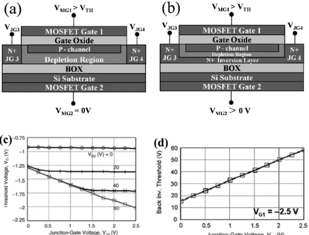
There’s another special four-gate FET, whose gate structure is shown in figure 1-18 (a). It is based on a double-gate FET (with the MOSFET gate 1 and gate 2), while the two junction gates (gate 3 and gate 4) have modulated the threshold voltages of the top gate and the back gate when the double-gate MOSFET is working.
Figure 1-18: The schematic view of four-gate FET (a) with the top gate working, (b) with the
double gate working, (c) the top gate threshold voltage VT1 and (d) the back gate threshold
voltage VT2 modulated by different junction-gate voltages VJG.
Chapter 1 Introduction
22
at off-state and on-state, respectively. When the back-gate is at on-state, the depletion region is narrowed when a back-gate bias VMG2 is applied, and the two gates are coupled. At this state,
the two junction gates (gate 3 and gate 4) could modulate the potential distribution near the junction-gates, thus the threshold voltage VT1 of the top gate 1 and the inversed threshold
voltage VT2 of the back gate 2 could also be modulated, which are shown in figure 1-18 (c)
and figure 1-18 (d), respectively. With the increase of the junction gate voltage VJG= VJG3=VJG4, higher absolute value of VT1 or VT2 is obtained [53].
Note that, even though the alternative 3D structures have been researched to further improve the electrical characteristics, due to the most mature process, the FinFET is still the most popular 3D FET that has been adopted for applications. The advantages of these devices have shown the interest of 3D structure, especially in the better channel controlling in comparison with the planar structure. However, for these 3D devices, the current path is still parallel to the planar surface, which indicates that the channel length is still defined by lithography technque. These 3D devices also demostrate some other drawbacks that need to be solved, especially for the lateral relief of the etched sidewall, which is a general problem for 3D devices. And for our vertical TFTs (VTFTs), it is predictable that this drawback will also be unavoidable introduced.
IV. Vertical transistors: vertical MOSFETs and vertical TFTs
(VTFTs)
IV.1 Introduction of vertical MOSFETs
In many domains such as solar cells [56], ULSI devices [57] and random access memories (RAMs) [58], the prior motivation consists in obtaining a higher current density, which could be realized by reducing the channel length of the devices. As mentioned above, for the previous 3D devices, the channel length is limited by the resolution of the lithography technique. Vertical MOSFET is another type of MOSFET that source and drain are located top and bottom instead of on the same plane, with the channel (gate) vertically located between source and drain, as shown in figure 1-19. Therefore, the channel length of a vertical
Chapter 1 Introduction
23
MOSFET is determined by the thickness of the formed mesa, which is independent of the lithography technique, thus it enables to fabricate an ultra-short channel length.
Figure 1-19: Schematic view of a vertical MOSFET.
Vertical MOSFETs have been widely researched, Lothar Risch et al. have fabricated vertical MOSFETs using Molecular Beam Epitaxy (MBE) layers [59, 60], while J. Moers et al. use a Selective Epitaxial Growth (SEG) method to reduce gate to source/drain capacitances [61, 62]. Haitao Liu et al. have also fabricated a vertical MOSFET with an ultra-thin channel layer to provide a better gate control [63, 64]. In addition, delta doping is adopted by C.Fink group in order to obtain sharp channel profiles and thus better control of electric field [65, 66], while the Steve Hall group use a dielectric pocket as the junction stopper [67, 68].
According to the 3D MOSFETs mentioned above, such as the FinFET, ITFET, GAAFET and so forth, the wrapped gates enable better control of the channel. The 3D vertical MOSFETs are also proposed, known as the gate-all-around (GAA) vertical MOSFET [69].
Figure 1-20 (a) shows the 3D schematic view of the GAA vertical FET, with a wrapped gate around the whole channel. Sometimes, the channels are made up of silicon nanowires (SiNWs), which are well known as the SiNW-based GAA vertical FET [70], shown as the figure 1-20 (b). Just as the GAA planar FET, the GAA vertical FET could ensure the control of the channel part, with a better suppression of the SCEs.
Chapter 1 Introduction
24
Figure 1-20: Schematic view of the 3D Gate-all-around (GAA) vertical MOSFET, (a) the
common GAA vertical FET, and (b) the SiNW-based GAA vertical FET.
IV.2 Introduction of VTFTs
Corresponding to the vertical MOSFETs, the vertical TFTs (VTFTs) have also been developed using thin film technology for over three decades. The VTFT could also be seen as rotating the LTFT 90°. As shown from figure 1-21 (a), for LTFT, source and drain are on the same plane that is parallel to the substrate, and the channel length L is determined by the lithography technique.
Figure 1-21: Schematic view of (a) the N-type LTFT, and (b) the N-type VTFT, the two types
of TFTs are compatible with the classical CMOS technology.
As shown in figure 1-21 (b), VTFT is gained by rotating LTFT 90°, and source and drain are not on the same plane. Therefore, the channel length L could be precisely controlled by the deposition technique (undoped poly-Si thickness), and thus it enables an unltra-short channel length L beyond the resolution limitation of the lithography tools. This short channel length L enables a higher on-current ION, as well as a higher integration density of the devices,
Chapter 1 Introduction
25
(b), due to the etching of the three poly-Si layers’ stacking, it is easier to fabricate a double-gate VTFT, which further doubles the on-current ION. In addition, by narrowing the
width of the etched mesa, the double-gate structure is more efficient in suppressing the short channel effects (SCEs) due to the coupling of the potential distributuon of the two gates.
IV.2.1 Comparison between LTFTs and VTFTs
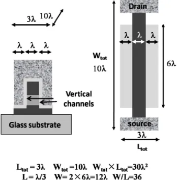
As mentioned above, the vertical structure enables a short channel length L that is determined by the deposition technique instead of the lithography technique, and thus VTFT helps to increase the on-current ION, in comparison with its lateral conterpart. Figure 1-22
shows a schematic cross-sectional view of the LTFT. The device dimension on the glass substrate is evaluted by the design rule λ. As it is shown in figure 1-22, for a LTFT with the minimin device dimension of 30λ2, the device length and width are 15λ and 2λ, respectively, while channel width/length ratio W/L = 2λ/2λ = 1.
Figure 1-22: Schematic cross-sectional view of a LTFT, the device dimension is 15λ×2λ,
while channel width and channel length ratio W/L = 2λ/2λ = 1.
In contrast, for a VTFT with the same device dimension, the channel width and channel length ratio W/L could be much higher. Figure 1-23 shows the cross-sectional view and the top view of a VTFT, whose device length and width are 3λ and 10λ, respectively, which leads to a same device dimension of 30λ2. On one hand, due to the special 3D structure, the device length could be reduced to 3λ. As a result, the channel width W could be 2×6λ = 12λ, considering that there are two channels on the two sidewalls. On the other hand, due to the definition of the channel length L by the deposition technique, the channel length L could be shrinked to λ/3. As a result, the channel width length ratio W/L could be 12λ/(λ/3) = 36. In
Chapter 1 Introduction
26
theory, as the drive current is proportional to W/L, VTFT enables to increase the drive current about 40 times [73]. This increased drive current is the main advantage of VTFT in comparison with LTFT, which is beneficial for large-current applications.
Figure 1-23: Schematic cross-sectional and top view of a VTFT, the device dimension is
3λ×10λ, while channel width and channel length ratio W/L = 12λ/(λ/3) = 36.
IV.2.2 State of the art for VTFTs
VTFT has been researched over two decades. James D. Flummer group has fabricated a VTFT using the anisotropic As+ implanted source/drain, however, the dopant diffuses after a long-time annealing [74]. Tan Fulei et al. have fabricated VTFTs with a self-aligned offset, by adopting the inverted structure. However, the adopted high-temperature (T = 850°C) anneling method is not compatible with the glass substrates, while the Ni-silicide induced lateral crystallization technology (NSILC) involves more complex processes [75]. Tan Fulei et al. have also fabricated a novel VTFT using excimer-laser anneaing (ELA) method to form the active layer, the high-cost method is also a challenge for large-size glass substrate applications [76].
In our research work, another VTFT structure is proposed, with more gates arranged in parallel, as shown in figure 1-24 (a). On one hand, this multi-gate structure enables to further increase the on-current ION, as ION is proportional to the channel width/length ratio W/L.
Chapter 1 Introduction
27
Taking the VTFT in figure 1-22 (a) as an example, there are two teeth for this VTFT, thus there are four gates on the four sidewalls (four parallel channels), then the channel width W is four times of each channel width on the sidewall. In fact, this special 3D structure could enable much more teeth, as long as the tooth width is narrow enough, and this special multi-gate structure is also named “comb-shaped VTFT”. On the other hand, in the fabrication process, for all the thin films deposited in our laboratory, especially for the poly-Si layers deposited by LPCVD technique, the maximum temperature is 600°C, which is compatible with the glass substrates (for example, Corning 1737 glass substrates). The source and drain layers are in situ doped, and no additional diffusion or implantation step is required. Therefore, it facilitates the fabrication process, and the dopant diffusion problem is also avoided. In addition, this multi-gate structure also helps to increase the packing density, which is another advantage of the vertical structure.
Figure 1-24 (b) shows the side view of the multi-gate VTFT, there is a partial etching step at the source side, so that the top and bottom heavily-doped layers could be accessed at the same time. In addition, the large overlap that passes through the undoped poly-Si is also observed.
Chapter 1 Introduction
28
V. Conclusion
The scale-down tendency of the microelectronic devices follows Moore’s law, which proposes higher requirement in the lithography and etching techniques. In addition, the serious short channel effects (SCEs) also degrades the electrical property of the devices. Therefore, new device architecture is necessary to pursue Moore’s law.
The gate engineering of the FETs, especially for the three-dimensional (3D) FETs, has shown its remarkable superiority in channel controlling. The 3D FinFET structure has been adopted in Intel’s 22 nm node CPU technology, which shows a reduced off-current IOFF as
well as a decreased threshold voltage VTH. Other alternative structures have also been
proposed, including inverted T-shaped FET (ITFET), Pi-gate FET, Omega-gate FET, Gate-all-around (GAA) FET, four-gate FET, and so on. The advantages of these devices show the interest of 3D structure, however, they also give evidence of some drawbacks that need to be solved.
Vertical transistor (Vertical MOSFET or VTFT) is obtained by rotating the planar transistor (planar MOSFET or LTFT) 90°, and it could provide several advantages:
1) Channel length is defined by the deposition technique instead of the lithography technique, thus it reduces the technological dependence on lithography;
2) Ultra-short channel FET could be fabricated with a large channel width, which helps to increase the drive current;
3) Higher packing density could be provided in comparison with its lateral counterpart.
A lot of vertical MOSFETs and vertical TFTs (VTFTs) have been researched for more than three decades. In our laboratory, a new multi-gate VTFT is proposed, which further increases the drive current. A low-temperature fabrication process is employed, with the maximum temperature of 600°C, which is compatible with glass substrates.
In chapter 2, this multi-gate VTFT will be introduced in detail. Initially, different techniques in the fabrication process will be given, especially the mature LPCVD and SPC techniques for poly-Si layers deposition will be presented in detail. After that, the fabrication
Chapter 1 Introduction
29
process of the VTFT will be presented step by step, and the first electrical characteristics will be demonstrated. Afterwards, some technological modifications on the structure will be proposed, the obtained electrical characteristics will be further analyzed and discussed in detail.
Chapter 2 Related techniques, process flows, and electrical characteristics of the classical VTFTs
Chapter 2 Related techniques, process flows,
and electrical characteristics of the classical
Chapter 2 Related techniques, process flows, and electrical characteristics of the classical VTFTs
32
In the previous chapter, the basic structure and working principle of the LTFT have been presented, and the VTFT has also been proposed corresponding to the vertical MOSFET, by using thin film technology. In this chapter, we will detailedly describe the fabrication process of the classical VTFT structure, which is fabricated by rotating LTFT 90°. The fabrication process is based on polycrystalline silicon (poly-Si) thin film layers deposited by the low pressure chemical vapor deposition (LPCVD) technique, and the low-temperature (T ≤ 600°C) process enables to be compatible with glass substrates. This chapter initially describes the related materials and techniques adopted in the VTFT fabrication process, which have also been involved in the previous LTFT fabrication process. First, due to their importance in the fabrication of our classical VTFT, silicon layers deposited by LPCVD and annealed by solid phase crystallization (SPC) technique are especially described in detail. Then, other related materials and techniques are also introduced. Afterwards, the fabrication process flow of the classical VTFT with three poly-Si layers’ stacking structure is listed step by step. The key technological challenge for the classical VTFT structure is explained, and devices are electrically characterized and analyzed to highlight the drawbacks of the VTFT structure, for example, the parasitic channel and the large overlapping area. At the end of this chapter, some improvements to solve these problems are also presented.
I. Related materials and techniques in thin film technology
In our laboratory, different thin film materials and deposition methods have been well developed and adopted on different substrates. The mature thin film deposition technologies of semiconductor, insulator, and metallic layers have been involved in the devices and circuits fabrication. The laboratory has great potential and ability in the deposition of thin films by using different techniques, such as LPCVD, plasma-enhanced chemical vapor deposition (PECVD), RF sputtering, thermal evaporation, and so on. Our laboratory also has the know-how in the technological fabrication of devices and circuits in the clean room, as well as the electrical characterization of the devices and circuits.
Chapter 2 Related techniques, process flows, and electrical characteristics of the classical VTFTs
33
I.1 Introduction of different silicon structures: mono-Si, a-Si and poly-Si
Silicon is the basic and fundamental material of the semiconductor industry, because of its interesting electrical properties, as well as its abundance on the earth. Silicon could be divided into three categories according to their different crystal structures: the monocrystalline silicon (mono-Si), amorphous silicon (a-Si), and the intermediate state, which is called polycrystalline silicon (poly-Si).
In mono-Si structure, the Si atoms regularly arrange in a long range order. For an ideal silicon crystal, the atoms arrange as the diamond structure, which follows the face-centered cubic Bravais lattice. The schematic tetrahedral arrangement of the silicon atoms in the diamond structure is shown in figure 2-1. For each bond of adjacent atoms, the interatomic distance is 2.35 Å, and the separation angle is 109°28′ between two bonds.
Figure 2-1: Schematic tetrahedral arrangement of the silicon atoms.
In a crystal, this kind of Si-Si bond induces electronic states, leading to the formation of the energy bands. The atomic distance between two atoms determines the width between the energy bands. The last energy level completely filled with electrons is called valence band (VB), and the next allowed energy level is called conduction band (CB). For Si, the energy gap Eg between the two energy levels is 1.12 eV. This low value enables electrons to easily
transit from VB to CB. Among the three types of Si forms, mono-Si is an ideal semiconductor material that enables to get the best characteristics. However, the production of mono-Si needs the highest economic cost, which requires an extraction step by melting and
Chapter 2 Related techniques, process flows, and electrical characteristics of the classical VTFTs
34 re-solidifying silicon.
The a-Si is the non-crystalline form of silicon. However, it maintains some properties of the crystalline silicon (mono-Si). In fact, the interatomic distance of a-Si keeps at 2.35 Å, while normally every atom is connected with four adjacent atoms. However, for a-Si, the long range order of mono-Si is not present, and the atoms form a continuous random network. Sometimes the fourfold coordinated structure is not strictly followed, and some atoms present dangling bonds. These dangling bonds act as defects in the continuous random network, which act as localized states in the band gap. These localized states trap the carriers and thus modify the transport of the carriers, and thus it is expected that the electrical properties of a-Si seriously degrade in comparison with mono-Si. However, a-Si is much easier to be produced via a low-cost way. In our laboratory, a-Si can be deposited by LPCVD technique or by PECVD method.
Poly-Si is a crystalline structure of silicon that is between mono-Si and a-Si. For poly-Si, the crystal lattices of the whole material is disordered, thus it contains a lot of small silicon crystals (crystallites or grains), with crystalline defects (grain boundaries) between two adjacent crystals. From this point of view, poly-Si can be considered as a combination of mono-Si (grains) and a-Si (grain boundaries), and its properties are determined by the two parts listed below:
- The grain is characterized by its size and its crystalline quality. As poly-Si is a deposited structure, whose grain size cannot be comparable to the one of mono-Si, defects are inevitablely introduced. These defects could be dislocations or macles in the silicon crystals. For the dislocations, they result in the formation of dangling bonds. For the macles, if they end at the surfaces of the grains, they will just divide the grains into more, smaller crystallites. In contrast, if they end in the grains, they would also result in dangling bonds. The defect density determines the grain quality.
- The grain boundary is characterized by its dimension (thickness) as well as its defect density.
Chapter 2 Related techniques, process flows, and electrical characteristics of the classical VTFTs
35
The energy states distribution of poly-Si is shown below in figure 2-2. The band tail due to the disordered arrangement of the crystals, and the deep-level traps caused by dangling bonds, are shown in this figure. These defects degrade the electrical properties of poly-Si in comparison with mono-Si.
Figure 2-2: Schematic model of poly-Si energy states distribution.
Among the three silicon forms, poly-Si is an essential and fundamental material in the fabrication of the TFTs. On one hand, compared with mono-Si, poly-Si is much easier to be compatible with all kinds of substrates, such as glass substrates, plastic substrates and so on; on the other hand, in contrast with a-Si, the better crystalline structure of poly-Si enables to improve the electrical characteristics, especially the field effect mobility. Therefore, poly-Si is in fact more beneficial to be used in the display fields, such as the AMLCD (Active Matrix Liquid Crystal Display) and AMOLED (Active Matrix Organic Light-Emitting Diode). In summary, being the basic material of TFTs, poly-Si compromises the advantages of mono-Si and a-Si, thus it dominates the semiconductor thin film technology.
For poly-Si thin film deposition, the widely-used techniques also include LPCVD and PECVD methods. For PECVD, the plasma of the reacting gas is generated by RF frequency between two electrodes. The energetic plasma dissociates the precursor molecules, and thus the dissociated molecules (such as silicon) are directly deposited on the sample surface, or react with each other to generate new thin film material (such as silicon nitride Si3N4) on the
Chapter 2 Related techniques, process flows, and electrical characteristics of the classical VTFTs
36
sample. PECVD technique allows the deposition of materials at a very low temperature. For example, silicon could be deposited under 300°C by PECVD using silane (SiH4), disilane
(Si2H6), or dichlorosilane (H2SiCl2) as the precursor gases. In fact, in our laboratory, LTFTs
have been fabricated based on the low-temperature PECVD process, including the deposition of silicon by SiH4 (diluted in Argon and hydrogen gases), as well as the deposition of Si3N4 by
SiH4 and Ammonia (NH3) precursor gases (diluted in nitrogen adjunction) [77]. Due to the
low-temperature technique, PECVD leads to deposit poly-Si with a smaller grain size, so-called “microcrystalline silicon”, which degrades the electrical property, especially the drive current and field effect mobility. However, it enables the process to be compatible with flexible substrates, such as plastic substrates, which reveals its potential applications in soft-substrate display field [78, 79].
LPCVD is a widely used technique in microelectronic industry for poly-Si deposition. For LPCVD technique, there are two ways to deposit poly-Si layers. One way is called “as-deposited poly-Si”, which directly deposits poly-Si without a crystallization step. The deposition temperature is usually high to directly crystallize the deposited silicon, while the pressure is low. A typical as-deposited condition could be at the temperature of more than 620°C with the reduced pressure between 120 - 350 mTorr, while the SiH4 gas flow rate is 50
- 200 sccm, and the grain size is around 40 nm [80].
The other way is the deposition of a-Si by LPCVD followed by a crystallization step. The crystallization step could be variable, and in our laboratory, the combination of LPCVD at 550°C and conventional thermal annealing at 600°C is the commonly used method that enables to obtain poly-Si with a large grain size [81]. The conventional thermal annealing is a kind of solid phase crystallization (SPC) technique, and it has been widely used for the fabrication of LTFTs, which have exhibited excellent electrical characteristics, especially for the high field effect mobility [82]. Therefore, for our VTFTs, the poly-Si thin film layers are also obtained by the combination of LPCVD and SPC techniques.