HAL Id: hal-01558568
https://hal.archives-ouvertes.fr/hal-01558568
Submitted on 8 Jul 2017
HAL is a multi-disciplinary open access
archive for the deposit and dissemination of
sci-entific research documents, whether they are
pub-lished or not. The documents may come from
teaching and research institutions in France or
abroad, or from public or private research centers.
L’archive ouverte pluridisciplinaire HAL, est
destinée au dépôt et à la diffusion de documents
scientifiques de niveau recherche, publiés ou non,
émanant des établissements d’enseignement et de
recherche français ou étrangers, des laboratoires
publics ou privés.
10 GBit/s Optical Transmissions at 1.98 µm in cm-long
SiGe Waveguides
Manon Lamy, Christophe Finot, Julien Fatome, Mickael Brun, Pierre Labeye,
Sergio Nicolleti, Adonis Bogris, Dimitris Syvridis, Mohamed Ettabib, David J
Richardson, et al.
To cite this version:
Manon Lamy, Christophe Finot, Julien Fatome, Mickael Brun, Pierre Labeye, et al.. 10 GBit/s
Optical Transmissions at 1.98 µm in cm-long SiGe Waveguides. Electronics Letters, IET, 2017, 53
(17), pp.1213-1214. �10.1049/el.2017.1961�. �hal-01558568�
1
10 GBit/s Optical Transmissions at 1.98
µm in cm-long SiGe Waveguides
M. Lamy, C. Finot, J. Fatome, M. Brun, P. Labeye, S.
Nicolleti, A. Bogris, D. Syvridis, M. A. Ettabib, D. J.
Richardson, P. Petropoulos and K. Hammani
We demonstrate error-free transmission of 10-Gbit/s non-return to zero optical signals along 2.5-cm long SiGe waveguides at a wavelength of 1.98 m. Bit error rate measurements confirm the absence of penalty during the transmission through a subwavelength 1.3 m-wide waveguide as well as through a 2.2 m wide waveguide.
Introduction: Silicon photonics currently attracts much attention as an
emerging technology for on-chip communications and all-optical processing. This interest is even more pronounced with the recent shift toward mid-infrared wavelengths. Indeed, in order to face the continuous and inexorable increase of the data traffic and to avoid the so-called ‘capacity crunch’, attention now focuses on non-conventional spectral regions, including the 2 µm spectral band that can benefit from the emergence of thulium doped fibre amplifiers (TDFA) [1]. This trend has stimulated studies of dedicated photonic components such as InP-based modulators [2], arrayed waveguide gratings or low-loss hollow core bandgap photonic fibers for transmission over hundreds of meters [3, 4]. In the present study, we investigate the performance of Silicon Germanium (SiGe) waveguides. Such components have been thoroughly studied in the C-band [5] where their nonlinear properties have been beneficial for ultrafast optical processing [6]. However, such waveguides are expected to reach even better performance at mid-IR wavelengths. Even though they have been used to convert a signal from mid-IR to C-band [7], no high bit-rate transmission has been reported so far. Here, we demonstrate, for the first time, an error-free transmission of a 10-Gbit/s on-off keying signal at 1.98 µm in 2.5-cm long SiGe waveguides. Two waveguides having different widths are compared.
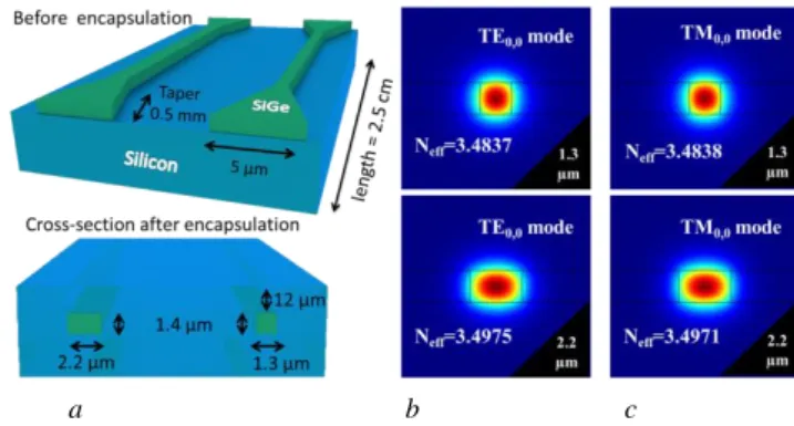
Waveguide design and fabrication: We have designed and fabricated two
optical waveguides sketched in Fig. 1a and made of Si1-xGex grown on a
Si substrate and encapsulated in Si. Both structures have a 1.4-µm height and a length of 2.5 cm but their widths differ. We compare the performances of a subwavelength 1.3-µm wide device and a 2.2-µm wide waveguide. Optical losses in the 2 µm spectral region are expected to be as low as 2 dB/cm, so that propagation through 2.5 cm is fully realistic. The high contrast of optical indexes between SiGe and Si (3.54 and 3.45 respectively, at a wavelength of 1.98 µm [8]) enables excellent confinement of the light within the waveguides (see Fig1b and Fig1c). At the wavelength under study, the 1.3-µm waveguide is bimodal and can handle one TE mode and one TM mode, whereas the 2.2-µm wide waveguide can guide two TE and two TM modes. The TE and TM fundamental modes have almost identical indices. In order to facilitate butt-coupling injection/collection of light to/from the waveguide, 5-µm wide and 500-µm long input and output tapers have been included in the photonic components. The external facets are cleaved at normal incidence.
The fabrication process consists of several epi-layers of Si1-xGex grown
on a Si substrate. First, a 1.4-µm thick SiGe layer with 20% germanium concentration (x = 0.2) was grown by reduced pressure chemical vapor deposition (RP-CVD) to control precisely the Germanium concentration and thus preserve uniformity. Then, standard photolithography and deep reactive ion etching were used to form the strips. Finally, the waveguides were encapsulated with a 12-µm Si cladding layer epitaxially grown with the same RP-CVD technique.
a b c
Fig. 1 Design and fields for 1.3-µm wide (at the top) and 2.2-µm wide (at
the bottom) waveguides.
a Sketches of studied waveguides before encapsulation b Field of the TE fundamental mode for the two waveguides c Field of the TM fundamental mode for the two waveguides
Experimental set-up: In order to demonstrate the suitability of our SiGe
components for high speed optical transmission around 2.0 µm, we have implemented the set-up presented in Fig. 2. The transmitter is based on a laser diode (CW) centred at a wavelength of 1.98 µm and intensity-modulated by means of a lithium-niobate modulator. The transmitted signal is a 231
-1 pseudo-random bit sequence (PRBS) at 10 Gbit/s encoded by a non-return-to-zero on-off-keying modulation format. A polarization controller (PC) is inserted after the intensity modulator so as to mitigate the polarization sensitivity of SiGe waveguides. An optical isolator is also included to protect the active devices from the spurious Fresnel back-reflections that may arise at the component facet due to the large optical index difference between air and Si. Light is injected into the waveguide through butt-coupling taking advantage of optical lensed-fibers.
Two variable optical attenuators (VOA) are inserted into the set-up: the first one is used to control the power injected into the device and thus adjust the optical signal–to-noise ratio (OSNR) at the receiver, whereas the second one preserves a constant power on the photodiode (PD). A power meter and an optical spectrum analyser (OSA) measure the power before and after transmission, respectively. The OSA is also used to evaluate the OSNR of the received signal. The PD can be connected either to a high speed sampling oscilloscope or to a bit error rate tester (BERT) in such a way to monitor the output eye diagrams or perform the bit error rate (BER) measurements, respectively. An optical bandpass filter is inserted into the set-up in order to limit the accumulation of amplified spontaneous noise emission generated from the two TDFAs.
Fig. 2 Experimental set-up for the 10 Gbit/s transmissions at 1.98 µm.
CW: continuous wave ; IM: intensity modulator ; PC: polarization controller ; TDFA: thulium doped fibre amplifier ; OVA: optical variable attenuator ; PM: powermeter; PRBS: pseudo-random bit sequence ; OSA: optical spectrum analyser ; PD: photodiode.
Experimental results at 2 µm:
We have successively tested the subwavelength and the 2.2 µm wide waveguides for optical data transmissions. Total fiber-to-fiber losses close to 33 dB and 30 dB have been measured respectively, for polarized CW light at 1.98 µm. Note that our goal here was not to optimize the optical coupling (the tapers that are present are identical and have not been optimized for each waveguide width individually). We have noted
2
experimentally that given its design accepting both TE and TM modes with similar efficiency, the subwavelength waveguide was only marginally polarisation dependant.
The eye diagrams shown in Fig.3 offer us an initial overview of the quality of the 10 Gbit/s transmissions. The eye diagrams after propagation are well open both for the subwavelength and for the 2.2 µm wide waveguides and do not exhibit significant degradations compared to the back-to-back measurements.
a b
Fig. 3 Eye diagrams for 1.3 µm wide SiGe waveguide (top) and 2.2 µm
wide SiGe waveguide (bottom). a Back-to-back configuration
b After transmission through the waveguides
To further evaluate the quality of the high-speed optical transmissions at 1.98 µm, BER measurements have been carried out for the two devices. Error free transmissions (BER ≤ 10-12) at 1.98 µm wavelength have been achieved through both 2.5-cm long SiGe waveguides of two different widths. Quantitative measurements of the influence of the OSNR on the output BER are summarized in Fig.4. For each structure, BER measurements after transmission through the waveguide are compared with the result obtained in back-to-back configuration (to this aim, a variable optical attenuator with equivalent losses to the device is used replacing the structure and the two lensed-fibers). As can be seen, results are very similar and propagation through the photonic component does not induce any power penalty. Furthermore, the bimodal or multimodal properties of the waveguides do not seem to impact the transmission quality. Given the input power injected into the waveguide (peak power of 150 mW are typically coupled to the waveguides), the various nonlinear effects that may exist in Si or SiGe material and that are used in the context of optical processing do not impair the propagation. To support this argument, we have checked the output spectrum and found it rather identical to the input one.
a b
Fig. 4 BER as a function of OSNR for 2.5-cm long SiGe waveguides. The
black circles are associated with the back-to-back configuration while red crosses indicate BER measurements at the output of the waveguides. The red line corresponds to the associated linear regression.
a Graph for the 1.3-µm wide SiGe waveguide. b Graph for the 2.2-µm wide SiGe waveguide
Conclusion: We have demonstrated error free transmission of 10 Gbit/s
optical signals in SiGe 2.5-cm long waveguides at the wavelength of 1.98 µm. No significant penalty has been recorded on the BER measurements after transmission into a subwavelength waveguide and through waveguide having a width of 2.2 µm. These results pave the way for the
use of SiGe-based components for high-repetition rate transmissions combined with simultaneous nonlinear processing in the near-infrared region.
Acknowledgments: This work was supported by the European Union
within the Seventh Framework Programme FP7/2007-2013 under Grant 288304 (STREP CLARITY) and within the framework of the operational Program FEDER-FSE Bourgogne 2014/2020. It was also supported by the Région Bourgogne (Pari Photcom) and by Carnot Arts Institute (PICASSO 2.0 project).
M. Lamy, C. Finot, J. Fatome and K. Hammani (Laboratoire
Interdisciplinaire Carnot de Bourgogne (ICB), UMR 6303 CNRS – Université de Bourgogne Franche-Comté, 9 Avenue Alain Savary, BP 47870, 21078 Dijon Cedex, France)
E-mail: kamal.hammani@u-bourgogne.fr
M. Brun, P. Labeye and S. Nicolleti (CEA-Leti MINATEC Campus, 17
rue des Martyrs 38054 Grenoble Cedex 9, France)
A. Bogris and D. Syvridis (Department of Informatics and
Telecommunications, National and Kapodistrian University of Athens, Panepistimiopolis, Ilissia, 15784, Athens, Greece)
M. A. Ettabib, D. J. Richardson and P. Petropoulos (Optoelectronics
Research Centre, University of Southampton, Highfield, Southampton, SO17 IBJ, UK)
A. Bogris: also with Department of Informatics, Technological Educational Institute of Athens, 12210 Egaleo, Athens, Greece
References
1. Soref, R., 'Group Iv Photonics: Enabling 2 µM Communications',
Nature Photon., 2015, 9, (6), pp. 358-359.
2. Ye, N., Gleeson, M.R., Sadiq, M.U., Roycroft, B., Robert, C., Yang, H., Zhang, H., Morrissey, P.E., Suibhne, N.M., Thomas, K., Gocalinska, A., Pelucchi, E., Phelan, R., Kelly, B., O’Carroll, J., Peters, F.H., Gunning, F.C.G., and Corbett, B., 'Inp-Based Active and Passive Components for Communication Systems at 2 µM', J. Lightwave
Technol., 2015, 33, (5), pp. 971-975.
3. Xu, K., Sun, L., Xie, Y., Song, Q., Du, J., and He, Z., 'Transmission of Im/Dd Signals at 2 µM Wavelength Using Pam and Cap', IEEE
Photonics J., 2016, 8, (5), pp. 1-7.
4. Petrovich, M.N., Poletti, F., Wooler, J.P., Heidt, A.M., Baddela, N.K., Li, Z., Gray, D.R., Slavík, R., Parmigiani, F., Wheeler, N.V., Hayes, J.R., Numkam, E., Grűner-Nielsen, L., Pálsdóttir, B., Phelan, R., Kelly, B., O’Carroll, J., Becker, M., MacSuibhne, N., Zhao, J., Gunning, F.C.G., Ellis, A.D., Petropoulos, P., Alam, S.U., and Richardson, D.J., 'Demonstration of Amplified Data Transmission at 2 µM in a Low-Loss Wide Bandwidth Hollow Core Photonic Bandgap Fiber', Opt. Express, 2013, 21, (23), pp. 28559-28569.
5. Hammani, K., Ettabib, M.A., Bogris, A., Kapsalis, A., Syvridis, D., Brun, M., Labeye, P., Nicoletti, S., Richardson, D.J., and Petropoulos, P.,
'Optical Properties of Silicon Germanium Waveguides at
Telecommunication Wavelengths', Opt. Express, 2013, 21, (14), pp. 16690-16701.
6. Ettabib, M.A., Kapsalis, A., Bogris, A., Parmigiani, F., Rancaño, V.J.F., Bottrill, K., Brun, M., Labeye, P., Nicoletti, S., Hammani, K., Syvridis, D., Richardson, D.J., and Petropoulos, P., 'Polarization Insensitive Wavelength Conversion in a Low-Birefringence Sige Waveguide', IEEE Photon. Technol. Lett., 2016, 28, (11), pp. 1221-1224. 7. Hammani, K., Ettabib, M.A., Bogris, A., Kapsalis, A., Syvridis, D., Brun, M., Labeye, P., Nicoletti, S., and Petropoulos, P., 'Towards Nonlinear Conversion from Mid- to near-Infrared Wavelengths Using Silicon Germanium Waveguides', Opt. Express, 2014, 22, (8), pp. 9667-9674.
8. Humlíček, J., Röseler, A., Zettler, T., Kekoua, M.G., and Khoutsishvili, E.V., 'Infrared Refractive Index of Germanium–Silicon Alloy Crystals', Appl. Opt., 1992, 31, (1), pp. 90-94.