HAL Id: hal-03047502
https://hal.archives-ouvertes.fr/hal-03047502
Submitted on 15 Dec 2020
HAL is a multi-disciplinary open access archive for the deposit and dissemination of sci-entific research documents, whether they are pub-lished or not. The documents may come from teaching and research institutions in France or abroad, or from public or private research centers.
L’archive ouverte pluridisciplinaire HAL, est destinée au dépôt et à la diffusion de documents scientifiques de niveau recherche, publiés ou non, émanant des établissements d’enseignement et de recherche français ou étrangers, des laboratoires publics ou privés.
Effect of AlGaN interlayer on the
GaN/InGaN/GaN/AlGaN multi-quantum wells
structural properties toward red light emission
Pierre Ruterana, Magali Morales, Nicolas Chery, Thi Ngo, Marie-Pierre
Chauvat, Kaddour Lekhal, Benjamin Damilano, Bernard Gil
To cite this version:
Pierre Ruterana, Magali Morales, Nicolas Chery, Thi Ngo, Marie-Pierre Chauvat, et al.. Effect of AlGaN interlayer on the GaN/InGaN/GaN/AlGaN multi-quantum wells structural properties toward red light emission. Journal of Applied Physics, American Institute of Physics, 2020, 128, pp.223102. �10.1063/5.0027119�. �hal-03047502�
Effect of AlGaN interlayer on the GaN/InGaN/GaN/AlGaN
multi-quantum wells structural properties towards red light emission.
Pierre Ruterana1, Magali Morales1,a), Nicolas Chery1, Thi Huong Ngo2,3, Marie-Pierre Chauvat1,
Kaddour Lekhal2, Benjamin Damilano2,and B. Gil3 AFFILIATIONS
1CIMAP, UMR 6252, CNRS, ENSICAEN, Université de Caen-Normandie, CEA, 6
Boulevard du Maréchal Juin 14000 Caen, France
2Université Côte d’Azur, CNRS, CRHEA, Rue Bernard Gregory, 06560 Valbonne, France 3 L2C, CNRS and Univ. Montpellier, case courrier 074, 34095 Montpellier CEDEX 5, France
a)Author to whom correspondence should be addressed: magali.morales@ensicaen.fr
ABSTRACT
In this work, InGaN/GaN Multi-Quantum Wells (MQWs) with strain compensating AlGaN interlayers grown by metalorganic vapour phase epitaxy have been investigated by high resolution X-ray diffraction, transmission electron microscopy and photoluminescence (PL). For different AlGaN strain compensating layer thicknesses varying from 0 to 10.6 nm, a detailed X-ray diffraction analysis shows that the MQW stack become completely strained on GaN along a and c. The compensation is full from an AlGaN layer thickness of 5.2 nm, and this does not change up to the largest one that has been investigated. In this instance, the AlGaN was grown at the same temperature as the GaN barrier, on top of a protective 3 nm GaN. It is found that the crystalline quality of the system is progressively degraded when the thickness of the AlGaN interlayer is increased through strain concentrated domains which randomly form inside the 3 nm GaN low temperature layer. These domains systematically contribute to a local decrease of the QW thickness and most probably to an efficient localisation of carriers. Despite these defects, the PL is highly improved towards the red wavelengths and compares with the reports on ultrathin AlGaN layers where this has been correlated to the improvement of the crystalline quality although with less strain compensation.
This is the author’s peer reviewed, accepted manuscript. However, the online version of record will be different from this version once it has been copyedited and typeset.
I. INTRODUCTION
InGaN/GaN QWs heterostructures have already proven theirs efficiencies in blue Light Emitting Diodes (LED).1 For larger wavelengths, due to the increased indium composition
needed, the compressive strain on the InGaN QWs is relaxed by generation of defects such as stacking faults,2,3 inversion domains4,5 and dislocations6,7 which may contribute to a fast degradation of the optical performance. Therefore the successful fabrication of efficient emitters in the green wavelengths range and beyond critically depends on the possibility to growth good quality material,8 and in addition to find ways of managing the Quantum Confined Stark Effect (QCSE) which is inherent to the polarity along the [0001] direction in wurtzite structure.9 Indeed, avoiding the latter effect through the growth along non-polar orientation has allowed demonstration of green lasers.10 However, the growth on non-polar or semi-polar orientations would need to incorporate more indium than along the polar orientation in order to attain a similar emission wavelength. This may lead to layers degradation through the formation of defects, and the trade-off seems to still be at the advantage of using polar substrates.8 Along this vein, it was reported that the use of ultrathin layers (UL) of AlGaN (1-2 nm) deposited at the same temperature (755°C) as the InGaN well may help for the development InGaN/AlGaN/GaN based LED with high indium content in the QW.11
The AlGaN UL seems to have at least three roles: (i) such a UL deposited at low temperature might lead to improve the crystalline quality of the heterostructure.12 (ii) It also
helps to attain a higher indium incorporation up to 25 %.13 However, the strain compensation
of such ULs is limited, for the investigated thicknesses (≤ 2.1 Å), a nearly pseudomorphic growth was only obtained for the Al0.4Ga0.6N at a UL thickness of 1 Å where the measured
lattice parameter is closest to that of GaN.14 Interestingly, this thickness of 1 Å corresponds to
the highest photoluminescence intensity as well as smallest peak width.14 (iii) Finally, such
UL may help to improve the external quantum efficiency for red light emission.12
Earlier, it was reported that the use of AlxGa1-xN (x = 0.2) layers of thickness up to 10 nm,
grown at the top of the GaN barrier may also help to improve the yellow/amber light emission of InGaN QWs and this was attributed mostly to a better crystalline quality of the MQWs due to the strain reduction.15 Further investigations showed that these heterostructures also exhibited good quantum efficiency.16 In this work, our aim is to report on a detailed structural investigation of these heterostructures using High Resolution X-ray Diffraction (HRXRD)
This is the author’s peer reviewed, accepted manuscript. However, the online version of record will be different from this version once it has been copyedited and typeset.
and Transmission Electron Microscopy (TEM) techniques in order to try to shine some light on the dominant mechanisms that may govern the improved light emission in these systems.
II. EXPERIMENTAL
The heterostructures were grown along the [0001] direction by metalorganic vapour-phase epitaxy on GaN/Al2O3 substrates (Fig. 1). In our samples, the protection for the InGaN was
insured by growing a 3 nm GaN layer at the same temperature (715°C) before increasing to 940°C for the growth of the Al0.2Ga 0.8N and top GaN layers. The total thickness of this
barrier (GaN (3 nm)/AlGaN/GaN) was kept to around 17 nm when varying the Al0.2Ga0.8N
thickness from 0 to 10.7 nm (samples S1 to S4), and the top AlGaN/GaN was slightly n-doped (Si: 51018 cm-3) with the aim to optimize the emission performance.17
FIG. 1. Schematics of the investigated MQW stack.
The QW and barrier system were repeated 10 times (Fig. 1). In the first four samples S1 to S4, the InGaN QWs have a nominal indium composition of 21% whereas in the last sample S5, the InGaN QWs In content is 23%. The nominal characteristics of the samples are summarized in Table I where xIn is the indium composition of the InGaN QWs, LInGaN and
LAl0.2Ga0.8N are the widths of the InGaN and AlGaN layers, respectively. LGaN-tot is the total
thickness of GaN inside the barrier; it includes the low temperature 3 nm, grown on top of InGaN at the same temperature.
TABLE I. The nominal characteristics of the samples
Reciprocal Space Maps (RSM) have been recorded using a high resolution Philips X’Pert MRD four circles diffractometer or a Rigaku Smartlab Cu high-resolution X-ray diffractometer with a 2 bounce Ge (220) single crystal (Cu1 = 1.54056 Å radiation) and 9 kW rotating anode generator. RSM around the symmetric (0002) and non-symmetric (101̅4)
Samples xIn LInGaN (nm) LAlGaN (nm) LGaN-tot (nm)
S1 0.21 2.6 0 15.2
S2 0.21 2.6 1.4 15.6
S3 0.21 2.6 5.2 11.9
S4 0.21 2.6 10.6 7.0
S5 0.23 2.6 5.2 11.9
This is the author’s peer reviewed, accepted manuscript. However, the online version of record will be different from this version once it has been copyedited and typeset.
Bragg reflections were used respectively to determine the mean c out-off plane and a in-plane lattice constants of the MQW stack according to references.18-20 In order to verify if in plane
local relaxation is present in our samples, a direct measurement around the (101̅0) GaN diffraction peak has been also performed.21
The surface morphology of all the samples was investigated by Atomic Force Microscopy (AFM). For TEM analysis, cross sections (thickness around 80 nm) were prepared by Focused Ion Beam (FIB) FEI-660-NanoLab by decreasing energies (30 kV to 1 kV) and currents down to few pA in order to minimise the damage. Conventional TEM was carried out in a JEOL 2010 microscope equipped with a LaB6 filament and High Resolution Scanning
Transmission Electron Microscopy (HRSTEM) was performed in a double corrected JEOL-ARM200F.
Photoluminescence (PL) measurements of these samples at 8K and 300K were carried out using a third harmonic of a femtosecond Ti: sapphire laser with a fundamental wavelength of 800 nm, a pulse width of 100 fs and a repetition rate of 82 MHz crosses a Tripler TP-2000B system to form a laser beam with a wavelength of 266 nm. Then, it was focused on the samples by a lens down to spot of about 14 µm. The emission signal coming from the samples was detected by a back-illuminated CCD camera (Andor Newton 920).16
III. RESULTS
A. OPTICAL PROPERTIES
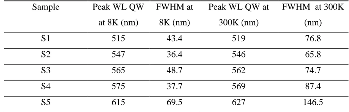
Before discussing the results of the structural investigation, we start by presenting the PL measurements on these samples. To this end, the emission at 8K and 300K (Fig. 2) is exhibited along with the corresponding width of the peaks (Table II). At low temperature (8K), as soon as the AlGaN interlayer is introduced, we have a large effect for the red shift (32 nm) and a consistent intensity increase in S1 and S2. At a thickness of 5.2 nm, when the measured in-plane and c parameters are expected to coincide with those of GaN, the shift is smaller (18 nm) and the emitted intensity does not increase (S3). When the AlGaN layer is 10.6 nm thick, the redshift is only 10 nm, but the intensity increase is largest (S4).
FIG. 2. Low (8K) and room temperature PL of samples S1 to S5
Comparing S3 and S5, which have the same nominal AlGaN interlayer thickness, the red shift is largest (50 nm) and the gain in intensity is consistent. However, S5 PL peak is asymmetric; it has additional contributions on the high-energy side in contrast to the four
This is the author’s peer reviewed, accepted manuscript. However, the online version of record will be different from this version once it has been copyedited and typeset.
other samples. At room temperature, one can compare only S2-S4, among these samples, the corresponding PL peaks are symmetric, and the emitted intensity increases with the AlGaN interlayer thickness. However, as can be seen, the FWHM steadily increases from S2 to S4 whereas the redshift is now only 23 nm.
TABLE II. Photoluminescence at low (8K) and room temperatures for the 5 samples Sample Peak WL QW at 8K (nm) FWHM at 8K (nm) Peak WL QW at 300K (nm) FWHM at 300K (nm) S1 515 43.4 519 76.8 S2 547 36.4 546 65.8 S3 565 48.7 562 74.7 S4 575 37.7 569 87.4 S5 615 69.5 627 146.5
At room temperature, the situation is more complex for S5 and S1; the PL signal from sample S5 markedly decreases, it has a highly non-symmetric shape and it is not accurate to determine the maximum emission wavelength and the peak width. In sample S1, two PL peaks are clearly present with the green maximum at 519 eV and the smaller peak at 459 in the blue range. Interestingly, as discussed in reference 16, the internal quantum efficiency increases from S1 to S4, we go from 50 to 57% at 8K, and from 2.3 to 4.3% at room temperature. Therefore, we have a clear improvement in the optical properties as brought about by the inserted the Al0.2Ga0.8N interlayers and this correlates with the increase of their
thickness. In the case of the Al rich 1 nm thick UL, it was proposed that they help to improve the crystalline quality of the system by protecting the QW during the temperature ramp up, also leading to a possible increase of indium incorporation.11-14 In our samples, the question is what are the mechanisms that govern this improvement?
B. STRUCTURAL ANALYSIS
The AFM image in Fig. 3(a) shows that the sample S1, which does not include any AlGaN inside the barrier, exhibits a surface morphology with usual atomic steps, characteristic of a two dimensional growth, interrupted by a quite low density of dislocation emerging at the layer surface, in the form of pinholes. Their density may be correlated with that of the
This is the author’s peer reviewed, accepted manuscript. However, the online version of record will be different from this version once it has been copyedited and typeset.
threading dislocations from the GaN template.12 In samples S2 to S3 (Fig. 3(b) and 3(c)), with
the AlGaN thickness increase, more pinholes form and the surface morphology is increasingly modified. Moving to the largest AlGaN thickness sample S4, the surface exhibits not only pinholes, that are large, but additional features have formed which are similar to trenches as already reported in the literature.22
FIG. 3. Surface morphology of the sample S1 (a), S2 (b), S3 (c), S4 (d) and S5 (e).
As can be seen, there are also larger features which are similar to the trench defects reported to form with densities in the range from 1x107 cm-2 to 5x108 cm-2 on top of multiple InxGa 1-xN (2.5 nm) QWs (x10) deposited at 725-740 °C along with a 1 nm GaN protection UL before
ramping up in to 860°C for the deposition of the GaN barrier (7.5 nm), in this instance, the indium composition x was in the 0.17-0.2 range.22 Sample S5 exhibits the same surface morphology as sample S4 but with the In content increase we observe a larger surface degradation. In the (0002) RSM of sample S1 (Fig. 4(a)), two contributions have been evidenced with a main sharp peak coming from the (0002) reflection of the GaN template and a second highest peak at lower angle relative to that of the GaN which is the zero-order peak (SL0) of AlGaN/InGaN/GaN superlattice fringes.
FIG. 4. (0002) XRD symmetric RSM of samples S1 (a) and S4; (b); (101̅4) XRD asymmetric RSM of the sample S1 (c) and S4 (d). The sample S5 (not shown here) exhibits identical (0002) and (101̅4) XRD RSM to those of sample S4.
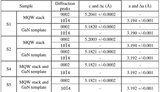
With the AlGaN thickness increase, the SL0 peak gets closer to the GaN template peak and for samples S4 (Fig. 4(c)) and S5 (not shown here) the two peaks are merged. The corresponding extracted mean c lattice constants (Table III), are an average of two (InGaN/GaN) and three (AlGaN/InGaN/GaN) different layers in the MQW stack of samples S1 and S2 to S5, respectively. For sample S1, in the (101̅4) RSM we observe a very small but detectable difference (at around 10-4 RLU) between the lateral positions of the
AlGaN/InGaN/GaN MQW stack fringes and the GaN template peaks corresponding to MQW stack strain relaxation. For samples S3 to S5 (Fig. 4(d)), in the (101̅4) RSM, the GaN and AlGaN/InGaN/GaN MQW stack reflections are vertically aligned showing that these heterostructures are fully strained. Moreover, in the (101̅4) RSM of samples S1 to S4 (Fig 4(c) and 4(d)), with the AlGaN layer thickness increase; we observed a vertical shift of the main SL0 peak of the MQW stack towards that of the GaN template.
This is the author’s peer reviewed, accepted manuscript. However, the online version of record will be different from this version once it has been copyedited and typeset.
TABLE III. Mean c and a lattice constants of GaN template and AlGaN/InGaN/GaN MQW stack, the corresponding measurement errors are also given (c and a).
Sample Diffraction
peaks c and ∆c (Å) a and ∆a (Å)
S1 MQW stack 0002 5.2041 +/-0.0002 - 101̅4 - 3.194 +/-0.001 GaN template 0002 5.1820 +/-0.0002 - 101̅4 - 3.190 +/-0.001 S2 MQW stack 0002 5.2003 +/-0.0002 - 101̅4 - 3.194 +/-0.001 GaN template 0002 5.1821 +/-0.0002 - 101̅4 - 3.192 +/-0.001 S4 MQW stack and GaN template 0002 5.1821 +/-0.0002 - 101̅4 - 3.192 +/-0.001 S5 MQW stack and GaN template 0002 5.1821 +/-0.0002 - 101̅4 - 3.192 +/-0.001
Therefore, the mean a parameters of AlGaN/InGaN/GaN MQW stack progressively settle to that of the GaN template (Table III). If we now compare these a values with the theoretical ones obtained by minimizing the elastic strain energy (equilibrium lattice a parameters of 3.199Å, 3.197 Å, 3.194 Å, and 3.189 Å for samples S1 to S4),15 we observe small differences
which go beyond the error bars from HRXRD measurements as displayed in Table III. This may be an indication of the presence of misfit dislocations at heterointerfaces, as previously reported in GaN/AlN MQW heterostructures.23
In our samples, with the AlGaN thickness increase, the mean c and a lattice parameters of the MQW stack changes; consequently, the average perpendicular and parallel elastic strain changes can be due to those in the AlGaN/InGaN/GaN MQW stack composition (In content and/or Al content) and/or thicknesses. As the HRXRD observed in-plane strain can be the result of local c parameter changes in the different layers of the MQW stack, we further carried out TEM analysis. As we have a repetition of ten AlGaN/GaN/InGaN/GaN MQWs, plan-view observations are rather complex, so in the following only cross section geometry will be discussed. Taking into account the possible defects, which form in the wurtzite structure i.e. the 3 dislocations (a, c, a+c) and the corresponding partials dislocations, basal (I1, I2, E)3 and prismatic stacking faults.24 In the investigated samples, no contrast of such typical defects can be seen using g=0002. In Fig. 5, we display the images of all the samples (S1 Fig. 5(a) to S5 Fig. 5(e)); the surface has been marked by a short white arrow. Apart from
This is the author’s peer reviewed, accepted manuscript. However, the online version of record will be different from this version once it has been copyedited and typeset.
the fringes which correspond to thickness changes, some threading dislocations (TD) are visible; moreover, towards the surface, additional features can be seen in these weak beam images as marked with small inclined arrows. Their density is highly increased from sample S1, where only one such feature is present seen in the displayed area, to S5 (Fig. 5(e)) in which the surface area is filled with a variety of these defects.
Many of them exhibit a small white contrast, which is elongated in the basal plane, and some are connected to the surface. From the above micrographs recorded using g=101̅0, and as we do not have any contrast using g=0002, the observed defects have only components inside the basal planes, they can be either 1/3 <112̅0> dislocations or 1/3<101̅0> type stacking faults. In order to determine what they exactly correspond to, let’s focus on the surface area of sample S5 where they are found at highest density as can be seen in Fig. 5(e).
FIG. 5. A cross section weak beam micrograph with g=011̅0 for the samples S1 (a), S2 (b), S3 (c), S4 (d), S5 (e). Some TDs and small defects (arrows) in the surface area are marked.
Fig. 6 corresponds to such an area at a higher magnification. In the g=0002 weak beam image (Fig. 6(a)), except the a+c mixed type threading dislocation (TD) which is visible for the 4 used imaging conditions, the defects that form inside the quantum area are all out of contrast. In this weak beam image, as the different layers are imaged edge on, the quantum wells are now markedly visible (see short white arrows limiting the area) although with quite poor resolution.
It is thus clear that the features of interest have been generated inside the area (Fig. 5(b)-(d)). There are three such features as marked in Fig. 6(b), which is a week beam image recorded with g= 011̅0 close to the [21̅1̅0] zone axis; in this figure, the contrast is quite broad, but it is clear that feature 3 which is large inside the basal plane forms a closed domain. In a next step, the sample was tilted by 30° around [0001] to the [101̅0] zone axis in order to record the weak beam image of Fig. 6(c) with g=12̅10 where all the a type dislocations are in contrast. As can be seen, the domain features are now out of contrast, but some linear features () are visible inside the basal plane; they could be either segments of a type screw dislocations or most probably partial dislocations of <101̅0> type as they are not in contrast all around the domains.
FIG. 6. Weak beam images of the surface area of sample S5, (a) g=0002; (b) g=011̅0 close to the [21̅1̅0] (c) g=112̅0 close to the [101̅0] zone axis and (d) with g=[011̅0] close to the [42̅2̅3]
This is the author’s peer reviewed, accepted manuscript. However, the online version of record will be different from this version once it has been copyedited and typeset.
From feature 1, three a type dislocations have been generated and they thread up to the layer surface (Fig. 6(c)), two segments are also visible in the basal plane (). In order to confirm the domain structure, we further tilted the sample in order to have a larger projected area in the corresponding images. To this end, the sample was tilted by 39° around the [011̅0] towards the [42̅2̅3] zone axis and we recorded the corresponding weak beam image (Fig. 6(d)). As can be seen, the domain features exhibit fringes which are characteristic of planar defects with, of course, a displacement vectors parallel to <101̅0> directions; they form domains which are limited by six {21̅1̅0} facets. The subsequent point was to determine how theses defects relate to the InGaN quantum wells, so we carried out scanning transmission TEM (STEM), along with EDS.
A typical annular dark field (ADF) image of the quantum well area in S4 is exhibited in Fig. 7. It was recorded with a camera length of 20 cm in our ARM200; this condition allows revealing mostly the strain contrast as shown by the 10 QWs which come out in form of brightest areas. In this image where a threading dislocation (TD) can be seen, three domains (1, 2, 3) are present at the level of QWs 3 and 4 from the surface. Domain 1 has a type dislocations (D) that propagate to the surface where a step is visible at their emergence point (white inclined arrow) in agreement with the AFM observations (Fig. 3(c)). The domains are not exactly inside the QWs, they formed on top. Also, as underlined by the two horizontal white arrows, the composition in the AlGaN layer may not be uniform; in this sample, this dark strip towards the surface contains around 39% Al as determined by EDS.
FIG 7. ADF image of the quantum well area in sample S4, three domains (1,2,3), and QWs thickness fluctuations (black arrows) are visible
The other point to underline is that, for the 10 QWs, the thickness is not uniform as may be suggested by to the nominal value of 2.6 nm as given in Fig. 1. We clearly see thickness change from one QW to the other, and thickness variation in all the quantum wells (see black inclined arrows). The connection of the domains and the QW is better seen through observations at higher magnification (Fig. 8).
FIG 8. High magnification STEM images of the domain 1 area in Fig. 7, (a) ADF at a camera length of 20 cm, (b) High Angle ADF image at a camera length of 6 cm.
This is the author’s peer reviewed, accepted manuscript. However, the online version of record will be different from this version once it has been copyedited and typeset.
Indeed, the domain sits at the top of the quantum well and the threading dislocation seems to emerge from its upper part (Fig. 8(a)) comparing with Fig. 8(b), which displays mostly a chemical contrast, it can be seen that the domain is located inside the top GaN barrier. In this particular domain, the quantum well thickness is almost reduced to zero towards the left end of the domain. This is the same for domain 3 in Fig. 6, but as can be seen, domain 2 sits on a uniform but slightly decreased thickness of the QW. It also should be underlined that our structures are highly complex, the composition of the AlGaN interlayer is not uniform along the growth direction, the white arrows point to dark areas where the Al concentration is increased in Fig. 8(b). In the most Al rich horizontal strips, the Aluminium content can be as high as 40% as determined by EDS measurements (for instance in the strip marked by the two white horizontal arrows in Fig. 6). However in all these samples, we hardly approach the nominal value of 20%, out of those random areas where the concentration is highest, the Al concentration measured by EDS is rather around 10-12%. The situation is not simple either for the indium distribution, which is not easy to measure by EDS, as the QW thickness varies with a three dimensional geometry as is easily deduced from the ADF two-dimensional projections. By acquiring more than 20 points in uniform thickness areas (as QW1 of Fig. 8), we also find that the indium composition changes from point to point. In the measurements that were carried out, we find for instance that the In fluctuation amplitudes can be as high as, for instance from 15 to 23% in S1, 15 to 30% in S3, 19 to 23% in S4 and 10 to 28% in S5. Of course, the largest amplitudes come from different quantum wells; for each sample, the spectra were recorded using the same acquisition conditions. Concerning the defect domains, as mentioned above, we can see them in images recorded with a large camera length (20 cm), as they are located inside the GaN barrier, they should contain small amount of indium, if any. Fig. 8(a) shows a high-resolution ADF image of such a domain (black arrows) with an emerging dislocation (D) in sample S3. Locally, the thickness of the QW is only about 1 nm and goes to zero towards the right, under the dislocation. The measured thickness of the domain is 4.6 along the c-axis, which, when added to the 1 nm of the QW makes 5.6 nm. This corresponds to the nominal thickness of the QW and barrier as expected from the used growth conditions (see Fig. 1). In Fig. 9(b), we can see the EDS spectrum as acquired at the probe position shown by the inclined white arrow in Fig. 9(a). As expected from the image contrast, there is no indium and the only elements detected from the sample are gallium and nitrogen.
FIG. 9. EDS analysis of a domain in sample S3, (a) ADF image showing the domain (black arrows) and the probe position during the data acquisition (white arrow). The contrast of the
This is the author’s peer reviewed, accepted manuscript. However, the online version of record will be different from this version once it has been copyedited and typeset.
dislocation (D) emanating from the domain is clearly visible. (b) The corresponding acquired EDS spectrum where no indium is present. The probe position is shown by the arrow.
Therefore, these domain defects are formed by a random local accumulation of the strain on top of the QW with possible displacement vectors along <101̅0>. The strain comes from the indium composition inside the QWs and/or from the AlGaN interlayer thickness; their density is seen to increase with both.
It should be interesting to know how and when these domains build up during the growth of the heterostructures. What is clear for now is that they form inside the GaN barrier, just on top of the QWs. They are limited by six hexagonal facets of {21̅1̅0} type and they contain a very small concentration of indium if any (not showing up in EDS). When they form, the quantum well geometry is modified; its thickness is systematically decreased, and in most cases, it even can shrink to zero at one edge of the domain, mostly when a dislocations have been generated and emerge to the surface. At these nominal indium compositions around 20%, as seen in Fig. 7, even without the formation of defect domains, the thickness of the QWs is not uniform, and as determine by EDS, neither is the composition.
IV. DISCUSSION
Previously, the attempts to bridge the green gap using AlGaN UL for strain management have proposed that UL should be very thin (1nm) and be Al rich ( > 40%).11-14
With their MQW structure of 3 nm InGaN QW, 1 nm AlGaN UL (Al=90%), and a 10 nm InGaN barrier, Huang et al.12 reported an EQE of 2.9% at 629 nm and room temperature with a FWHM of 53 nm, an injection current of 20 mA and a DC power of 1.1 W. In this instance, the QW and the AlGaN UL were grown at 755°C and the barrier GaN was grown at 100°C higher; the In content of the QW were estimated to 35%. The optical performance was the correlated to an improved crystalline quality with no other V defects at the surface except those from the GaN template dislocations.12 However, the theoretical proposal25 modelled such ULs at the aluminium composition of 20%, and 1 nm thickness for strain compensation. The systems were MQWs with In-content ranging up to 28%, corresponding to active regions around 500 nm wavelength for LED applications. In this case, the In.28Ga.72N QW (strain:
+3.13%) was 24 Å thick with the 1 nm Al.2Ga.8N (strain=-0.17%). This theoretical work
motivated our detailed investigation from the growth of the samples and optical investigations15,16 to this microstructural study. In reference 25, it was proposed that the tensile AlGaN barriers led to the improvement of the material quality, and to the enhancement
This is the author’s peer reviewed, accepted manuscript. However, the online version of record will be different from this version once it has been copyedited and typeset.
of the electron–hole wave functions overlap. In addition, the larger conduction and valence band offsets provided by the AlGaN ULs lead to more confinement of the carriers in the QW. As can be seen in Fig. 10, the tensile strain introduced by the 1nm AlGaN (Fig. 10(a)) UL is small and will not compensate the difference between GaN and InGaN (Fig. 10(b)), even when the Al composition is 90% especially for an (In=35 %) InGaN QW (strain: +4.57%) as mentioned in references 11 and 12.
FIG 10. The strain contribution of the various layers as related to GaN, for uniformity, the strain is determined using the results of reference 26; (a) InGaN and (b) AlGaN alloys, respectively.
Therefore, we investigated larger thicknesses of the AlGaN interlayer and used a different geometry growing the quantum well and a 3nm GaN layer at the same temperature and the AlGaN as well as the rest of the GaN barrier some 100°C higher. As seen above from HRXRD, the MQW stack becomes completely strained to GaN, only starting at 5.2 nm Al0.2Ga0.8N thickness, where the a and c lattice parameters do not change any more.
Interestingly, the optical properties continue to improve until the AlGaN thickness of 10.6 nm. However, as shown already by the AFM and confirmed by TEM, the behaviour of our stack is completely different from those which consisted in the 1 nm Al rich ones deposited directly at the same temperature as the InGaN quantum well followed by the higher temperature growth of the GaN barriers.11-14 Consequently, the improvement of the optical
properties in our samples does not coincide with that of the structural quality.
Obviously, the geometry of our systems is different from those where the growth of the AlGaN UL took place directly on top of the QW. In our layers, this TEM investigation shows In fluctuations, QW width and Al content variations; this certainly result on local lattice parameters changes inside the InGaN or AlGaN layers of the MQW stack. These changes are more important for sample S4, exhibiting the largest AlGaN thickness, and in S5 with the largest nominal In content (23%). However, it is worth noticing that in the corresponding in-plane grazing incidence diffraction measurement at around (101̅0) GaN template, for all samples, neither broadening nor splitting of the peak can be visualized and this has been attributed to a local partial strain relaxation.20 Therefore, both the increase of the AlGaN thickness and the MQW stack local composition variations are sources of partial strain relaxation in these heterostructures leading to the observed structural degradation. So this local strain relaxation takes place in different ways without the conventional formation of misfit dislocations as the QWs are below the critical thickness for plastic relaxation in the
This is the author’s peer reviewed, accepted manuscript. However, the online version of record will be different from this version once it has been copyedited and typeset.
InGaN/system.27 Starting with S1 with no AlGaN interlayer and 2.65 % strain in the a
direction, we already have the formation of the small domain defects, as seen above, their density strongly increases with the AlGaN thickness and the indium concentration. They form on top of the QWs, and finally generate a type threading dislocations that propagate towards the sample surface. Rather interesting, the presence of these domains is observed to be simultaneous with the decrease of QW thickness and even its local disappearance.
In earlier investigations of defects interaction with InGaN/GaN MQW the focus has been put mostly on the V-defects may due to the opening of mainly a+c dislocations when crossing the QWs,28 or even by basal stacking faults that transform to prismatic ones29 inside the MQW area.30 Indeed, as can be seen in the AFM images, we have a multiplication of V-defects up to formation of trenches22 when the AlGaN is thickest and eve more when the indium nominal concentration is increased to 23% (see Fig. 2 (d) and 2 (e)). However, the domain defects that we observe in these samples may be better interpreted in the light of some recent reports.3,31,32 They are only generated in the quantum well area and are not connected to any threading dislocation from the underlying GaN template. One domain can be at the origin of more than two threading dislocation the thread to the layer surface and terminate as small V-defects. In reference 31, the authors reported pairs of inclined dislocation that generated inside the QW area on top of self-supported substrates with low dislocation density; however the possible origin of such defects was not clearly determined. A quite similar case as in our observations was reported in reference 32, where each defect in the basal plane could be at the origin of numerous a type dislocations. These dislocations were shown to randomly form around the InGaN/GaN or QWs area of low indium content 7-15%, and it was proposed that they were due to the dissociation of 1/3 <101̅0> I2 (Schockley) stacking faults. If now we consider that the formation of the stacking faults is the dominant mechanism to generate these defects, we should also take into account of the geometries and energetics. In the wurtzite system, there are mainly 3 stacking faults (I1, I2, E) corresponding to the three dislocations of the hexagonal lattice (a, c, a+c). From the geometry, the first stacking mistake with the insertion of only 1 cubic sequence would lead to the formation of the I1 (1/3 <202̅3>) stacking fault, as the Shockley I2 introduces two cubic sequences in the wurtzite stacking, in agreement with the energetic calculations.33 With the E (1/2 [0001]) stacking fault characterized by 3 cubic sequences, the three stacking faults display their sequences in [112̅0] zone axis high resolution TEM images and they all form, for instance in the low temperature nitride buffer layers.3 More recently, it was reported that the source of these a-type dislocations from domains in InGaN/GaN layers and QWs could be exclusively due to I1 SFs
This is the author’s peer reviewed, accepted manuscript. However, the online version of record will be different from this version once it has been copyedited and typeset.
which should be organized in way so that they can dissociate into a threading dislocations and a new type of stacking fault named I4 was proposed to explain their formation mechanism.34
In the above reports, the position and relationship between these defect domains and the QWs has not been clearly established. In this report, we focus on the role of the AlGaN interlayers, however, our current investigations attempt to determine the strain relaxation mechanisms InGaN/GaN QWs with the aim to address the green gap issue. To this end, we consider indium composition from 15% to above 20% with the emission going until red-yellow wavelengths. From our observations, with the improvement of the growth techniques, the three dimensional growth with deep V-defects30 can be eliminated, and the remaining issue is probably the internal strain relaxation, which, we think, is at the origin of the formation of these domains. In fact, they start to form at low indium concentrations, and this corresponds to the observations reported by Meng et al.32 In the early stages the domains are of various size and mainly small and no stacking fault contrast effect can be seen in HRTEM images on the wurtzite sequence, see Fig. 5(a) in reference 32. It would be interesting to see if the formation of these domains depends on the growth kinetics. As seen above, they strongly interact with the growth of our QWs, reducing to almost and even zero their thickness. Most probably, in our used growth procedure, where the AlGaN interlayer was deposited at the usual GaN barrier temperature, the dynamics is completely different from what has been reported in references 11-14, where the 4 monolayer AlN rich layer could play a more protective role than our low temperature 3nm GaN.
If now we consider the notable improvement of the room temperature luminescence with the increased AlGaN thickness, the domains may play an indirect role. As observed above, they highly contribute to the generation of the inclined a threading dislocations which are known to be detrimental to the optical properties of the QWs as locations of non-radiative recombination.32 Interestingly, they locate on the top of the wells; at their apex, the well
thickness gradually drops to zero, and they are confined inside that the 3nm GaN low temperature ultrathin layer. Moreover, their formation does not involve any indium redistribution with escape from the QW. Indeed, there is no measurable amount of indium inside (see Fig. 9). So they probably result from a dynamical distribution of the local strain. For the moment, our work is going on to try to understand the mechanisms that may govern the formation of these domains. If now we consider the notable improvement of the luminescence with the increased AlGaN thickness, clearly this is not due to the crystalline quality of the layers. Maybe, the geometry of our QWs, which takes the form of lenses due the strain redistribution due to the formation of these defects, could be compared with what
This is the author’s peer reviewed, accepted manuscript. However, the online version of record will be different from this version once it has been copyedited and typeset.
has been called gross well width fluctuation34 for the emission at green wavelengths in
InGaN/GaN quantum wells. However, at this point, it is difficult to give a definitive explanation of our PL results from the above defect analysis alone. In order to draw a final conclusion, on-going combined optical studies are on the way to systematically determine the influence of these defects.
V. CONCLUSION
In summary, heterostructures of In0.21-0.23Ga0.79-0.77N/GaN MQWs with different thicknesses
of Al0.2Ga0.8N interlayers were investigated. The emission of these heterostructures is
improved with the increase of AlGaN barriers thicknesses and for a given Al0.2Ga0.8N
interlayer thickness with an In content increase at around 21%. HRXRD measurements showed that the MQW stacks become completely strained along a and c on GaN with the AlGaN thickness. By AFM and TEM investigations, we observed a degradation of the crystalline quality and an increase of defects density with the AlGaN interlayer thickness. In contrast to previous reports where Al rich ultrathin layers (~1 nm) were deposited on the InGaN QW at the same temperature before the growth of the barrier, the protection layer was made of a low temperature 3nm GaN layer. Within this kinetically different situation, a clear improvement of the PL emission is obtained towards the red wavelengths. We observe new defects that are in the form of hexagonal domains which form inside the 30 nm GaN layer on top of the InGaN QWs without any incorporation of indium. These defects contributed to a systematic local reduction of the QW thickness, which probably increases the localisation of the charge carriers inside wells and may decreases the non radiative effect of the generated a type dislocations. Therefore, it may be forecast that if this growth is well controlled, such a process may help to improve the layers structural quality towards red light emission of InGaN/GaN quantum wells.
ACKNOWLEDGMENTS
This work was carried out in the scope of the LABEX GANEX, and equally financially supported by the “Région Normandie” through the “FEDER” system, under convention N°15P03533. The LABEX GANEX is funded by the ANR under “Investissements d’avenir” national Programme. Part of the TEM samples were prepared using a FIB facility which has been acquired through the EQUIPEX GENESIS ANR-11-EQPX-0020 within the
This is the author’s peer reviewed, accepted manuscript. However, the online version of record will be different from this version once it has been copyedited and typeset.
“Investissements d’avenir” national Programme with the contribution of the Region Normandie through the FEDER system . The authors want also to thank P. Roussel (UCCS, Lille) for his help in the grazing incidence XRD in-plane measurements.
DATA AVAILABILITY
The data that support the findings of this study are available from the corresponding author upon reasonable request.
REFERENCES
1. S. Nakamura, The roles of structural imperfections in InGaN-Based Blue Light-Emitting
Diodes and Laser Diodes, Science 281, 956 (1998).
2. P. Ruterana, B. Barbaray, A. Béré, P. Vermaut, A. Hairie, E. Paumier, and G. Nouet, A.
Salvador, A. Botchkarev, and H. Morkoc, Formation and stability of the {11-20} stacking fault in wurtzite nitride semiconductors, Phys. Rev. B 59, 15917-15925 (1999).
3. V. Potin, P. Ruterana and G. Nouet, HREM study of stacking faults in GaN layers grown on
sapphire substrate, J. Phys. Condensed Matter 12, 10301 (2000).
4. V. Potin, G. Nouet, and P. Ruterana, The {101̅0} inversion domains in GaN/sapphire
layers: an electron microscopy analysis of the atomic structure of the boundaries, Phil. Mag. A 79, 2899 (1998).
5. M. Zhu , Shi You, T. Detchprohm, T. Paskova, E. A. Preble, D. Hanser, and C. Wetzel,
Inclined dislocation-pair relaxation mechanism in homoepitaxial green GaInN/GaN light-emitting diodes, Phys. Rev. B 81, 125325 (2010).
6. V. Potin, P. Ruterana, G. Nouet, R.C. Pond, and H. Morkoç, Mosaic growth of GaN on
(0001) sapphire : a high resolution electron microscopy and crystallographic study of dislocations from low angle to high angle grain boundaries, Phys. Rev. B 61, 5587 (2000).
7. P. Ruterana, V. Potin, B. Barbaray, and G. Nouet, Growth defects in GaN layers on top of
(0001) sapphire: a geometrical analysis of the misfit effect, Phil. Mag. A 80,937 (2000).
8. A. Avramescu, T. Lermer, J. Müller, C. Eichler, G. Bruederl, M. Sabathil, S. Lutgen, and
Uwe Strauss, True green laser diodes at 524 nm with 50 mW continuous wave output power on c-plane GaN, Applied Physics Express 3, 061003 (2010).
9. S. Li, H. Lei, Yi Wang, Md Barkat Ullah, J. Chen, V. Avrutin,U. Özgür, H. Morkoç, and P.
Ruterana, Polarity control within one monolayer at ZnO/GaN Heterointerface:(0001) plane inversion domain boundary, ACS Appl. Mater. Interfaces, 10, 37651 (2018).
10. M. Adachi, InGaN based green laser diodes on semipolar GaN substrate, Jpn J. Appl.
Phys. 53, 100207 (2014).
This is the author’s peer reviewed, accepted manuscript. However, the online version of record will be different from this version once it has been copyedited and typeset.
11. T. Shioda, H. Yoshida, K. Tachibana, N. Sugiyama, and S. Nunoue, Enhanced light output
power of green LEDs employing AlGaN interlayer in InGaN/GaN MQW structure on sapphire (0001) substrate Phys. Status Solidi A 209, 473 (2012).
12. J.I. Hwang, R. Hashimoto, S. Saito, and S. Nunoue, Development of InGaN-based red
LED grown on (0001) polar surface, Applied Physics Express 7, 071003 (2014).
13. D.D. Koleske, A.J. Fischer, B.N. Bryant, P.G. Kotula, J.J. Wierer, On the increased
efficiency in InGaN-based multiple quantum wells emitting at 530–590 nm with AlGaN interlayers, J. Cryst. Growth 415, 57 (2015).
14. S. A. Al Muyeed, W. Sun, X. Wei, R. Song, D. D. Koleske, N. Tansu, and J. J. Wierer,
Strain compensation in InGaN-based multiple quantum wells using AlGaN Interlayers, AIP Advances 7, 105312 (2017).
15. K. Lekhal, B. Damilano, H. T. Ngo, D. Rosales, P. De Mierry, S. Hussain, P. Vennegues,
and B. Gil, Strain-compensated (Ga,In)N/(Al,Ga)N/GaN multiple quantum wells for improved yellow/amber light emission, Appl. Phys. Lett. 106, 142101 (2015).
16. T. H. Ngo, B. Gil, P. Valvin, B. Damilano, K. Lekhal, and P. De Mierry, Yellow–red
emission from (Ga,In)N heterostructures, Internal quantum efficiency in yellow- amber light emitting AlGaN-InGaN-GaN heterostructures, Appl. Phys. Lett. 107, 122103 (2015).
17. P. A. Grudowski, C. J. Eiting, J. Park, B. S. Shelton, and D. J. H. Lambert, Properties of
InGaN quantum-well heterostructures grown on sapphire by metalorganic chemical vapor deposition, Appl. Phys. Lett. 71, 1537 (1997).
18. A. Krost, and J. Bläsing, Evaluation of strain and In content in (InGaN/GaN) multiquantum
wells by x-ray analysis, Appl. Phys. Lett. 75, 689 (1999).
19. M. E. Vickers, M. J. Kappers, and T. M. Smeeton, Determination of the indium content
and layer thicknesses in InGaN/GaN quantum wells by x-ray scattering, Journal of Applied Physics 94, 1565 (2003).
20. R. Ley, L. Chan, P. Shapturenka, M. Wong, S. DenBaars, and M. Gordon, Strain relaxation
of InGaN/GaN multi-quantum well light emitters via nanopatterning, Optics Express 27, 30081 (2019).
21. S. Neugebauer, S. Metzner, J. Bläsing, F. Bertram, A. Dadgar, J. Christen, and A.
Strittmatter, Polarization engineering of c ‐plane InGaN quantum wells by pulsed‐flow growth of AlInGaN barriers, Phys. Status Solidi B 253, No. 1, 118 (2016).
22. F. C. P. Massabuau, M. J. Davies, F. Oehler, S. K. Pamenter, E. J. Thrush, M. J. Kappers,
A. Kovács, T. Williams, M. A. Hopkins, C. J. Humphreys, P. Dawson, R. E. Dunin-Borkowski, J. Etheridge, D. W. E. Allsopp, and R. A. Oliver, Morphological, structural, and emission characterization of trench defects in InGaN/GaN quantum well structures, Applied Physics Letters 101, 212107 (2012).
23. P. K. Kandaswamy, F. Guillot, E. Bellet-Amalric, E. Monroy, L. Nevou, M. Tchernycheva,
A. Michon, F. H. Julien, E. Baumann, F. R. Giorgetta, D. Hofstetter, T. Remmele, M. Albrecht, S. Birner, and Le Si Dang, GaN/AlN short-period superlattices for intersubband
This is the author’s peer reviewed, accepted manuscript. However, the online version of record will be different from this version once it has been copyedited and typeset.
optoelectronics: A systematic study of their epitaxial growth, design, and performance, J. Appl. Phys. 104, 093501 (2008).
24. P. Vermaut, G. Nouet, P. Ruterana, Observation of two atomic configurations for the
{112̅0} stacking fault in wurtzite (Ga, Al) nitrides, Appl. Phys. Lett. 74, 694 (1999).
25. H. Zhao, R. A. Arif, Y. K. Ee, and N. Tansu, Self-Consistent Analysis of Strain
Compensated InGaN–AlGaN quantum wells for lasers and light-emitting diode, IEEE J. Quant. Elec. 45, 66 (2009).
26. Z. Dridi, B. Bouhafs and P. Ruterana, First-principles investigation of lattice constants and
bowing parameters in wurtzite AlxGa1-xN, InxGa1-xN and InxAl1-xN alloys, Semicond. Sci. Tech. 18, 850 (2003).
27. M. Layer, J. Stellmach, C. Meissner, M. Pristovsek and M. Kneissl, The critical thickness
of InGaN on (0001) GaN, J. Cryst. Growth 310, 4913 (2008).
28. X. H. Wu, C. R. Elsass, A. Abare, M. Mack, S. Keller, P. M. Petroff, S. P. DenBaars, and
J. S. Speck, Structural origin of V-defects and correlation with localized excitonic centers in InGaN/GaN multiple quantum wells, Appl. Phys. Lett., 72, 692 (1998).
29. P. Vermaut, P. Ruterana and G. Nouet, Polarity of epitaxial layers and {112̅0} prismatic
defects in GaN and AIN grown on the (0001)Si surface of 6H-SiC, Phil. Mag. A 76, 1215
(1997).
30. H. K. Cho, J. Y. Lee, G. M. Yang, and C. S. Kim, Formation mechanism of V defects in
the InGaN/GaN multiple quantum wells grown on GaN layers with low threading dislocation density, Appl. Phys. Lett. 79, 215 (2001).
31. M. Zhu, S. You, T. Detchprohm, T. Paskova, E. A. Preble, D. Hanser, and C. Wetzel,
Inclined dislocation-pair relaxation mechanism in homoepitaxial green GaInN/GaN light-emitting diodes, Phys. Rev. B 81, 125325 (2010).
32. F. Y. Meng, H. McFelea, R. Datta, U. Chowdhury, C. Werkhoven, C. Arena, and S.
Mahajan, Origin of predominantly a type dislocations in InGaN layers and wells grown on (0001)GaN, J. Appl. Phys. 110, 073503 (2011).
33. C. Stampfl and C. G. Van de Walle, Energetics and electronic structure of stacking faults in
AlN, GaN, and InN, Phys. Rev. B57 (R15 052), 57 (1998).
34. J. Smalc-Koziorowska, C. Bazioti, M. Albrecht, and G. P. Dimitrakopulos, Stacking fault
domains as sources of a-type threading dislocations in III-nitride heterostructures, Appl. Phys. Lett. 108, 051901 (2016).
This is the author’s peer reviewed, accepted manuscript. However, the online version of record will be different from this version once it has been copyedited and typeset.
This is the author’s peer reviewed, accepted manuscript. However, the online version of record will be different from this version once it has been copyedited and typeset.
This is the author’s peer reviewed, accepted manuscript. However, the online version of record will be different from this version once it has been copyedited and typeset.
This is the author’s peer reviewed, accepted manuscript. However, the online version of record will be different from this version once it has been copyedited and typeset.
This is the author’s peer reviewed, accepted manuscript. However, the online version of record will be different from this version once it has been copyedited and typeset.
This is the author’s peer reviewed, accepted manuscript. However, the online version of record will be different from this version once it has been copyedited and typeset.
This is the author’s peer reviewed, accepted manuscript. However, the online version of record will be different from this version once it has been copyedited and typeset.
This is the author’s peer reviewed, accepted manuscript. However, the online version of record will be different from this version once it has been copyedited and typeset.
This is the author’s peer reviewed, accepted manuscript. However, the online version of record will be different from this version once it has been copyedited and typeset.
This is the author’s peer reviewed, accepted manuscript. However, the online version of record will be different from this version once it has been copyedited and typeset.
This is the author’s peer reviewed, accepted manuscript. However, the online version of record will be different from this version once it has been copyedited and typeset.
This is the author’s peer reviewed, accepted manuscript. However, the online version of record will be different from this version once it has been copyedited and typeset.
This is the author’s peer reviewed, accepted manuscript. However, the online version of record will be different from this version once it has been copyedited and typeset.
This is the author’s peer reviewed, accepted manuscript. However, the online version of record will be different from this version once it has been copyedited and typeset.
This is the author’s peer reviewed, accepted manuscript. However, the online version of record will be different from this version once it has been copyedited and typeset.