HAL Id: hal-02120551
https://hal.archives-ouvertes.fr/hal-02120551
Submitted on 6 May 2019HAL is a multi-disciplinary open access
archive for the deposit and dissemination of sci-entific research documents, whether they are pub-lished or not. The documents may come from teaching and research institutions in France or abroad, or from public or private research centers.
L’archive ouverte pluridisciplinaire HAL, est destinée au dépôt et à la diffusion de documents scientifiques de niveau recherche, publiés ou non, émanant des établissements d’enseignement et de recherche français ou étrangers, des laboratoires publics ou privés.
Stable a-Si:H Based Multijunction Solar Cells with
Guidance from Real Time Optics Annual Report, Phase
I
C Wronski, R. Collins, L Jiao, A Ferlauto, P. Rovira, R Koval, Z Lu, X Niu
To cite this version:
C Wronski, R. Collins, L Jiao, A Ferlauto, P. Rovira, et al.. Stable a-Si:H Based Multijunction Solar Cells with Guidance from Real Time Optics Annual Report, Phase I. [Research Report] National Renewable Energy Laboratory. 2000. �hal-02120551�
August 2000 • NREL/SR-520-28809
C.R. Wronski, R.W. Collins, L. Jiao, A. Ferlauto,
P.I. Rovira, R.J. Koval, Z. Lu, and X. Niu
Center for Thin Film Devices
University Park, Pennsylvania
Stable a-Si:H Based
Multijunction Solar Cells
with Guidance from
Real Time Optics
Annual Report, Phase I
17 July 1998–16 October 1999
National Renewable Energy Laboratory
1617 Cole Boulevard
August 2000 • NREL/SR-520-28809
Stable a-Si:H Based
Multijunction Solar Cells
with Guidance from
Real Time Optics
Annual Report, Phase I
17 July 1998–16 October 1999
C.R. Wronski, R.W. Collins, L. Jiao, A. Ferlauto,
P.I. Rovira, R.J. Koval, Z. Lu, and X. Niu
Center for Thin Film Devices
University Park, Pennsylvania
NREL Technical Monitor: B. von Roedern
Prepared under Subcontract No. XAF-8-17619-22
National Renewable Energy Laboratory
1617 Cole Boulevard
Golden, Colorado 80401-3393
NOTICE
This report was prepared as an account of work sponsored by an agency of the United States government. Neither the United States government nor any agency thereof, nor any of their employees, makes any warranty, express or implied, or assumes any legal liability or responsibility for the accuracy, completeness, or usefulness of any information, apparatus, product, or process disclosed, or represents that its use would not infringe privately owned rights. Reference herein to any specific commercial product, process, or service by trade name, trademark, manufacturer, or otherwise does not necessarily constitute or imply its endorsement, recommendation, or favoring by the United States government or any agency thereof. The views and opinions of authors expressed herein do not necessarily state or reflect those of the United States government or any agency thereof.
Available electronically at http://www.doe.gov/bridge
Available for a processing fee to U.S. Department of Energy and its contractors, in paper, from:
U.S. Department of Energy
Office of Scientific and Technical Information P.O. Box 62
Oak Ridge, TN 37831-0062 phone: 865.576.8401 fax: 865.576.5728
email: reports@adonis.osti.gov Available for sale to the public, in paper, from:
U.S. Department of Commerce
National Technical Information Service 5285 Port Royal Road
Springfield, VA 22161 phone: 800.553.6847 fax: 703.605.6900
email: orders@ntis.fedworld.gov
EXECUTIVE SUMMARY
TASK I: Novel Improved Intrinsic Materials for Multijunction Solar Cells
I.1. Novel i-Layers for Solar Cells
Phase diagrams that characterize plasma-enhanced chemical vapor deposition of Si thin films at low substrate temperature (200°C) have been established using real time spectroscopic ellipsometry as a probe of thin film microstructural evolution and optical properties. These deposition phase diagrams describe the regimes over which predominantly amorphous and microcrystalline Si phases are obtained as a function of the accumulated film thickness and the hydrogen-to-silane gas flow ratio R=[H2]/[SiH4]. The diagrams for different substrate materials demonstrate how general principles can be formulated and verified for the design of optimized multistep i-layer components of amorphous silicon p-i-n and n-i-p solar cells.
I.2. Evaluation of Optoelectronic Properties
Research has continued on improving a-Si:H materials for solar cells, particularly with respect to their stability against light-induced degradation. The diluted and undiluted a-Si:H materials that have been studied and characterized were deposited under a wide range of deposition conditions. They have included a-Si:H films from Penn State and Super Laboratory at ETL, as well as our team partners BP Solarex and Uni-Solar. The similarities and differences in their properties have been evaluated and detailed analysis, required for obtaining reliable gap state parameters for all gap states, has been carried out on several of these materials.
Our characterization and analysis results show that in the annealed state, charged defects can dominate the properties of truly “device quality” a-Si:H materials, materials that have actually proven their quality in high performance solar cells. We found that because of the low densities of neutral dangling bond, Do, states in such materials even small changes in charged defects can result in significant difference in the electron mobility-lifetime (µτ) products and
subgap absorption α(hν). If they are interpreted in the simple manner based on Do state dominance, then there are clear inconsistencies between results on subgap absorption and those on µτ products. However the results can be understood when account is taken of the charged defect states. On the other hand, analysis of these charged defects presents a big challenge because their densities cannot be independently measured as in the case of neutral dangling bond defect states, as well as they introduce a large number of new parameters for characterization. The methodology for the characterization of all the gap states, developed at Penn State has been applied to the analysis of results on a-Si:H in materials in both annealed and 1 sun degraded states.
It should also be pointed out that “operational parameters” are not unique because of the flexibility offered in fitting as a result of having as many as 20 different parameters. Nevertheless the ability to obtain good fits to so many results using such “operational parameters” is in direct contrast to the inability to do so when charged defects are not included. It offers some new insights about the nature of gap states and their contribution to solar cell performance and stability.
TASK II: Insights into Improved Stability in Materials and Solar Cells
II.1. Degradation Studies
The type, nature and densities of different light induced defects in optimized a-Si:H materials have been investigated and characterized. These studies have been carried out on films and corresponding Schottky barrier cell structures with different thicknesses of the intrinsic bulk layers. Taking into account the inadequacy of the approach based on solely “neutral dangling bonds”, the characterization was expanded in the attempt to include all of the gap states. We find that light-induced charged defects are as important as the neutral dangling bond defects in determining the properties and stability of a-Si:H materials and solar cells. We also find that
unlike previous claims in truly “device quality” materials the degraded steady states do depend on both intensity and temperature (even less than 70oC). This makes the commonly used
arbitrary, accelerated degradation results meaningless unless they are related to 1 sun degraded states. Extensive studies of light induced defects were carried out on diluted (R=10) Schottky barrier solar cell structures and the corresponding films. The measurements on Schottky barrier cell structures, which include forward I-V, light I-V and QE with different i layer thicknesses, are analyzed with results of µτ products and subgap absorption spectra obtained on the corresponding films. The focus of the work here is mainly on the degraded steady state (DSS) obtained with 1 sun illumination at 25°C in films and Schottky barrier cells. All these results were analyzed using a distribution of gap states shown in Fig.1, where in addition to the neutral dangling bond D0 states two Gaussian distributions of defect states are introduced above and
below midgap. This and the procedure for obtaining “operational” parameters for these states are discussed.
TASK III: Optimization of Solar Cell Performance with Improved Intrinsic
Layers
III.1. Optimization of p/i Interfaces
The formation of p/i interfaces in hydrogenated amorphous silicon p-i-n solar cells prepared by plasma-enhanced chemical vapor deposition has been analyzed in detail using real time optics. With this capability, three effects have been successfully separated and quantified: (i) contaminant layer deposition at the p-layer surface with a sensitivity of ±0.1 Å, (ii) thermal emission of bonded hydrogen from the p-layer with a sensitivity of ±0.1 at.% (± 2 meV in optical gap), and (iii) surface temperature variations with a sensitivity of ±1°C. The separation of these
competing effects has yielded a better understanding of p/i interface formation and has led to an optimum process for device fabrication.
III.2. p-Layers for n-i-p Solar Cells
Real time optical analysis (RTSE) has been applied to study the nucleation, coalescence, and growth processes for ~100-200 Å thick microcrystalline silicon (µc-Si:H) p-layers on H2
plasma-treated amorphous silicon (a-Si:H) i-layers in the substrate/(n-i-p) device configuration. For such i-layers, p-layer microcrystal nucleation at low plasma power is controlled by the catalytic effects of B-containing radicals at the i-layer surface, irrespective of the dopant source, whereas nucleation at higher plasma power is controlled by the bombardment of the i-layer by Si-containing ions. Under high power plasma conditions using BF3, dense single-phase µc-Si:H p-layers can be obtained over a wide range of the dopant gas flow ratio. In contrast, for B2H6 and B(CH3)3, such properties are obtained only over narrow flow ratio ranges owing to the relative ease of dissociation of these gases in the plasma. Based on these results, an optimized µc-Si:H p-layer has been developed for application in n-i-p solar cells.
III.3. Protocrystalline Intrinsic Layers
Studies have been carried out on the thickness dependent transition between the amorphous and microcrystalline phases in intrinsic Si:H materials (i-layers) and its effect on p-i-n solar cell performap-i-nce. P(a-SiC:H)-i(a-Si:H)-p-i-n(µcSi:H) cell structures were deposited with the intrinsic Si:H layer thickness and the flow ratio of hydrogen to silane, R=[H2]/[SiH4], guided by
an evolutionary phase diagram obtained from real-time spectroscopic ellipsometry. The thickness range over which the fill factors are controlled by the bulk was established and their characteristics investigated with different protocrystalline i-layer materials (i.e., materials prepared near the amorphous to microcrystalline boundary but on the amorphous side). Insights into the properties of these materials and the effects of the transition to the microcrystalline phase were obtained from the systematic changes in the initial fill factors, their light-induced
changes, and their degraded steady states for cells with i-layers of different thickness and H2
dilution.
TASK IV: Optimization of Multijunction Solar Cells
IV.1. Textured TCO Studies
We have applied a rotating-compensator multichannel ellipsometer to perform real time Stokes vector spectroscopy (also called polarimetry) during the preparation of hydrogenated amorphous silicon (a-Si:H) p-i-n solar cells on Asahi U-type textured tin-oxide (SnO2) surfaces. With this spectroscopy (1.5 to 4.0 eV), the irradiance Ir and polarization parameters {(Q, χ), p} of the specularly reflected beam are obtained with 0.8 s resolution versus time during solar cell preparation. Here Q and χ are the tilt and ellipticity angles of the polarization state and p is the degree of polarization. An analysis of Q and χ that neglects the effects of the texture can provide the time evolution of the thicknesses, microscopic structure, and the optical properties of the component layers of the a-Si:H solar cell. Deviations of the measured reflectance spectra from those predicted on the basis of the (Q, χ) analysis provide the thickness dependence of the scattering and the evolution of the macroscopic structure of the solar cell. The measurement and analysis approach is important because of its potential application for real time monitoring of solar cell production. The analysis results also provide realistic inputs for optical modeling of the effects of texture in light trapping.
IV.2. Optical Modeling
Analytical expressions have been developed that provide close fits to the dielectric functions ε of amorphous (a), nanocrystalline (nc), and microcrystalline (µc) silicon-based films. These expressions provide the capability of accurate optical modeling of the intrinsic (i) layers used in a-Si:H-based multijunction solar cells. As a result, a set of optical functions
representative of high-density a-Si:H and its alloys spanning the full solar spectrum can be generated from the optical gap alone.
IV.3. Tunnel Junction Formation
Tunnel junction formation for applications in amorphous silicon (a-Si:H) based multijunction n-i-p solar cells has been studied using real time optics. The junction structure investigated in detail here consists of a thin (~100 Å) layer of n-type microcrystalline silicon (µc-Si:H) on top of an equally thin p-type µc-Si:H layer, the latter deposited on thick (~2000 Å) intrinsic a-Si:H. Such structures have been optimized to obtain single-phase µc-Si:H with a high crystallite packing density and large grain size for both layers of the tunnel junction. We have determined the conditions under which grain growth is continuous across the p/n junction and the conditions under which renucleation of n-layer grains can be ensured at the junction. One important finding of this study is that the optimum conditions for single-phase, high-density µc-Si:H n-layers are different depending on whether the substrate is a µc-µc-Si:H p-layer or is a H2-plasma treated or untreated a-Si:H i-layer. Thus, the top-most µc-Si:H layer of the tunnel junction must be optimized in the multi-junction device configuration, rather than in single cell configurations on i-layers. These observations are explained using evolutionary phase diagrams for Si film growth.
TABLE OF CONTENTS
TASK I: Novel Improved Intrinsic Materials for Multijunction Solar Cells... 10
I.1. Novel i-Layer Materials for Solar Cells... 10
Motivation and Overview... 10
Experimental Details... 11
Results and Discussion... 12
Concluding Remarks... 17
References... 18
I.2. Evaluation of Optoelectronic Properties... 29
Results and Discussion... 29
References... 31
TASK II: Insights into Improved Stability in Materials and Solar Cells... 36
II.1. Degradation Studies... 36
Results and Discussion... 36
References... 41
TASK III: Optimization of Solar Cell Performance with Improved Intrinsic Layers... 49
III.1. Optimization of p/i Interfaces... 49
Motivation and Overview... 49
Experimental Details... 49
Results and Discussion... 50
Concluding Remarks... 54
References... 55
III.2. p-Layers for n-i-p Solar Cells... 61
Motivation and Overview... 61
Experimental Procedures... 62
Results and Discussion: Effect of H2-Dilution on the Nucleation and Growth of µc-Si:H p-Layers... 63
Results and Discussion: Effect of Doping Level on the Nucleation and Growth of µc-Si:H p-Layers... 64
Results and Discussion: Effect of Plasma Power on the Nucleation and Growth of µc-Si:H p-Layers... 68
Concluding Remarks... 71
References... 72
III.3. Protocrystalline Intrinsic Layers... 89
Motivation and Overview... 89
Experimental Procedures... 90
Results and Discussion... 91
Concluding Remarks... 94
References... 95
TASK IV: Optimization of Multijunction Solar Cells... 103
IV.1 Textured TCO Studies... 103
Motivation and Overview... 103
Experimental Procedures... 104
Concluding Remarks... 109
References... 110
IV.2. Optical Modeling... 121
Motivation and Overview... 121
Experimental Details... 121
Results... 123
Discussion... 124
Concluding Remarks... 124
References... 125
IV.3. Tunnel Junction Formation... 128
Motivation and Overview... 128
Experimental Details... 128 Results... 130 Discussion... 132 Summary... 133 References... 134 APPENDIX I... 143 Bibliography (1998-1999)... 153
TASK I:
Novel Improved Intrinsic Materials for Multijunction Solar Cells
I.1.
Novel i-Layer Materials for Solar Cells
Motivation and Overview
The benefits of moderate H2-dilution of SiH4 (gas flow ratio R=[H2]/[SiH4]=5-15) in plasma- enhanced chemical vapor deposition (PECVD) of amorphous semiconductors have been noted in several studies. [1-6] In amorphous silicon (a-Si:H) deposition, moderate dilution leads to higher stability films having greater resistance to the Staebler-Wronski effect. [7] Recent studies have also explored the benefits of H2-dilution in intrinsic (i) layer preparation for higher stability a-Si:H p-i-n and n-i-p solar cells. [4-6,8-10] Such studies have suggested a guiding principle for fabrication of optimum materials and devices, namely, that the i-layer should be amorphous, yet prepared as close as possible to the boundary between amorphous (a) and microcrystalline (µc) film growth versus the H2-dilution ratio. [9-11] Operating near the a→µc boundary, however, has its drawbacks because the boundary locations in deposition parameter space -- and thus the resulting film properties -- are very sensitive to the substrate material and accumulated film thickness, as recognized just recently. [10,12] As a result, optimization of the i-layer process for devices is more complicated than previously recognized.
In this task, we developed deposition phase diagrams for three different substrate materials. These diagrams describe the regimes of bulk layer thickness db and dilution ratio R within which dominant a-Si:H and µc-Si:H phases are obtained. There are two important outcomes of our real time optical studies. First, the deduced structural evolution and dielectric functions identify the regimes of db and R within which dominant a-Si:H and µc-Si:H phases are obtained. The resulting deposition phase diagrams can be used to direct the preparation of i-layers on different doped layer surfaces for optimized electronic devices. Second, the dielectric functions of the films can be analyzed to assess the degree of ordering and crystallinity in the amorphous and microcrystalline regimes, respectively. The analysis results in the amorphous regime provide insights into the observed improvements in materials and device performance
and stability as R is increased to the a→µc boundary. The analysis results in the microcrystalline regime provide insights into the evolution of crystallinity from nucleation, which leads to a mixed amorphous/microcrystalline phase, through growth which leads to a stable, single-phase microcrystalline structure.
Substrates of relevance for solar cells used in these studies include a-Si:H prepared with R=0, simulating the situation in which the underlying doped layer is amorphous, and µc-Si:H prepared with R=200, simulating the situation in which the underlying doped layer is microcrystalline. Second, the deposition phase diagrams reveal the dangers of correlating materials properties and solar cell performance when different substrates and/or thicknesses are used for the materials and device studies. In this case, an additional substrate of relevance is crystalline silicon (c-Si) with its native oxide intact, which is often used for materials analyses.
Experimental Details
Three substrate materials were used here, including (i) native oxide-covered crystalline Si (c-Si) wafers; (ii) newly-deposited (unoxidized) a-Si:H films prepared to 3000 Å without dilution (R=0); and (iii) newly-deposited p-type µc-Si:H films prepared to 200 Å using gas flow ratios of [SiH4]: [H2]:[BF3] of 1:200:0.05. For the latter, the PECVD process was optimized for single-phase µc-Si:H on a-Si:H. [13] The deposition temperature was 200°C for all substrate and overlying films. For the overlying Si, the SiH4 pressure was set in the absence of H2 flow at 0.07 Torr for 0≤R≤40 and 0.04 Torr for 50≤R≤80, and H2 was introduced to establish the selected flow ratio from 0 to 80. As a result, the total pressure increased from 0.07 Torr at R=0 to 0.9 Torr at R=80. This approach was used to avoid possible enhancement in polysilane radical formation in the plasma with decreasing R at a fixed total pressure. Deposition rates ranged from 1.3 Å/s (R=0) to 0.10 Å/s (R=80). Real time spectroscopic ellipsometry (RTSE) measurements applied to establish the deposition phase diagrams were performed using rotating polarizer and compensator multichannel ellipsometers with spectral ranges of 1.3-4.3 eV. [14]
Results and Discussion
As an example of RTSE analysis results, Fig. I.1.1 shows the surface roughness layer thickness (ds) versus bulk layer thickness (db) for three Si films prepared onto R=0 a-Si:H substrate films. The ds value at the first monolayer of bulk layer growth (db=2.5 Å, vertical broken line in Fig. I.1.1) is controlled by the roughness on the underlying R=0 substrate film which varies with deposition history, i.e., the PECVD sequence prior to substrate film preparation. Such substrate film roughness has a large in-plane scale (>100 Å) and exerts no measurable effect on the subsequent variations in ds. In fact, the features of interest in Fig. I.1.1 are the abrupt increases in ds that signify the a→µc transition for the three Si depositions. This transition is also identified by a change in the dielectric function of the accumulating material, and occurs near db=3000, 300, and 30 Å for R=15, 30 and 80, respectively. This change is characterized by a decrease in the magnitude of ε2 in the range from 2.5 to 3 eV as the a→µc boundary is crossed due to possible electronic confinement effects in the early stages of crystallite formation and due to the appearance of indirect gap electronic structure as the microcrystals increase in size. Similar analyses to those of Fig. I.1.1 have been performed for the other substrate types.
Figure I.1.2 depicts superimposed deposition phase diagrams from the RTSE analyses. The three lines are the phase boundaries for the different substrates. These boundaries separate the growth of a-Si:H (left) and µc-Si:H (right). For a-Si:H substrates, the a→µc boundary varies continuously from db~3000 Å for R=15 to db~30 Å for R=80. In contrast for c-Si wafer substrates, the a→µc boundary varies from db~2000 Å for R=15 to db~75 Å for R=30; immediate nucleation of µc-Si:H occurs on oxide-covered c-Si for R≥40. Finally, for µc-Si:H p-layer substrates, for db<50 Å it is more difficult to distinguish the phase owing to the ~50 Å thick roughness on p-type µc-Si:H substrates. However, it is clear that overlying Si films prepared with R≤5 remain amorphous from the phase-sensitivity lower limit of db~50 Å throughout deposition to db~3000 Å, whereas films prepared with R≥10 are microcrystalline over this range. As a result, the a→µc boundary for this substrate must lie between R=5 and 10
for 50<db<3000 Å. The importance of Fig. I.1.2 rests in its depiction of results for films ranging in thickness from ~3000 Å used for bulk i-layers in single-junction solar cells, to ~100 Å used for near-interface i-layer components.
The deposition phase diagrams of Fig. I.1.2 show that Si microcrystals do not nucleate immediately from (R=0) a-Si:H surfaces even for R values up to 80. This behavior is in contrast to oxide-covered c-Si and p-type µc-Si:H surfaces on which immediate nucleation occurs for R=40 and 10, respectively. Thus, the a-Si:H substrate suppresses µc-Si:H formation by imposing its structure on the growing film. It is interesting that such substrate-induced structure can propagate for 3000 Å or more when R=15. Under these conditions, it has been suggested that regions of higher ordering develop gradually as the a-Si:H grows, and these serve as sites for microcrystal formation. [9] Another contributing factor to the a→µc transition at db~3000 Å may be the buildup of stress in the network. [15] Such stress may be relieved through the development of roughness or void structures that may also induce microcrystal formation. Although it is generally believed that increased H penetration from the plasma causes the Si-Si bonding network to relax, [16] H-induced stress may build up due to trapped H2. Analyses of the bulk dielectric functions deduced versus db in the amorphous regime (db<3000 Å) for R=15 depositions on c-Si and R=0 a-Si:H reveal no decreases in the broadening Γ and no significant increases (<3 vol.%) in void fraction. Thus, any regions of higher ordering or voids that lead to microcrystal formation are not readily detectable by RTSE. In the following paragraphs, we discuss in detail the information that can be extracted from inspection and analysis of the dielectric functions of the Si films.
First, Figures I.1.3 and 4 contrast the spectra of films prepared under identical conditions to identical thicknesses, but on different substrate surfaces. The spectra in Fig. I.1.3 for 2300 Å Si films prepared at R=10 on oxide-covered c-Si and clean R=200 µc-Si:H substrate surfaces are characteristic of amorphous and fine-grained microcrystalline phases, respectively. This figure highlights the disconcerting fact that the phase of the final film is controlled by the substrate
I.1.4 for 200 Å Si films prepared at R=40 on a-Si:H (R=0) and c-Si substrate surfaces are characteristic of amorphous and larger-grained microcrystalline phases, respectively. This figure highlights the fact that µc-Si:H nucleates readily on the native oxide of c-Si but not on clean a-Si:H. By oxidizing the underlying a-Si:H surface, one can obtain comparable µc-Si:H nucleation behavior for the two substrates. [17]
To assess a-Si:H films obtained at different phase diagram points in greater detail, the dielectric functions ε=ε1+iε2 as determined by RTSE have been fit using the Tauc-Lorentz empirical model. [18] Figure I.1.5 depicts the (a) oscillator width Γ and (b) Tauc optical gap Eg at 200°C versus R for films prepared on c-Si and R=0 a-Si:H. With increasing R, films of decreasing thickness are probed in order to remain within the amorphous regime. Analyses of R=0 films of different thicknesses show that the trends in Fig. I.1.5 are meaningful in terms of bulk properties and are attributable to the increase in R. Γ is expected to be inversely proportional to the excited state lifetime for transitions of electrons and holes deep into the bands. In support of this interpretation, the studies of Sec. IV.2. show that Γ is increased by local potential fluctuations and disorder induced by alloying of a-Si:H with Ge or C (see Fig. IV.2.2). Thus, the decrease in Γ in Fig. I.1.5(a) suggests increasing order in the films with increasing R (with high R a-Si:H films being called "protocrystalline"). This trend can account for improved interface characteristics when thin high R layers are incorporated at the p/i interfaces in solar cells. [10] Thus, by utilizing an R=0 a-Si:H substrate film to suppress µc-Si:H formation, one can take advantage of the favorable PECVD conditions at increased R. Favorable conditions may be the result of (i) greater relaxation of the network by diffusing H due to either a reduced deposition rate, [5, 19] or an increased concentration of plasma H, [16] (ii) enhanced coverage of the surface by H which reduces the defect density in the final film bulk, [20] and (iii) a reduced concentration of detrimental short lifetime precursors. [21] Finally, Fig. I.1.6 shows Γ1 versus the best fit CM optical gap for the a-Si:H films with variable R from Fig. I.1.5, along with results deduced for a-Si1-xCx:H (0≤x≤0.23) at thicknesses of 200 Å, both at 200°C. These
results reveal that for thin wide-gap amorphous films used as p-layers or undoped p/i interface layers in solar cells, greater ordering can be achieved by H2-dilution tailoring of the gap.
Next, the evolution of the Si film optical properties will be assessed as the film crosses the a→µc boundary. Figure I.1.7 shows the dielectric functions at different thicknesses obtained from real time SE for a graded Si film deposited under fixed conditions with R=39 on GaAs at 150°C. A GaAs substrate is used to achieve greater optical contrast when the Si film is grown on its surface. The Si film crosses the a→µc boundary versus d at a thickness of ~70 Å, so that the process evolves from predominantly a-Si:H growth (d~0-50 Å), through nanocrystal development within an amorphous matrix (d~50-200 Å), to single-phase µc-Si:H growth (d > 500 Å). For the latter, the grain size increases only weakly with d. This overall growth behavior is characteristic of films that cross the a→µc boundary and has been corroborated by cross-sectional transmission electron microscopy. As shown in Fig. I.1.7, ε is fit using a single oscillator in the amorphous regime (d=50 Å), and two oscillators in the nanocrystalline (d=165 Å) and microcrystalline (d=740 Å) regimes. Figure I.1.8 shows the best fit optical gap, EG, and resonance and broadening energies (E1, Γ1) versus d. Interestingly the optical gap is in the 1.6 to 1.7 eV range for the a-Si:H and nc-Si:H regimes, but decreases toward the bulk c-Si gap with increasing d in the µc-Si:H regime. The broadening energy, reflecting grain boundary scattering, decreases and then stabilizes with increasing d, an indication of the increase and stabilization in the grain size. To obtain further insights, Fig. I.1.9 shows ε at 200°C and its best fit for a nc-Si:H film that nucleates immediately at R=200 from a H2-plasma treated a-Si:H surface as discussed in Sec. III.2. The much wider gap of 2.2 eV in this case is attributed to stronger confinement effects in the nanocrystals that are evident only when the nc-Si:H film is single-phase and any intergranular a-Si:H is fully etched away under the higher R conditions. As described in Sec. III.2, this etching leaves voids at the boundaries that serve as barriers that increase confinement of electrons within the crystallites.
configuration having amorphous p-layers, the phase boundary for the R=0 a-Si:H substrate in Fig. I.1.2 is relevant for guiding i-layer deposition. In this case, higher cell performance can be obtained by initiating i-layer deposition at the p/i interface with a high R value, and then reducing R for the bulk i-layer to avoid microcrystal development. [10] This places material with the highest overall quality and widest optical gap adjacent to the p/i interface, where it is most effective at enhancing cell performance. For a 4000 Å thick i-layer prepared in two steps of 200 Å and 3800 Å, optimum cell performance in both annealed and fully light-soaked states has been obtained using two-step R values of 40 and 10, respectively. [10] This result is consistent with the concept of maintaining deposition as close as possible to the a→µc boundary, but on the amorphous side versus thickness. For cells in the p-i-n configuration having microcrystalline p-layers, the phase boundary for the R=200 p-type µc-Si:H substrate in Fig. I.1.2 is relevant in guiding i-layer fabrication. In this case, a reverse optimization strategy appears necessary, namely, initiating i-layer deposition with a low R value to prevent propagation of microcrystallinity and then increasing R to ensure the highest quality material in the bulk i-layer. Similar considerations apply for solar cell fabrication in the metal/(back reflector)/n-i-p configuration. This configuration has the disadvantage that R must be increased in the second step in order to utilize beneficial i-layer properties near the i/p interface. As a result, any inadvertent microcrystal formation prior to the second step is expected to be highly detrimental. In contrast, the advantage of the n-i-p configuration is that a µc-Si:H p-layer can be incorporated without concern for its effect on the i-layer structure. For either configuration, once microcrystallinity develops in an underlying layer of the device, R must be decreased below the optimum bulk value (R~10) in the overlying layer to arrest its continued development.
Finally, it is important to discuss the implications of the deposition phase diagrams for the correlation of materials properties with solar cell performance. First, the thickness dependence the phase boundary can lead to inconsistencies when correlating materials and device properties. For a 2000 Å thick i-layer of a solar cell, for example, R~15 is expected to yield high performance as this is the maximum value sustainable while remaining below the
a→µc transition. If 5000 Å thick R=15 films are prepared on either amorphous layers or c-Si substrates for materials analysis, however, such layers will exhibit a structure varying from a-Si:H in the first ~2500 Å to µc-a-Si:H in the next ~2500 Å. Second, the substrate dependence of the phase boundary can lead to similar inconsistencies. For a 1000 Å thick i-layer used in a multijunction solar cell, for example, R~18 is expected to yield high performance. If 1000 Å thick R=18 films are prepared on c-Si substrates, however, only the first ~500 Å of the film will be amorphous whereas the remaining 500 Å will be microcrystalline. Thus, the phase diagrams demonstrate that to obtain valid (materials properties)-(device performance) correlations, the material properties must be obtained from depositions on similar substrates with similar thicknesses as those for devices. This fact also demonstrates the need to consider the effects of texturing of the conducting oxide and back reflector used in p-i-n and n-i-p solar cell production. Because the texture exhibits a large in-plane scale (>1000 Å) and the a-Si:H i-layers appear to conformally cover such surfaces, we expect that the texture has little effect on the deposition phase diagram; however future studies are needed to verify this expectation.
Concluding Remarks
Real time optical studies of Si film growth by PECVD have elucidated deposition phase diagrams that describe regimes of film thickness and H2-dilution ratio R=[H2]/[SiH4] over which amorphous and microcrystalline films are obtained. When Si films are deposited at high R (R>15) on a-Si:H (R=0) substrate films, the substrate suppresses microcrystal formation. In this regime, favorable plasma conditions lead to films with a higher degree of order and higher stability. In contrast, when Si films are deposited at intermediate and high R (R>5) on µc-Si:H substrate films, the substrate enhances microcrystal formation. Because of the strong effect of the substrate on the overdeposited material, solar cell optimization is more complicated than previously recognized. In addition, incorrect conclusions can be drawn in materials-device correlations if the materials are not prepared on similar substrates to similar thicknesses as the
i-References
1. K. Tanaka (Ed.), Glow Discharge Hydrogenated Amorphous Silicon, (Kluwer, Boston, 1988).
2. S. Guha, K.L. Narasimhan, and S.M. Pietruszko, J. Appl. Phys. 52, 859 (1981). 3. A. Matsuda and K. Tanaka, J. Non-Cryst. Solids 97-98, 1367 (1987).
4. Y. Lee, L. Jiao, H. Liu, Z. Lu, R.W. Collins, and C.R. Wronski, Conf. Record 25th IEEE
Photovoltaics Specialists Conference, (IEEE, NY, 1996), p. 1165.
5. S. Okamoto, Y. Hishikawa, and S. Tsuda, Jpn. J. Appl. Phys. 35, 26 (1996).
6. B. Rech, S. Wieder, F. Siebke, C. Beneking, and H. Wagner, Mater. Res. Soc. Symp. Proc. 420, 33 (1996).
7. D.L. Staebler and C.R. Wronski, Appl. Phys. Lett. 28, 1198 (1976).
8. M. Bennett, K. Rajan, and K. Kritikson, Conf. Record 23rd IEEE Photovoltaics
Specialists Conference, (IEEE, NY, 1993), p. 845.
9. D.V. Tsu, B.S. Chao, S.R. Ovshinsky, S. Guha, and J. Yang, Appl. Phys. Lett. 71, 1317 (1997).
10. J. Koh, Y. Lee, H. Fujiwara, C.R. Wronski, and R.W. Collins, Appl. Phys. Lett. 73, 1526 (1998).
11. Y. Lu, S. Kim, M. Gunes, Y. Lee, C.R. Wronski, and R.W. Collins, Mater. Res. Soc. Symp. Proc. 336, 595 (1994).
12. S. Guha, J. Yang, D.L. Williamson, Y. Lubianiker, J.D. Cohen, and A.H. Mahan, Appl. Phys. Lett. 74, 1860 (1999).
13. J. Koh, H. Fujiwara, R.J. Koval, C.R. Wronski, and R.W. Collins, J. Appl. Phys. 85, 4141 (1999).
14. R.W. Collins, I. An, H. Fujiwara, J. Lee, Y. Lu, J. Koh, and P.I. Rovira, Thin Solid Films 313-314, 18 (1998).
16. H. Shirai, D. Das, J. Hanna, and I. Shimizu, Appl. Phys. Lett. 59, 1096 (1991).
17. A.S. Ferlauto, J. Koh, P.I. Rovira, C.R. Wronski, and R.W. Collins, Mater. Res. Soc. Symp. Proc. (1999, in press).
18. G.E. Jellison, Jr., and F.A. Modine, Appl. Phys. Lett. 69, 371 (1996); 69, 2137 (1996). 19. R.A. Street, Phys. Rev. B 43 (1991) 2454.
20. G. Ganguly and A. Matsuda, Phys. Rev B 47, 3661 (1993).
Figure I.1.1 Surface roughness layer thickness (ds) versus bulk layer thickness (db) from RTSE data collected during the preparation of Si films with R=[H2]/[SiH4]=15, 30, and 80. The underlying substrate is a-Si:H prepared with R=0.
0
10
20
30
40
50
10
0
10
1
10
2
10
3
10
4
1 ML Ts=200oC R=[H2]/[SiH4] R=15 R=30 R=80R
ou
gh
ne
ss
la
ye
r t
hi
ckn
ess,
d
s
(Å
)
Figure I.1.2 Phase boundaries vs. R and db for the deposition of Si films at 200°C on different substrate materials: 3000 Å thick R=0 a-Si:H (solid line and filled circles); native-oxide-covered c-Si wafers (dashed line and open circles); and 200 Å R=200 p-type µc-Si:H (dotted line and open squares). The phase boundaries (lines) separate a-Si:H (left) and µc-a-Si:H (right) growth regimes.
10
110
210
110
210
310
4µ
c-Si:H
subst.
a
µ
c
SiO
2/c-Si
subst.
a-Si:H
subst.
Bu
lk
la
ye
r th
ic
kn
es
s,
d
b
(Å
)
R=[H
2
]/[SiH
4
]
a
µ
c
a
µ
c
Figure I.1.3 Dielectric functions ε measured after a thickness of 2300 Å for Si films prepared at R=10 on a native oxide-covered c-Si substrate (open points) and on a µc-Si:H (R=200) substrate film (solid points). The solid lines represent a best fit to the former results using the Tauc-Lorentz expression for an amorphous material, yielding the Tauc gap Eg and Lorentzian linewidth Γ.
PHOTON ENERGY (eV)
2.5
3.0
3.5
4.0
ε
1
0
10
20
30
ε
2
0
10
20
30
R=[H
2
]/[SiH
4
]=10
T
s
=200
o
C
d
b
=2300 Å
fit :
Γ
= 2.67 eV
E
g
= 1.81 eV
c-Si subst.
µ
c-Si:H subst.
Figure I.1.4 Dielectric functions for 200 Å thick Si films prepared at R=40 on an a-Si:H (R=0) substrate film (open points) and on a native oxide-covered c-Si substrate (solid points). The solid lines represent best fits to the former results as in Fig. I.1.3.
PHOTON ENERGY (eV)
2.5
3.0
3.5
4.0
ε
1
0
10
20
30
ε
2
0
10
20
30
R=[H
2
]/[SiH
4
]=40
T
s
=200
o
C
d
b
=200 Å
c-Si subst.
a-Si:H subst.
fit :
Γ
= 2.48 eV
E
g
= 1.98 eV
Figure I.1.5 Broadening parameter and optical gap at 200°C obtained in best fits to dielectric functions measured by real time SE for a series of a-Si:H films prepared as a function of the H2-dilution ratio R=[H2]/[SiH4] on a-Si:H (R=0) substrate films.
2.4
2.6
2.8
T = 200°C
B
roa
de
ni
ng
E
ner
gy
,
Γ
1(e
V
)
0
20
40
60
80
1.6
1.8
2.0
2.2
Hidrogen Dilution Ratio, R = [H
2
]/[SiH
4
]
CM
O
pti
ca
l
Ga
p,
E
G(e
V
)
Figure I.1.6 Broadening parameter plotted versus optical gap at 200°C for a-Si1-xCx:H (0≤x≤0.23) films prepared at different flow ratios [CH4]/{[SiH4]+[CH4]} from 0 to 0.8 (open circles) and for a-Si:H films prepared at different H2-dilution ratios [H2]/[SiH4] from 0 to 80 (solid circles).
1.7
1.8
1.9
2.0
2.1
2.2
2.5
3.0
3.5
4.0
4.5
T = 200°C
E
G
(CM) (eV)
Γ
1
(e
V
)
a-Si
1-x
C
x
:H (0.05
≤
x
≤
0.23)
a-Si:H (0
≤
R
≤
80)
Figure I.1.7 Dielectric functions at 150°C deduced from real time SE data for the growth of a Si film on GaAs that spans the transition from a-Si:H (d=50 Å), through nc-Si:H (d=165 Å), to stable µc-Si:H (d=740 Å). The solid lines are fits to the data using a one oscillator expression for a-Si:H and a two oscillator expression for nc-Si:H and µc-Si:H.
2 3 4 -10 0 10 20 30 d = 740 Å
ε
2ε
1 µc-Si:H Exp. data CM fit: 2 osc.PHOTON ENERGY (eV)
2 3 4 d = 165 Å Exp. data CM fit: 2 osc.
ε
2ε
1 nc-Si:HPHOTON ENERGY (eV)
2 3 4 -10 0 10 20 30 d = 50 Å Exp. data CM fit: 1 osc.
ε
2ε
1 a-Si:H T = 150°CPHOTON ENERGY (eV)
D ie le ctr ic fu nc tio n, ε1 , ε2
0
500
1000
1500
1.0
1.5
2.0
(b)
Thickness, d (Å)
Br
oaden
in
g
Ener
gy,
Γ
1(e
V
)
1.0
1.5
T = 150°C
µ
c nc a(a)
CM Op
tic
al
G
ap,
E
G(e
V
)
Figure I.1.8 (a) Optical gap and (b) Γ1 broadening energy at 150°C plotted as a function of thickness during growth for the film of Fig. I.1.7.
2
3
4
-10
0
10
20
30
T = 200°C
ε
2ε
1E
G= 2.21 eV
Γ
1= 1.65 eV
Exp. Data
CM fit: two osc.
D
iel
ectr
ic
F
unct
ion, (
ε
1,
ε
2)
PHOTON ENERGY (eV)
Figure I.1.9 Dielectric function at 200°C deduced from real time SE data for the growth of a 200 Å thick single-phase nc-Si:H film at R=[H2]/[SiH4]=200 on H2 -plasma-treated a-Si:H. The solid lines represent a best fit to the data using a two-oscillator expression.
I.2.
Evaluation of Optoelectronic Properties
Results and Discussion
Thin films of a-Si:H, prepared by PECVD under different conditions, have been characterized in detail to evaluate the properties related to solar cell performance. This is first done on the annealed state discussed here, as well as after 1 sun light-induced degradation discussed in Section 2 and Appendix I.
A methodology developed at Penn State University was used to reliably characterize the gap states in different a-Si:H films. This is based on transmission and reflection measurements (T&R) to obtain the energy dependence of optical functions for the materials such as refractive index, n, extinction coefficient, k, and optical absorption α. Then, dual beam photoconductivity (DBP) is used to measure the relative absorption in the subgap region (α(hν)) at different carrier generation rates (G), whereby for G≤1016 cm-3 s-1 the results are equivalent to those from CPM. Because of the importance of obtaining accurate values of α(hν), a novel method to accurately normalize DBP spectra with T&R spectra was developed at Penn State and is used in these studies [1]. In this method, the optical absorption caused by transitions from tail states to extended states is derived using constant dipole matrix elements. An iterative procedure is used to fit the optical absorption from T&R measurements and at the same time to extend it to exponential region using the slope obtained from DBP spectra. The DBP spectra are then aligned with the calculated α(hν) in exponential region, so minimum error is introduced. The characterization of the gap states consists of measuring the electron µτ products as a function of carrier generation rate, µτ(G), rather than just photoconductivity σ(G), since the changes in µτ(G) are much pronounced and are thus a more accurate representation of the recombination kinetics. This methodology is applied for characterizing both the annealed state as well as the light-induced changes under 1 sun illumination. Detailed results of such a characterization carried out on USSC and PSU hydrogen-diluted a-Si:H films are presented in Appendix 1.
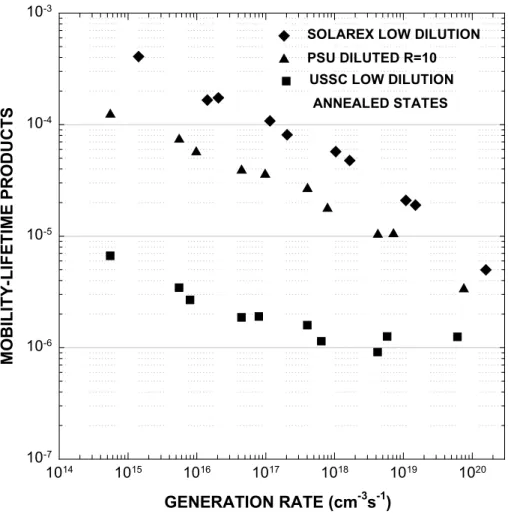
A comparison was made between hydrogen-diluted (R=10) materials from Penn State and “low” dilution materials from BP Solarex and Uni-Solar, where all of these materials have produced high performance solar cells. There are two interesting aspects to the results presented here for the annealed state. The first is the similarity of the three materials deposited under quite different conditions. The other is the difference the three materials exhibit in their relationships between µτ products and α(hν), in spite of the fact that the often misused term “device quality material” is relevant here. Fig. I.2.1 shows the µτ products as a function of generation rate G for the three materials in the annealed state. Compared to PSU diluted material, relatively higher electron µτ products are present in the BP Solarex material and lower electron µτ products in the USSC material. The results of Dual Beam Photoconductivity (DBP) measurements at low generation rate that corresponds to CPM, are shown in Fig. I.2.2. There is a clear discrepancy here with the commonly held view based on the “omnipotence” of the dangling bond, Do, states in that the BP Solarex material has both µτ products as well as subgap absorption at α(1.2eV) higher than those from PSU material, and for Uni-Solar material both the µτ and α(1.2eV) are lower. Such a presence of higher lifetimes with higher subgap absorption directly contradicts the still widely held view that these characteristics are determined solely by the Do states while ignoring the effects of charged defects. The dependence of a-Si:H material properties on charged defects is also found to dominate the characteristics of thin film materials from the Super Lab at ETL. In Fig. I.2.3, the µτ products are shown as function of generation rate G for one of the Super Lab a-Si:H films deposited at Ts =200 oC. Also shown are the results for the PSU diluted
R=10, undiluted, R=0, films prepared at Ts=200 oC. Significant differences in the recombination
kinetics are clearly indicated by the magnitude, and particularly by the shape of µτ(G) curves. It should be remembered that the key claim of the “Do dominated model” is that µτ products are independent of G, i.e. γ is constant and equal to 1 [2]. The presence of charged defects is also evidenced from the more subtle differences in the subgap absorption spectra. Results from The Super Lab for the Ts=200 oC, and from PSU for the R=0 and R=10 films of Fig. I.2.3 are shown
with DBP at a generation rate of 1015cm-3s-1, which is equivalent to that used in CPM, exhibit distinctly different dependences on photon energy. The differences in the fall off of α(hν) at low photon energies are indicative of the relative contribution from defects located above midgap. The contributions from these states are further enhanced at higher generation rates when these states become more occupied by electrons.
The results of subgap absorption and photoconductivity measurements (µτ) have been analyzed using an improved Subgap Absorption Model (SAM) with a five Gaussian distribution of gap states. An iterative procedure for fitting of results such as in Fig. I.2.3 and Fig. I.2.4 is used to obtain a single set of “operational parameters” for the densities, distribution and carrier capture cross-sections of different gap states. An example of such self-consistent analysis is shown for the R=0 and R=10 materials in Fig. I.2.3, where the solid lines are fits to the experimental results for µτ versus G. The corresponding fits for α(hν) with identical parameters are shown in Fig. I.2.4. It should also be pointed out here that the parameters used here are also the same as those used to fit the I~V, QE and FF characteristics of corresponding Schottky barrier cell structures discussed in Section 2.
References
1. L. Jiao, I. Chen, R.W. Collins, and C.R. Wronski, “An Improved Analysis for Band Edge Optical Absorption Spectra in Hydrogenated Amorphous Silicon from Optical and Photoconductivity Measurements”, Applied Physics Letters, 72, 1057-1058, (1998). 2. M. Stutzmann, W.B. Jackson and C.C. Tsai, “Light-induced Metastable Defects in
Hydrogenated Amorphous Silicon: A systematic study”, Physical Review B, 32 23-47 (1985).
Figure I.2.1 Mobility-lifetime products of USSC low dilution, Solarex low dilution and PSU diluted R=10 in annealed state.
GENERATION RATE (cm-3s-1) 1014 1015 1016 1017 1018 1019 1020 MO BI LITY -L IFE T IME P R O D UC T S 10-7 10-6 10-5 10-4 10-3
USSC LOW DILUTION ANNEALED STATES PSU DILUTED R=10 SOLAREX LOW DILUTION
Figure I.2.2 Subgap absorption of USSC low dilution, Solarex low dilution and PSU diluted R=10 in annealed state. ENERGY (eV) 0.9 1.0 1.1 1.2 1.3 1.4 ABSO R PT IO N ( cm -1 ) 10-2 10-1 100 GENERATION RATE=1x1015 cm-3 s-1
USSC LOW DILUTION PSU DILUTED
SOLAREX LOW DILUTION
Figure I.2.3 Mobility-lifetime products of PSU R=10, 0 and ETL materials in annealed state. Symbols are experimental results and the lines are fits.
GENERATION RATE(cm-3s-1) 1014 1015 1016 1017 1018 1019 1020 1021
µτµτµτµτ
(c
m
-3 V -1 ) 10-6 10-5 10-4 PSU R=10 PSU R=0 ETL Ts =200 0C FITSFigure I.2.4 Subgap absorption of PSU R=10, 0 and ETL materials in annealed state. Symbols are experimental results and lines are fits.
ENERGY (eV) 0.9 1.0 1.1 1.2 1.3 1.4 ABS ORP T IO N (cm -1 ) 0.01 0.1 1 PSU R=10 PSU R=0 ETL Ts=200 oC FITS
TASK II: Insights into Improved Stability in Materials and Solar Cells
II.1. Degradation Studies
Results and Discussion
The type, nature and densities of different light induced defects in optimized a-Si:H materials have been investigated and characterized. These studies have been carried out on films and corresponding Schottky barrier cell structures with different thicknesses of the intrinsic bulk layers. Taking into account the inadequacy of the approach based solely on “neutral dangling bonds”, the characterization was expanded in an attempt to include all gap states. We find that light-induced charged defects are as important as the neutral dangling bond defects in determining the properties and stability of a-Si:H materials and solar cells.
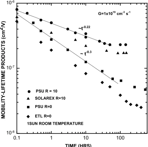
The light induced gap states have been characterized using the methodology described in Task I. This included the self-consistent fitting of all the results on films and corresponding Schottky barrier cell structures with a five Gaussian distribution of gap states. The studies on light-induced changes have been carried out with a-Si:H materials fabricated in different laboratories over a wide range of deposition conditions. Examples of the different light-induced changes in µτ products are shown in Fig. II.1.1 with results on BP Solarex, PSU and ETL materials. Fig. II.1.1 shows the µτ products at a generation rate of G=1x1019 cm-3 s-1 for two diluted and two undiluted materials as function of 1 sun illumination time and the two lines corresponding to t-0.3 and t-0.22 as guides for the eye. Although in the undiluted materials the degradation kinetics can be interpreted in terms of the “famous” t-1/3 dependence, such a dependence is found only in undiluted materials and then at high generation rates such as this 1x1019 cm-3 s-1, which is close to that of 1 sun. The PSU and BP Solarex diluted samples clearly show degradation kinetics which are significantly slower. These studies have also shown that the µτ products obtained at different generation rates exhibit quite different kinetics as seen in Fig. II.1.2, where the µτ products at G=1x10¹⁹ and 1x1016 cm-3 s-1 are plotted as a function of 1 sun illumination time for the PSU undiluted film. A more detailed description of measurements and
results on light-induced changes is presented in Appendix I for diluted a-Si:H films from USSC and PSU. Such a wide range of kinetics, as well as the large, rapid light-induced changes under 1 sun illumination reported previously can not be explained by a Do dominated model, but are entirely consistent with the accompanying creation of charged defects. It can also be noted in Fig. II.1.1 that under 1 sun illumination at room temperature the diluted materials reach a degraded steady state in less than 100 hours, unlike the greater than 1000 hours for undiluted materials.
The importance of taking into account the effects of charged defects is also clearly evident in the detailed evaluation of results in the soaked states. After light-induced degradation and the creation of significant number of dangling bonds, their presence is reflected more strongly in the subgap absorption. Consequently, values such as α(1.2eV) are an indication (not in an absolute terms though) of the densities of Do, but the subgap absorption also depends on the ratio between the densities of the charged defects and the neutral states. This results in subtle but real differences in the shape of the absorption spectra, which can be reconciled with the corresponding difference in µτ products. Results, such as obtained on PSU R=0 and R=10 films after 100 hours of 1 sun illumination, clearly show the similarity of subgap absorption in the two materials with both α(1.2eV) values virtually equal to one. But as seen in Fig. II.1.1, the R=0 materials have µτ products significantly smaller than those of the R=10 material. Detailed self-consistent analysis indicates that the same densities of Do states have been created after the 100 hours 1 sun illumination in both materials, but that more charged defects are present in the R=0 case. It should be pointed out here also that the densities of dangling bonds deduced from the analysis are in very good agreement with those obtained from ESR measurements, which give densities of 8~10x1016 cm-3 for the Do states for both materials. It is also important to note that even with these high densities of Do states, in p-i-n solar cells excellent fill factors are obtained with the R=10 material and not with the R=0 material, further showing the significance of the light-induced charged defects in degrading the performance of a-Si:H solar cells.
Another misconception about the creation of light induced defects is that there is only a limited number of sites available in a given a-Si:H material which can be converted into metastable defects. This is based in part on results which claim that there is no dependence of the degraded steady state densities of defects on either the light intensity or temperatures below 70
oC [Park et al., 1989]. This has in part been responsible for accepting accelerated tests of
light-induced changes with high illumination intensities as being representative of the 1 sun degraded steady states (DSS) and the modeling predictions for end of life efficiencies. Despite the clear indications that this is certainly not true in solar cells [2], because of the very long times needed for undiluted a-Si:H films to reach the 1 sun degraded steady state (DSS), there have not been any independent verifications of such equivalence in films as well as the corresponding solar cells.
As part of the studies here, light-induced degradation with high intensity illuminations were also carried out on diluted films which reach the 1 sun degraded steady state in less than 100 hours at room temperature. Results on a PSU diluted a-Si:H film are shown in Fig. II.1.3 for the µτ products and for α(hν) in Fig. II.1.4 after 1 sun and 10 sun illumination. Degraded steady states for µτ products and α(hν) are reached with both 1 sun and 10sun illuminations, having clearly different values. In addition we find that the 1 sun light-induced changes, even between 25 oC and 75 oC have distinctly different degradation rates as well as values of the µτ products and α(hν) in their respective DSS. Because such dependence of light-induced changes on both temperature and light intensity, the arbitrarily chosen high intensity tests commonly used are irrelevant unless quantified with 1 sun DSS results. In the studies carried out here, the actual 1 sun DSS is evaluated and the defects are characterized with the detailed measurements and modeling of results on both films and Schottky barrier cell structures.
Extensive studies of light induced defects were carried out on diluted (R=10) Schottky barrier solar cell structures and the corresponding films. The measurements on Schottky barrier cell structures, which include forward I-V, light I-V and QE with different i layer thicknesses, are analyzed with results of µτ products and subgap absorption spectra obtained on the
corresponding films. The focus of the work here is mainly on the degraded steady state (DSS) obtained with 1 sun illumination at 25°C in films and Schottky barrier cells. All these results were analyzed using the distribution of gap states shown in Fig. II.1.5, where in addition to the neutral dangling bond D0 states two gaussian distributions of defect states are introduced above and below midgap . Because of the large number of adjustable parameters associated with the energy locations, halfwidths, densities and carrier capture cross-sections of the different gap states, an iterative procedure was adopted for the self-consistent fitting of all the results on the thin films and the Schottky barriers using the same values for the parameters. In the process the relative sensitivity of the different results to specific gap state parameters was established and this is illustrated in Table I.
Table I. Parameters with largest effect on respective characteristics.
µτ Subgap forward I-V light I-V QE
D+*, D0, D+(E)
D0, D+, D- D+(E), D+*(N) D0, D+*, VB(tail)
α, D0, D+*, VB(tail)
E: energy location only N: density only
The characteristics of Schottky barrier solar cell structures with different thickness protocrystalline (R=10) i layers, were fitted using the gap state distribution shown in Fig. II.1.5 and the same parameters were used in fitting the results on the thin film materials. This is discussed in detail in Appendix 2 with the I-V characteristic being discussed here.
As an example, the forward bias dark current characteristics are shown in Fig. II.1.6, where the symbols are the experimental results for cells with 0.2, 0.5 and 0.7µm thick i-layers in the 1 sun degraded steady state (DSS). Also shown are results for the 0.7µm cell in the annealed state (AS). At low forward bias, the currents are controlled by the Schottky barrier height for electron, φBN=0.97eV, and have an exponential region before they become limited by the bulk,
and thus the thicknesses of the i layers. In addition Fig. II.1.6 shows that the light induced defects have a very large effect whereby in the case of the 0.7µm cell that the far forward bias
currents decrease over 5 orders of magnitude. The simulation results of these three cells, using the same “operational” parameters as in Fig. II.1.5, are shown as solid lines in Fig. II.1.6. Very good agreements are obtained for all three cells up to 2V.
Corresponding fits to the mobility-lifetime product (µτ) and the subgap absorption with two generation rates for the corresponding R=10 thin film materials are shown in Fig. II.1.7, where the symbols are the experimental results and the lines are the fits using the same gap state parameters as used in Fig. II.1.6. It may be pointed out that the values of the µτ products at each generation rate correspond to an individual result, just as in the case of the quantum efficiencies for the different wavelengths. The good fits of both the µτ products and the subgap absorption using the same ‘operational’ gap state parameters as in the corresponding Schottky barrier solar cell structures clearly support the importance of including charge defects in any realistic characterization of gap state and their effect on cell performance. However the distribution of states chosen to represent charged defects is not unique but rather a possibility, nevertheless, the “operational” parameters such as derived here offer a more realistic and reliable approach for modeling of p-i-n and n-i-p solar cells characteristics in their degraded steady state.
A better understanding of the contributions that the different gap states make to the degradation will help to further quantify their parameters and to obtain self-consistent fits for all the cell characteristics. To assess the effects of the various gap states on the different film results and Schottky barrier cell characteristics, sensitivity studies were carried out where the values of the densities, energy positions and electron-hole capture cross-sections were individually changed. The results of these were used in obtaining the self-consistent fits to the Schottky barrier characteristics, presented in Appendix II, as well as the analysis of p-i-n solar cell characteristics discussed in Section 3.
References
1. H.R. Park, J.Z. Liu and S. Wagner, “Saturation of the Light-Induced Defect Density in Hydrogenated Amorphous Silicon”, Appl. Phys. Lett. 55, 2658-2660 (1989).
2. L. Yang, L. Chen and A. Catalano, “Intensity and Temperature Dependence of Photodegradation of Amorphous Silicon Solar Cells under Intense Illumination”, Appl.
Figure II.1.1 Kinetics of light-induced changes of PSU R=10, 0, Solarex R=10 and ETL R=0 materials. 0.1 1 10 100 M O BI LI TY-L IF E T IM E PRO DUCTS ( c m 2 /V ) 10-8 10-7 10-6 PSU R = 10 TIME (HRS) ~ t-0.3 ETL R=0 PSU R=0 SOLAREX R=10
1SUN ROOM TEMPERATURE
~t-0.22
Figure II.1.2 Kinetics of light-induced change of PSU R=0 materials at two generation rates. TIME (HRS) 10-1 100 101 102 M O BI LI T Y -L IF E T IM E PRODUCT ( c m 2/V ) 10-8 10-7 10-6 ~ t-0.25 ~ t-0.30 G=1.6x1016cm-3s-1 G=1.0x1019cm-3s-1 PSU R = 0 FILM
Figure II.1.3. Kinetics of light-induced changes of PSU R=10 materials at two light intensities. TIME (HRS) 0.1 1 10 100 M O BI L ITY-L IF ET IM E PRODUCT S (c m 2 /V ) 10-6 PSU DILUTED R=10 1 SUN 50 oC 10 SUN 50 oC G=1x1019 cm-3 s-1
Figure II.1.4. Subgap absorption of PSU R=10 material in degraded steady state at 1 sun and 10 sun illumination. Energy (eV) 0.9 1.0 1.1 1.2 1.3 1.4 Ab s o rp ti on ( cm -1 ) 10-1 100 101
1 SUN 50 OC STEADY STATE α(α(α(α(1.2eV)=0.87
LOW GENERATION RATE
10 SUN 50 OC STEADY STATE αααα(1.2eV)=1.29 PSU DILUTED R=10
Figure II.1.5. Distribution of gap states used in the analysis of the Schotky barrier cell results in the 1 sun degraded steady state. D0 are the neutral dangling bonds, D+, D+* are the positively charged and D-, D-* are the negatively charged states.
ENERGY(eV)
0.0
0.4
0.8
1.2
1.6
D
E
N
S
ITIES OF STA
T
ES(
cm
-3)
10
1410
1610
1810
2010
2210
1410
1610
1810
2010
22D
+*
E
C
E
V
D
+
D-*
D
-
D
o
Figure II.1.6. Forward I-V characteristics of 0.2, 0.5 and 0.7 µm n-i Schottky barrier cells in the degraded steady state (DSS). Symbols are experimental results and solid lines are fits. Also shown are results for the 0.7µm in the annealed state (solid symbols).
Figure II.1.7. Subgap absorption characteristics of PSU R=10 materials in the degraded steady state (DSS). Symbols are experimental results and solid lines are fits. Also shown are fit to mobility-lifetime products results in DSS.
ENERGY (eV) 0.9 1.0 1.1 1.2 1.3 1.4 1.5 1.6 1.7 1.8 1.9 2.0 A B SO RP TION CO EFFIC IENT (cm -1 ) 10-1 100 101 102 103 104 GENERATION RATE (cm-3 s-1) 1014 1015 1016 1017 1018 1019 1020 1021 µτ ( µτ ( µτ ( µτ ( V/ cm 2 ) 10-7 10-6 10-5 100HRS 1SUN T&R G=1015 cm-3 s-1 G=1017 cm-3 s-1 SAM FITS
TASK III: Optimization of Solar Cell Performance with Improved Intrinsic
Layers
III.1. Optimization of p/i Interfaces
Motivation and Overview
Many studies relating the processing procedure to device characteristics have demonstrated the critical role of interfaces in the performance of hydrogenated amorphous silicon (a-Si:H) solar cells. [1] For example, controlled deposition of wider band gap layers at the p/i and i/p interfaces of a-Si:H p-i-n and n-i-p heterojunction solar cells has demonstrated effects on the open-circuit voltage Voc at the monolayer (ML) level of incorporation. [2-4] Non-invasive real time spectroscopic ellipsometry (RTSE) is a powerful technique that can characterize changes in surface coverage on the order of 0.1 ML, and can provide the optical properties for layers as thin as ~5 Å. [5] In addition, the wide dynamic range of RTSE data provides the effective thickness evolution of a-Si:H films ranging from 0.1 Å to 5000 Å. In this Task, we have succeeded in identifying and quantifying three different effects that occur at the surface and sub-surface of the amorphous silicon-carbon (a-Si1-xCx:H) layer before a-Si:H i-layer deposition in the p-i-n solar cell configuration. These effects include (i) contamination of the p-layer surface, (ii) structural equilibration of the p-layer leading to H emission, and (iii) p-layer surface temperature variations. Only by separating the effects can RTSE unambiguously describe interface formation and thereby develop processing procedures for optimized devices.
Experimental Details
For the RTSE studies in which surface contamination dominates, 200 Å a-Si1-xCx:H p-layers were prepared by PECVD using diborane doping gas and flow ratios of [SiH4]:[CH4]:[B2H6]:[H2] =6:4:0.01:0.99 [in stand. cm3/min (sccm)]. Substrates for RTSE consist of 440 Å SnO2:F on c-Si wafers, which provide relatively smooth surfaces
![Figure I.1.1 Surface roughness layer thickness (d s ) versus bulk layer thickness (d b ) from RTSE data collected during the preparation of Si films with R=[H 2 ]/[SiH 4 ]=15, 30, and 80](https://thumb-eu.123doks.com/thumbv2/123doknet/12700678.355621/23.918.191.754.217.672/figure-surface-roughness-thickness-versus-thickness-collected-preparation.webp)

![Figure I.1.6 Broadening parameter plotted versus optical gap at 200°C for a-Si 1-x C x :H (0≤x≤0.23) films prepared at different flow ratios [CH 4 ]/{[SiH 4 ]+[CH 4 ]} from 0 to 0.8 (open circles) and for a-Si:H films prepared at different H 2 -dilution ra](https://thumb-eu.123doks.com/thumbv2/123doknet/12700678.355621/28.918.152.758.144.776/figure-broadening-parameter-prepared-different-prepared-different-dilution.webp)