HAL Id: hal-00648719
https://hal.archives-ouvertes.fr/hal-00648719
Submitted on 17 Apr 2018
HAL is a multi-disciplinary open access
archive for the deposit and dissemination of
sci-entific research documents, whether they are
pub-lished or not. The documents may come from
teaching and research institutions in France or
abroad, or from public or private research centers.
L’archive ouverte pluridisciplinaire HAL, est
destinée au dépôt et à la diffusion de documents
scientifiques de niveau recherche, publiés ou non,
émanant des établissements d’enseignement et de
recherche français ou étrangers, des laboratoires
publics ou privés.
Exploring FPGAs Capability to Host a HPC Design
Clément Foucher, Fabrice Muller, Alain Giulieri
To cite this version:
Clément Foucher, Fabrice Muller, Alain Giulieri. Exploring FPGAs Capability to Host a HPC
De-sign. Norchip 2010, Nov 2010, Tampere, Finland. pp.1-4, �10.1109/NORCHIP.2010.5669494�.
�hal-00648719�
Exploring FPGAs Capability to Host a HPC Design
Cl´ement Foucher, Fabrice Muller and Alain Giulieri
Universit´e de Nice-Sophia Antipolis
Laboratoire d’ ´Electronique, Antennes et T´el´ecommunications (LEAT) CNRS UMR 6071, Bat. 4, 250 rue Albert Einstein
06560 Valbonne, France
{Clement.Foucher, Fabrice.Muller, Alain.Giulieri}@unice.fr
Abstract—Reconfigurable hardware is now used in high performance computers, introducing the high performance reconfigurable computing. Dynamic hardware allows processors to devolve intensive computations to dedicated hardware circuitry optimized for that purpose. Our aim is to make larger use of hardware capabilities by pooling the hardware and software computations resources in a unified design in order to allow replacing the ones by the others depending on the application needs. For that purpose, we needed a test platform to evaluate FPGA capabilities to operate as a high performance computer node. We designed an architecture allowing the separation of a parallel program communication from its kernels computation in order to make easier the future partial dynamic reconfiguration of the processing elements. This architecture implements static softcores as test IPs, keeping in mind that the future platform implementing dynamic reconfiguration will allow changing the processing elements.
In this paper, we present this test architecture and its implementation upon Xilinx Virtex 5 FPGAs. We then present a benchmark of the platform using the NAS parallel benchmark integer sort in order to compare various use cases.
Index Terms—FPGA, Architecture Exploration, High Performance Reconfigurable Computing
I. INTRODUCTION
Field Programmable Gate Arrays (FPGAs) consideration evolved from original glue-logic purpose to a real status of component of a design. Modern FPGAs allow mapping complex component such as digital signal processors, video decoders or any other hardware accelerator. FPGAs are flexible resources, allowing notably hosting devices which nature is unknown at the time of circuit design. For example, a video decoder can allow various compression types and adapt the hardware circuitry according to the current played format. Moreover, the late Partial Dynamic Reconfiguration (PDR) technol-ogy breaks the monolithic status of FPGAs by allowing changing only one part of the device. On a multi-IP design, this allows changing an IP while others are running. FPGA can then be considered as an array of independent IPs. Birk and Fiksman [1] compare reconfiguration capabilities, such as multiple simultaneous IP instantiations, to the software concept of dynamic libraries.
High Performance Computers (HPCs) are large pools of Processing Elements (PEs) allowing massively parallel processing. The main current HPC architectures are discussed by Hager and Wellein [2], while a more abstract study including software is done by Skillicorn [3]. The general topology is a system composed of nodes linked by a network, each node being composed of various PEs. Most common memory systems are globally distributed, locally shared. This means a node’s PEs share the local memory, while the global system consists of many separated memory mappings.
HPCs make use of dynamic hardware for a few years now, intro-ducing the High Performance Reconfigurable Computers (HPRCs). These systems add dynamic hardware resources jointly to the General-Purpose Processors (GPPs). These resources can be used by
the GPPs to map a hardware circuitry specific to the running program in order to increase performance of a specific computation.
El-Ghazawi [4] presents two approaches to reconfigurable archi-tectures: Uniform Node, Nonuniform Systems (UNNSs) and Nonuni-form Node, UniNonuni-form Systems (NNUSs). In UNNSs, the system contains two kinds of nodes; software nodes containing processors, and hardware nodes containing FPGAs. Conversely, in NNUSs, the system consists in a single type of node, each containing both hardware and software PEs. In NNUSs, dynamic resources are generally deeply linked with software PEs located on the same node. This allows high bandwidth between hard and soft resources thanks to dedicated interconnections. Such systems consider the reconfigurable resources as dynamic coprocessors, which are used to replace a specific portion of code.
Our aim is to set up a NNUS-like HPRC architecture which flexibility is increased compared to standard HPRCs. Instead of standard HPC coupled to slave reconfigurable resources, we tend to develop a fully FPGA-based system. In this system, hardware and software resources should be same-level entities, meaning that the type, number and repartition of PEs should be decided depending on the application requirements. This differs from the standard behav-ior of running the program on software processors that instantiate hardware resources when needed. Additionally, the PDR technology should be used to map various independent PEs on the same FPGA, controlling their behavior separately. Doing so requires separating kernels computations from program communication in order to handle PEs reconfiguration independently of the global architecture and interconnect.
To that extent, we needed to build a test platform in order to make sure that such architecture is suitable for standard FPGA resources. Especially, the major point was the communication and memory accesses, which are known bottleneck in current designs. In this paper, we focus on that test architecture. This architecture is not intended to demonstrate the reconfiguration capabilities, and though do not implement PDR of IPs. Instead, we use static software processors to represent generic IPs and use SMP (Symmetric Multi-Processing / Shared-Memory Paradigm) systems as a base.
We present a theoretical view of this architecture, also with a platform implementing this architecture based on the Xilinx Virtex 5 FPGA device. We use the industry standard Message Passing Inter-face (MPI) for the program communication to ensure compatibility with most existing programs. We benchmarked this platform using the NAS Parallel Benchmark Integer Sort (NPB IS) in order to evaluate what improvements will be needed for the future dynamic platform. In section II, we present the model of the architecture we devel-oped, and its implementation on Xilinx Virtex 5 FPGA. In section III, we detail the benchmarking process we run on the platform and its conclusion. Lastly, in section IV, we present related work showing
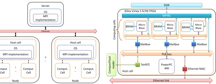
Ethernet Server OS MPI implementation Host cell Comput. Cell Comput. Cell Comput. Cell Comput. Cell OS MPI implementation Host cell OS MPI implementation Node Node n … i … j …
Fig. 1. System Architecture.
the importance of the memory bandwidth, the weak point of our architecture.
II. ARCHITECTURE ANDPLATFORM
The following architecture is intended as a test architecture for the execution of MPI programs. One concern was that it should be easy to run existing programs while making as few changes as possible to the source code. Ideally, these changes could be done automatically by a pre-compiler, so that existing MPI programs could be used directly without any manual changes being required. We present the method we used to adapt the existing bench to our platform.
A. Architecture
The main constraint of our architecture is that communications have to be separated from computations. Communications have to use the MPI protocol, while the kernel computation must be run on separate PEs in order to be easily replaceable by hardware accelerators.
In our model, the system consists in nodes, themselves containing various PEs called cells. On each node, one special cell, called the host cell, is dedicated to communication. The other cells, called the computing cells, are intended to run the kernels. Fig. 1 shows a generic implementation of this system with n nodes, each containing a varying number of computation cells and one host cell.
The host cell should have an external connection such as Ethernet linking the nodes, and must be able to run an implementation of the MPI protocol. The MPI protocol needs a substantial software stack to manage jobs and network communication; thus, we need to use an Operating System (OS) which is able to manage these constraints. By contrast, the computing cells only need to run a single computing thread at any given time, which means that there is no need for a complex OS; a simple standalone application able to run a task and to retrieve the results is sufficient.
Since based on MPI, any computer connected to the same network as the nodes and running the same MPI implementation should be able to start an application on the system. We call such a computer a server on our system.
B. FPGA-based Platform
To implement our nodes, we chose the Xilinx ml507 board, shipped with a Virtex 5 fx70t FPGA, which contains a hardwired PowerPC
PowerPC 440 Ethernet link Ethernet MAC PLB bus DDR MPMC Host cell
Xilinx Virtex 5 fx70t FPGA
Computing cell s Micro Blaze Mailbox Micro Blaze Mailbox Micro Blaze Mailbox SysACE Compac tFlash read er
BRAM BRAM BRAM
Fig. 2. Node Configuration.
440.
The host cell has an Ethernet Media Access Component (MAC) to communicate with other cells. The local memory is a 256 MB DDR2 RAM accessed through a Multi-Port Memory Controller (MPMC) that manages up to 8 accesses to the memory. The mass storage is provided by a CompactFlash card. All these elements are linked to the PowerPC through a PLB bus.
Each computation cell is composed of a MicroBlaze processor plugged into a PLB bus, and of a local memory containing the runtime program. This memory is implemented via Virtex 5’s Block RAMs (BRAMs), and so it has one-cycle access, which is as fast as cache memory. Processor cache is enabled on the DDR memory range. The MicroBlaze has two MPMC connections, for data and instruction cache links. Because MPMC is limited to 8 memory accesses, we also built an uncached version, where all memory accesses are done through the PLB bus, in which case only one link is used for data and instructions alike. Thus, with uncached implementation, we can have up to seven computing cells, whereas the cached version is limited to three cells.
The platform’s buses and processors run at 100 MHz, except for the PowerPC, which runs at 400 MHz. Each computation cell has a link to the host cell using a mailbox component. The mailbox is a simple bidirectional FIFO thanks to which 32-bit messages can be sent between two buses. By plugging one end into the host cell’s bus, and the other end into a computation cell’s bus, we have a very simple message passing mechanism. This mechanism is not optimized, but sufficient for short orders transmission.
Since both the PowerPC and the MicroBlazes are linked to the same DDR through the MPMC, data can be exchanged using the shared memory paradigm, with the mailbox being used for short control messages (e.g. transmitting the pointer to a shared memory section). The whole node configuration is displayed in Fig. 2 (exam-ple of two computing cells uncached, and one cached).
The Virtex 5 fx70t contains 44,800 Look-Up Tables (LUTs), 5,328 KB of BRAM and 128 DSP48Es, which are small DSPs allowing for example a multiplication. After synthesis of the platform, we check the device occupation. Table I presents the used resources along with the FPGA occupation.
We see that the BRAMs are the limiting factor, allowing a maximum of 7 uncached computation cells or 3 cached computation
TABLE I RESOURCES
Resource Uncached Cached Host cell
occupation computing cell computing cell
LUTs 3870 (8.6%) 4441 (9.9%) 2559 (5.7%)
BRAMs 17 (11.5%) 34 (23.0%) 23 (15.5%)
DSP48Es 6 (4.7%) 6 (4.7%) 0 (0.0%)
cells along with 1 host cell, meeting the memory accesses limitation. Nevertheless, current devices like Xilinx Virtex 6 and Virtex 7 are denser in terms of elements, and thus allow bigger IPs. This allows a great flexibility for the future hardware accelerators that will replace the PEs, and could allow for IPs duplication for SIMD implementation.
C. Software Stack
The host cell runs an embedded Linux system. For the MPI implementation, we chose MPICH2 due to its modularity (the sched-uler can be changed, for example). This will be helpful in future developments of the platform in order to take into account the hardware, reconfigurable characteristics of the PEs.
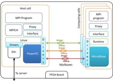
To run an existing MPI program on our platform, it must be split into two parts: first, the computation kernels, and second, the MPI calls for the communication between processes. These two parts are run respectively on the computing cells and the host cell. The stack used for the communication between the host cell and the computing cells is shown in Fig. 3.
The bottom level of the stack consists in a layer known as the interface, which is able to send and receive orders and basic data types through the mailboxes. The interface is independent from the MPI program. The upper level consists in a proxy, which transforms calls to kernels into a succession of calls to the interface in order to transmit the parameters and the run order to the computing cells. Conversely, on the MicroBlazes, the calls to MPI primitives are replaced by calls to the proxy, which transmits the orders to the PowerPC, eventually making the MPI call.
Unlike the interface, the proxy is deeply linked to the running program. Indeed, it takes on the appearance of the existing C functions so as to be invisible to the original program. In this way, the program does not need to be modified, the only change being the separation of the kernels from the MPI calls, and the writing of a simple proxy layer.
III. EXPERIMENTALRESULTS
As the benchmark, we chose a simple integer sort. Integer sort implies exchanging arrays of integers between the PEs, what allows testing the communications performances. It is not intended to check the computation performances, rather the impact of jobs dispatching. A. The NPB IS Bench
NASA Advanced Supercomputing (NAS) proposes a set of bench-marks, the NAS Parallel Benchmarks (NPB) [5], containing eleven tests intended to check HPC performance. Each benchmark tests a particular aspect, such as communication between processes or Fourier transform computation performances. The benchmarks are proposed using different implementations, including MPI for message passing platforms and OpenMP for shared memory machines.
We chose the Integer Sort (IS) benchmark because it can be used to test communication speeds and computation times, and because of its C implementation, whereas most of the benches are written in Fortran (there is no Fortran compiler for MicroBlaze). The NPB
FPGA Board Host cell MicroBlaze Mailboxes Interface Proxy MPI program PowerPC Linux Interface D r i v e r s Proxy MPI Program MPICH Eth. Drivers Runtime D r i v e r s Computing cell s To server
Fig. 3. Software Stack.
benches can be run using various classes, each class representing a different amount of data to match different HPC sizes. The possible classes for the IS bench are, in ascending order, S, W, A, B, C and D.
IS is a simple program that sorts an integer array using the bucket sort algorithm. The number of buckets depends on the number of processes, and can be adjusted to choose the parallelism level. The number of processes should always be a power of two.
Each MPI job owns some buckets, in ascending order (job 0 will get the lower-range buckets). Each MPI job also owns a part of a big randomly-filled array of integers. Each job performs a local ranking to identify the bucket to which each integer belongs. Then, total number of integers in each bucket is summed upon all the jobs. Finally, the content of each bucket on each job is sent to the job owning that bucket.
B. Establishing the Bench
In order to run the NPB IS bench on our platform, we had to modify it to match our architecture, the first step being to separate the MPI communication from the sorting algorithm. The basic test includes an option to separate communication timings from computation timings, what has been enabled to have a detailed view of the repartition impact.
We build the proxy the following way: the function intended to reside on the host cell and on the computing cells are separated. In the host cell code, the kernel function headers are preserved, while their body is replaced by calls to the interface to build the proxy. On the computing cells, we build a proxy layer that calls the kernels when receiving an order from the host cells. The computing cells do not have the notion of MPI. So a dummy MPI interface is written in the proxy, which does the calls to the interface in order to transmit the communication orders to the host cell.
We chose class A for the bench as a tradeoff between a minimum size correctly representing HPC applications and a maximum size that was reasonable given our limited number of boards.
C. Bench Results
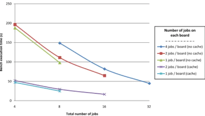
We had thirteen ml507 boards based on Xilinx Virtex 5 that we configured with the cached or uncached platform, and linked using Ethernet. The server, connected to the same network, was a standard x86 64 PC running Linux and MPICH2. Whenever possible we put,
0 50 100 150 200 250 4 8 16 32 B e n ch e xec u tion tim e ( s)
Total number of jobs
4 jobs / board (no cache) 2 jobs / board (no cache) 1 job / board (no cache) 2 jobs / board (cache) 1 job / board (cache) Number of jobs on each board
Fig. 4. NPB IS Bench Execution Times versus Jobs Number and Repartition.
on each board, a number of processes equal to a power of two. Since the number of boards was however limited, not all configurations were available: for example, having 32 cached processes would require at least 16 boards; or attempting to run the entire bench on a single board would have exceeded the memory available.
For the cached version, we activated only the instruction cache, and disabled the data cache. This was necessary since, while the instruction part consists of a relatively small loop applied to the data (clearly in line with the cache principle), the data itself is composed of very large arrays which are processed once before being modified by a send and receive MPI call. Thus, caching the data means that more time is spent flushing and updating cache lines than is saved thanks to the cache. Activating cache upon data not only takes more time than the instruction-only cached version, but also than the uncached version, the additional time being about 10% of the uncached version time. Note that this is entirely application-dependant, and enabling data cache could be of potential interest on an application that does more iterations on smaller arrays.
Fig. 4 shows the total execution times, including computation and communication, versus the number of processes composing the bench. The different curves represent the dispatching of the processes. The horizontal axis tells us that the higher the number of processes, the shorter the execution time, as one would expect from a parallel application. By contrast, the vertical axis tells us that more processes on the same board means a longer execution time. This is because access to the memory is shared: when cells are working, there are concurrent accesses, since the bench is being run in Single Program Multiple Data (SPMD) mode. Since however the memory can be accessed only by one cell at a time, there is often a cell waiting to access memory, and no computation can take place during this waiting time. This issue of waiting time is even more of a concern for uncached platforms, due to the need to constantly fetch the instruction from the memory. The more computation cells are active on the same node, the more concurrent access there are, and the more time is lost waiting.
Much of the time spent waiting could be avoided by using local memory containing computing cells’ data, and using a dedicated Network On Chip (NOC) to exchange data between cells on the same node.
IV. RELATEDWORK
Gothandaraman [6] implements a Quantum Monte Carlo chemistry application on FPGA-based machines. They implement the kernels the hardware way, drawing on the hardware’s pipelining capabilities.
The tests are run on two platforms: an Amirix Systems AP130 FPGA connected to a dual-processor 2.4 GHz Intel Xeon, and a Cray-XD1 HPC. The main difference between the systems is that the first one has a standard PCI connection between the processor and the FPGAs, while the other implements a high bandwidth Cray’s proprietary RapidArray fabric. Their tests also highlight the memory bandwidth issue, with the acceleration ratio compared to software varying from 3x in the first architecture to 25x in the second one.
The work done by Kuusilinna [7] attempt to reduce memories parallel access issues by using parallel memories. These memories allow non-sequential accesses by following pre-defined patterns. This technique relies on the bank-based memory repartition to store data.
V. CONCLUSION
The FPGA-based nodes architecture we depicted in this article differs from general HPC nodes by introducing a physical separation of the PEs intended for communication and computation, whereas classic configurations use GPPs to do both. With classic configurations, an OS manages the whole node, including communication and task scheduling, even if in HPRC, some tasks are delocalized on the hardware accelerators. In our design, the OS is only intended for MPI management, and ideally could be avoided and replaced by a hardware-based communicating stack.
Our work highlights the memory issues inherent to shared memory architectures. We conclude that a SMP platform is not adapted to the FPGA implementation we target. Concurrent data treatment requires not only sufficient bandwidth, but also the ability to supply data to processes in a parallel manner.
This means a distributed memory architecture should be more suited for this use, meeting the manycore architectures. Like manycore architecture, a NOC should be more adapted. This implies adding local memory to the cells, but we saw that the BRAM capacity is limited. Fortunately, current and future FPGA releases will include growing memory sizes. As an example, a Virtex 7 v2000t does contain 55,440Kb of BRAM, where our Virtex 5 fx70t contains only 2,160Kb.
Because of ARM predominance in low power IP cores, which are adapted to FPGAs, one course of future exploration will be to center our platform on ARM processors. In particular, we will study the ARM AMBA AXI bus to check if its characteristics make it suitable for use as a NOC.
REFERENCES
[1] Y. Birk and E. Fiksman, “Dynamic reconfiguration architectures for multi-context fpgas,” Comput. Electr. eng., vol. 35, no. 6, pp. 878 – 903, 2009. [Online]. Available: http://www.sciencedirect.com/science/article/ B6V25-4VH32Y8-1/2/303db6d9659170441ea21e32c5e9a9d2
[2] G. Hager and G. Wellein, Architecture and Performance Characteristics of Modern High Performance Computers, S. B. . Heidelberg, Ed., 2008, vol. 739/2008.
[3] D. B. Skillicorn and D. Talia, “Models and languages for parallel computation,” ACM Comput. Surv., vol. 30, no. 2, pp. 123–169, 1998. [4] T. El-Ghazawi, E. El-Araby, M. Huang, K. Gaj, V. Kindratenko, and
D. Buell, “The promise of high-performance reconfigurable computing,” Computer, vol. 41, pp. 69–76, 2008.
[5] W. Saphir, R. V. D. Wijngaart, A. Woo, and M. Yarrow, “New imple-mentations and results for the nas parallel benchmarks 2,” in In 8th SIAM Conference on Parallel Processing for Scientific Computing, 1997. [6] A. Gothandaraman, G. D. Peterson, G. L. Warren, R. J. Hinde, and
R. J. Harrison, “Fpga acceleration of a quantum monte carlo application,” Parallel Comput., vol. 34, no. 4-5, pp. 278–291, 2008.
[7] K. Kuusilinna, J. Tanskanen, T. H¨am¨al¨ainen, and J. Niittylahti, “Config-urable parallel memory architecture for multimedia computers,” J. Syst. Archit., vol. 47, pp. 1089–1115, August 2002.