• Aucun résultat trouvé

Unusually long carrier lifetime in a Mott insulator revealed by time-resolved Photoemission Electron Microscopy

N/A
N/A
Protected

Academic year: 2021

Partager "Unusually long carrier lifetime in a Mott insulator revealed by time-resolved Photoemission Electron Microscopy"

Copied!
3
0
0

Texte intégral

(1)

HAL Id: hal-03092636

https://hal.archives-ouvertes.fr/hal-03092636

Submitted on 2 Jan 2021

HAL is a multi-disciplinary open access

archive for the deposit and dissemination of

sci-entific research documents, whether they are

pub-lished or not. The documents may come from

teaching and research institutions in France or

abroad, or from public or private research centers.

L’archive ouverte pluridisciplinaire HAL, est

destinée au dépôt et à la diffusion de documents

scientifiques de niveau recherche, publiés ou non,

émanant des établissements d’enseignement et de

recherche français ou étrangers, des laboratoires

publics ou privés.

Unusually long carrier lifetime in a Mott insulator

revealed by time-resolved Photoemission Electron

Microscopy

Danylo Babich, Keiki Fukumoto, Benoit Corraze, Julien Tranchant, Maciej

Lorenc, Hervé Cailleau, S-Y Koshihara, Laurent Cario, Etienne Janod

To cite this version:

Danylo Babich, Keiki Fukumoto, Benoit Corraze, Julien Tranchant, Maciej Lorenc, et al.. Unusually

long carrier lifetime in a Mott insulator revealed by time-resolved Photoemission Electron Microscopy.

Frontiers in Optics / Laser Science (2020), paper LTu8F.3, Sep 2020, Washington, United States.

�hal-03092636�

(2)

LTu8F.3.pdf Frontiers in Optics / Laser Science © OSA 2020

Unusually long carrier lifetime in a Mott insulator revealed

by

time-resolved Photoemission Electron Microscopy

Danylo Babich1, Keiki Fukumoto2, Benoit Corraze1, Julien Tranchant1, Maciej Lorenc3, Hervé Cailleau3, S-Y Koshihara4, Laurent Cario1, Etienne Janod1

1 Institut des Matériaux Jean Rouxel (IMN), Université de Nantes, CNRS, 2 rue de la Houssinière, F-44322 Nantes, France 2 High Energy Accelerator Research Organization (KEK), 1-1 Oho, Tsukuba, Ibaraki 305-0801 Japan

3 Univ Rennes, CNRS, IPR (Institut de Physique de Rennes) - UMR 6251, F-35000 Rennes, France 4 Department of Chemistry, Tokyo Institute of Technology, Meguro, Tokyo 152-8551, Japan

etienne.janod@cnrs-imn.fr

Abstract: Mott insulators display puzzling insulator to metal transitions under electric field. We

study here the Mott insulator GaV4S8 using time-resolved Photoemission Electron Microcopy and

reveal unusually long carrier lifetimes, supporting the mechanism of electronic avalanche. OCIS codes: 320.7130; 240.6675

The study in non-equilibrium conditions of an emblematic class of quantum materials, the Mott insulators, is currently developing into an active and fruitful branch of solid state physics. This research field opens up many perspectives by revealing unexpected physical properties based on new control parameters. Mott insulators excited either by ultrafast infrared or THz laser pulses [1,2], or by electric fields [3]display indeed non-trivial insulator to metal transitions (IMT’s) which origin goes beyond the well-established bandwidth- and filling-controlled mechanisms [4]. Interestingly such transitions could be used to build up a new electronics based on Mott insulators, the so-called Mottronics, including breakthrough devices such as Mott memories [3] and artificial neurons for artificial intelligence [5]. A common feature of out-of-equilibrium IMT’s in Mott insulators is that they are based on the massive excitation of electrons from the Lower (valence) to the Upper (conduction) Hubbard Band. For example, recent studies proposed that the multiplication of carrier in a Mott insulator placed under electric field occurs thanks to impact ionization and electronic avalanche [6,7]. However the efficiency of such mechanisms might vanish if carrier lifetime is too small, i.e. if electron-hole recombination due for example to defects is too fast. In classical semiconductors, the carrier lifetime varies from the millisecond in ultrapure silicon to the nanosecond in heavily doped silicon [8,9]. As usual purity levels of Mott insulators are far from the one of ultrapure classical semiconductors, one might naively expect very small carrier lifetime in the nanosecond range. Experimentally, the carrier lifetime in Mott insulators has been scarcely explored, partly due to the lack of appropriate technique to measure it. This situation has recently evolved, with the advent of time-resolved photoemission electron microscopy (tr-PEEM), a technique well-suited to determine carrier lifetime [10]. We report here a tr-PEEM study of the canonical Mott insulator GaV4S8.

GaV4S8 is a Mott insulator exhibiting a lacunar spinel structure (see Figure 1a) built from a NaCl-like arrangement of

GaS4 tetrahedra and V4S4 cubane-like units. In each V4S4 cluster, one out of the seven V 3d electrons is unpaired and

lies on the threefold degenerate molecular t2 level. In the solid, the three narrow bands deriving from these t2 molecular

levels are split by the on-site electron-electron repulsion, leading to an insulating state with a Mott-Hubbard gap of 0.3  0.1 eV [6]. The application of electric field pulses in GaV4S8 leads to an IMT, opening the possibility to use this

compound in memory applications [3]. We performed tr-PEEM experiments at room temperature on the KEK experimental setup [10] on a freshly cleaved GaV4S8 single crystal synthesized as described in Ref. [11]. Figure 1b

provides a schematic description of the electron pathway in a pump-probe tr-PEEM experiment. A first pump laser, either 1.2 eV / 180 fs / repetition rate 500 Hz or 1.1 eV / 10 ns / 200 Hz, promotes electrons in the conduction band. A second laser, the probe, with a tunable delay with respect to the pump expels the excited electrons from the conduction band toward the vacuum level, where electrons are accelerated and detected. A typical tr-PEEM experiment presents the ratio of photoelectrons number detected with and without pump laser versus the time delay between the pump and the probe. Figure 1c shows the results of a first experiment carried out without any pump aiming at establishing the work function  of GaV4S8 and performed by varying the probe energy between 4 and 4.8

eV. This curve displays a clear threshold effect consistent with a work function close to  = 4.6  0.1 eV. For the tr-PEEM experiments, we chose a probe energy of 4.47 eV slightly below the  value, in order to detect only the excited electrons in the Upper Hubbard Band without any pollution by those in Lower Hubbard Band. A first tr-PEEM experiment performed with the 1.2 eV / 180 fs pump laser reveals a striking feature: there is no detectable relaxation of the signal shown in Figure 1d in the 0-100 ps time windows after the pump laser. To confirm this result, a second series of experiment was carried out using the 1.1 eV / 10 ns pump laser. Figure 1e-f shows that the relaxation indeed occurs over a much longer timescale, with a fair description of the relaxation as the sum of three exponential decay terms with1 = 43 ns, 2 = 270 ns and 3 = 4 µs. By comparison with classical semiconductors [8,9], the long carrier

(3)

LTu8F.3.pdf Frontiers in Optics / Laser Science © OSA 2020

Figure 1 : (a) crystallographic structure of GaV4S8 and molecular orbital diagram associated to the V4 tetrahedral cluster. (b) schematic

description of the electron pathway in a tr-PEEM experiment. (c) PEEM energy scan of the probe laser without any pump on a GaV4S8

single crystal. (d-f) tr-PEEM signal vs various ranges of time delay between the pump and the probe in GaV4S8 at room temperature.

lifetime found here might look surprising in a Mott insulator possessing likely a high level of native defects. However, a comparison with other strongly correlated insulators might be more instructive to clarify its origin. Among the scarce studies of carrier lifetime in such compounds, extremely different values are observed, going from the sub-picosecond range in the Mott insulator 1T-TaS2 [12] to 1-20 µs in the strongly correlated insulator VO2 [13]. As proposed in Ref.

[13], a possible clue is the difference of nature and symmetry of the valence and conduction bands states. In a “one-band” Mott insulator like 1T-TaS2, the Lower and Upper Hubbard Bands derive from the same band and therefore

display the same symmetries. In this case, the electron-hole recombination is permitted and hence very fast. Conversely, in a “three-band” Mott insulator like GaV4S8, the top of the LHB and the bottom of the UHB are most

probably made of different and orthogonal V3d bands (see Suppl. Mater. of Ref. [14] and Figure 1a). This would result in a mostly forbidden interband transition and hence in a slow electron-hole recombination. Even if further theoretical and experimental work is required to confirm this conjecture, the possibility to tune the carrier lifetime in Mott insulators by more than six orders of magnitude is of prime interest for artificial intelligence applications. The carrier lifetime is indeed controlling the operating frequency of artificial neurons based on Mott insulators [5]. In summary, we have detected unusually long carrier lifetime in the multiband Mott insulator GaV4S8 usingthe

tr-PEEM technique. This result is important since it supports the proposed mechanism of electronic avalanche [6,7] and will guide the future development of new hardware components in artificial intelligence.

This work was carried out within the French-Japanese International Associated Laboratory IM-LED (CNRS).

References

[1] H. Yamakawa et al., “Mott transition by an impulsive dielectric breakdown”, Nature Materials 16, 1100 (2017).

[2] F. Giorgianni, J. Sakai and S. Lupi, “Overcoming the thermal regime for the electric-field driven Mott transition in vanadium sesquioxide”

Nature Commun. 10, 1 (2019).

[3] L. Cario, C. Vaju, B. Corraze, V. Guiot, E. Janod, “Electric-Field-Induced Resistive Switching in a Family of Mott Insulators: Towards a New Class of RRAM Memories”, Advanced Materials 22, 5193 (2010).

[4] M. Imada, A. Fujimori and Y. Tokura, “Metal-insulator transitions” Rev. Mod. Phys. 70, 1039 (1998).

[5] C. Adda et al., “Mott insulators: A large class of materials for Leaky Integrate and Fire (LIF) artificial neuron », JAP 124, 152124 (2018). [6] V. Guiot et al., “Avalanche breakdown in GaTa4Se8−xTex narrow-gap Mott insulators”, Nature Communications 4, 1722, (2013). [7] P. Diener et al., “How a dc Electric Field Drives Mott Insulators Out of Equilibrium”, Phys. Rev. Lett. 121, 016601, (2018).

[8] M. S. Tyagi and R. Van Overstraeten, « Minority carrier recombination in heavily-doped silicon », Solid-State Electronics 26, 577 (1983) [9] J. A. del Alamo et al., “Modelling of minority-carrier transport in heavily doped silicon emitters”, Solid-State Electronics 30, 1127 (1987). [10] K. Fukumoto et al., “Femtosecond time-resolved photoemission electron microscopy for spatiotemporal imaging of photogenerated carrier dynamics in semiconductors”, Review of Scientific Instruments 85, 083705 (2014).

[11] E. Janod et al., “Negative Colossal Magnetoresistance Driven by Carrier Type in the Ferromagnetic Mott Insulator GaV4S8”, Chem. Mater.,

27, 4398 (2015).

[12] L. Perfetti et al., “Time Evolution of the Electronic Structure of 1T-TaS2 through the Insulator-Metal Transition”, PRL 97, 067402 (2006).

[13] C. Miller et al., “Unusually long free carrier lifetime and metal-insulator band offset in vanadium dioxide”, Phys. Rev. B 85, 085111 (2012). [14] A. Camjayi et al., “First-Order Insulator-to-Metal Mott Transition in the Paramagnetic 3D System GaTa4Se8”, PRL 113, 086404 (2014).

Figure

Figure 1 : (a) crystallographic structure of GaV 4 S 8  and molecular orbital diagram associated to the V 4  tetrahedral cluster

Références

Documents relatifs

ner Vielzahl von Fällen mit der Vereinbarkeit von nationalem Glücksspielrecht mit dem Gemeinschaftsrecht. Es wurde erwartet, dass die aktuelle Placanica-Entschei- dung und zwei

For a given phonon dispersion we thus expect the present data to reduce the slope of the calculated DRR bands since the v F from our experiment are blueshifted with respect to the

experimentally, indicating that the net amount of hydrogens donated by cyclohexene is under-predicted by the model. The ratio of isobutane to isobutene is most sensitive to the

The questions concerned risk factors and consequences of female urinary incontinence, its diagnosis and clinical assessment, urodynamic investigations, conservative

Rubidium superoxide, RbO 2 , is a rare example of a solid with partially filled electronic p states, which allows us to study the interplay of spin and orbital order and other effects

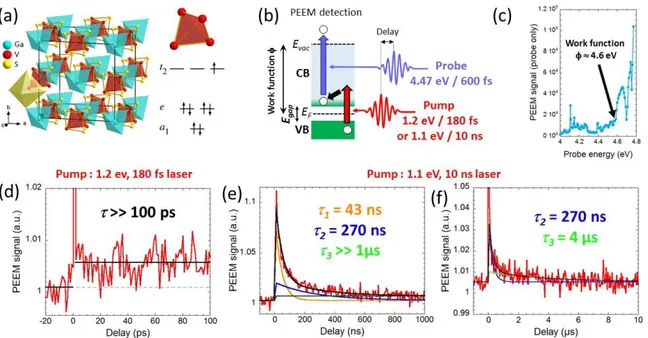
The temperature and field dependence of the signal enable us to discuss the origin of the carrier generation process that leads to population of the Fermi level in this

2-Christophe golay, le droit de peuples à l’autodétermination, publication Europe tiers Monde,Genève,2009.. 3-David harris, The Européen Social charter, press publication

The decomposition of the oxide exposes a 2 × 1 reconstructed surface, characteristic of clean Si(100), ideal for studying the mechanisms of the SOI dewetting process.. The