HAL Id: emse-01099010
https://hal-emse.ccsd.cnrs.fr/emse-01099010
Submitted on 30 Dec 2014
HAL is a multi-disciplinary open access
archive for the deposit and dissemination of
sci-entific research documents, whether they are
pub-lished or not. The documents may come from
teaching and research institutions in France or
abroad, or from public or private research centers.
L’archive ouverte pluridisciplinaire HAL, est
destinée au dépôt et à la diffusion de documents
scientifiques de niveau recherche, publiés ou non,
émanant des établissements d’enseignement et de
recherche français ou étrangers, des laboratoires
publics ou privés.
Analysis of the fault injection mechanism related to
negative and positive power supply glitches using an
on-chip voltmeter
Loic Zussa, Jean-Max Dutertre, Jessy Clediere, Bruno Robisson
To cite this version:
Loic Zussa, Jean-Max Dutertre, Jessy Clediere, Bruno Robisson. Analysis of the fault injection
mechanism related to negative and positive power supply glitches using an on-chip voltmeter. IEEE
Int. Symposium on Hardware-Oriented Security and Trust (HOST), May 2014, Arlington, France.
�10.1109/HST.2014.6855583�. �emse-01099010�
Analysis of the fault injection mechanism related to
negative and positive power supply glitches using
an on-chip voltmeter
Loic Zussa
∗, Jean-Max Dutertre
∗, Jessy Clediere
†, Bruno Robisson
†∗Ecole Nationale Superieure des Mines de Saint-Etienne (ENSM.SE)
Gardanne, France
Email:{loic.zussa,jean-max.dutertre}@mines-stetienne.fr
†Commissariat a l’Energie Atomique et aux Energies Alternatives (CEA)
Gardanne/Grenoble, France
Email:{bruno.robisson,jessy.clediere}@cea.fr
Abstract—Power supply underpowering and negative power supply glitches are commonly used for the purpose of injecting faults into secure circuits. The related fault injection mechanism has been extensively studied: it is based on setup time violations. Positive power supply glitches are also used to inject faults. However, an increase of the supply voltage is not consistent with a mechanism based on setup time violation. Besides, no research work has yet identified the corresponding mechanism. In this work, we report the use of an embedded delay-meter to monitor the core voltage of a programmable device exposed to power supply glitches. It permitted us to gain a further insight into the mechanism associated with power glitches and also to identify the injection mechanism of positive power supply glitches.
I. INTRODUCTION
Secure circuits are targeted by a wide range of physical
attacks. Among these are fault attacks (FA) based on modifying
the circuit environment in order to change its behaviour or to
induce faults into its computations. Fault injection (FI) may be
performed thanks to several means: laser shots, overclocking, underpowering, temperature increase, power supply glitches or electromagnetic pulses. A fine understanding of the properties
and the mechanisms involved with these FI techniques is of
high interest to evaluate the related threats and also to facilitate the design of counter-measures.
Laser FI has a specific mechanism that is well known.
Whereas FI based on setup time violations [1], [2] may be
obtained by various techniques: overclocking , underpowering [1], temperature increase, clock and negative power supply
glitches, and to a certain extent EM pulses. The latter FI
techniques are linked to an increase of the target’s propagation delays over its clock period (see section II).
Positive power supply glitches, despite being a practical fault injection means [3], have been less studied. It can not be explained by a setup time violation because a voltage increase will lead to a decrease of the target’s propagation times, which
is inconsistent with this hypothesis. Its FImechanism has not
yet been ascertained.
In this paper, we report the use of a digital delay-meter
embedded in a programmable device (FPGA) as presented in
[4] and [5] for the purpose of identifying the fault injection mechanism related to positive power supply glitches. It al-lowed us to monitor the core voltage of the device when exposed to positive and negative power supply glitches. It also made it possible to correlate the perturbations induced on the target’s core voltage with the faults injected into an
implementation of the advanced encryption standard (AES[6]).
Our contributions to that research field are:
• An illustration of the use of a delay-meter to monitor the
core voltage of a circuit exposed to power supply glitches,
• An identification of the fault injection mechanism related
to positive power supply glitches,
• An in-depth experimental study of the practice ofFIwith
power supply glitches.
This article is organized as follows. In section II, a reminder of timing constraints and an explanation of how faults may be injected by their violation is provided. In section III, the architecture and principles of the delay-meter used as an
on-chip voltmeter are described. The experimental setup is described in section IV. The obtained experimental results are presented and analyzed in section V. Finally, our findings are summarized in section VI with some perspectives.
II. PRELIMINARIES
In this section the basics of timing constraints are summa-rized. Then the mechanism of fault injection through timing constraint violations is reviewed.
A. Timing constraints
Almost all digital ICs use a common clock signal to
syn-chronize their internal operations. Fig. 1 illustrates the cor-responding architecture. Data are computed by combinatorial
logic (marked P) surrounded upstream and downstream by
register banks made of D flip-flops (DFF) sharing the same
clock signal (clk). n n DpMax n Tclk+Tskew−Tsetup data n clk D Q DFF D D Q DFF clk2q
Fig. 1. Internal architecture of digitalICs.
On a clock rising edge, data are released from the upstream
DFF after a delay Dclk2q which represents the delay between
the clock rising edge and the actual update of a register’s output. Then, these data are processed through the logic before being latched into the next register on the next clock rising
edge. The data propagation time, Dp(data), through the logic
is not constant. It depends on the handled data (those of the current and previous clock periods) and also on the power
supply voltage. DpM ax is the longest propagation time (i.e.
the logic critical time).
A proper functioning of aDFFrequires its input to be stable
all along a time window that extends before and after the clock
rising edge from the setup (Tsetup) and hold (Thold) times
respectively. The data shall not arrive too late nor too early. This arrival constraints can be described mathematically with two timing constraint equations: the setup time timing con-straint expressed in eq. 1 and the hold time timing concon-straint expressed in eq. 2 [7].
Tclk> Dclk2q+ DpM ax+ Tsetup− Tskew (1)
Thold< Dclk2q+ DpM in+ Tskew (2)
where Tskew is the slight phase difference that may exist
between the clock signals at the clock inputs of two different registers due to the clock propagation times through the clock
network, and DpM inis the minimal propagation time through
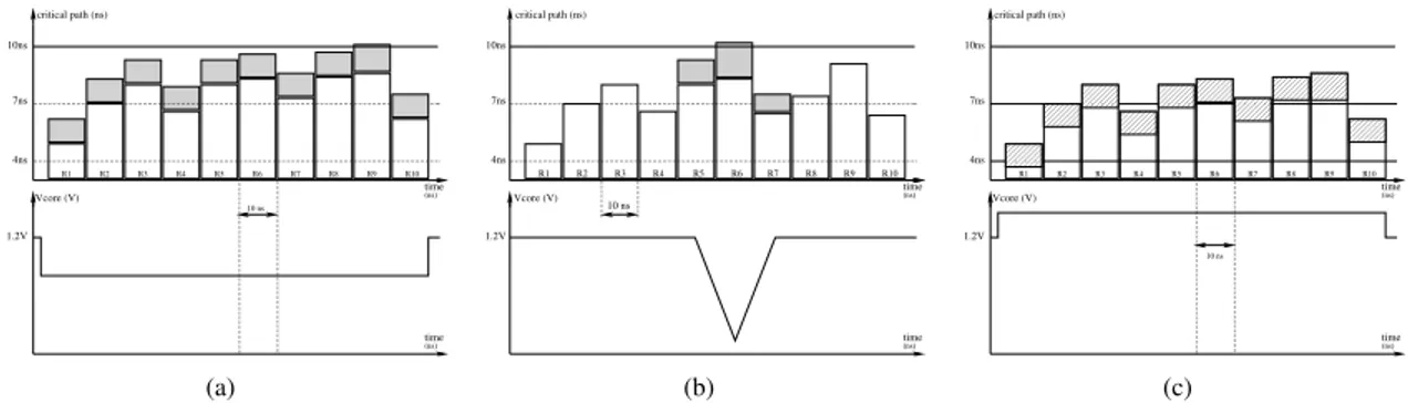
critical path (ns) Vcore (V) 10ns 7ns 4ns 1.2V time (ns) time (ns) R10 R9 R8 R7 R6 R5 R4 R3 R2 R1 10 ns (a) critical path (ns) Vcore (V) 10 ns R10 R9 R8 R7 R4 R3 R2 R1 R5 R6 10ns 7ns 4ns 1.2V time (ns) time (ns) (b) 0000000000000000000000000000000000000000 1111111111111111111111111111111111111111 0000 0000 0000 0000 1111 1111 1111 111100000 00000 00000 11111 11111 111110000000000 00000 00000 11111 11111 11111 11111 00000 00000 00000 11111 11111 1111100000 00000 00000 00000 11111 11111 11111 11111 00000 00000 00000 00000 11111 11111 11111 11111 00000 00000 00000 11111 11111 111110000000000 00000 11111 11111 11111 00000 00000 00000 11111 11111 11111 00000 00000 00000 11111 11111 11111 critical path (ns) Vcore (V) 10ns 7ns 4ns 1.2V time (ns) time (ns) R10 R9 R8 R7 R6 R5 R4 R3 R2 R1 10 ns (c)
Fig. 2. Critical paths of theAES’ rounds when subject to: (a) underpowering, (b) a negative power supply glitch, (c) overpowering.
B. Fault injection due to timing constraints violations The violation of these timing constraints is a means to inject
faults into synchronous integrated circuits (IC).
Previous studies have shown how underpowering a syn-chronous circuit leads to setup time violations [1], [2], [8]. As the target’s supply voltage is decreased, the propagation times through its logic are increased. Consequently, a violation of the setup time constraint may happen when the propagation time increase is large enough: thus a fault is induced. Fig.
2(a) illustrates the effect of underpowering anICimplementing
the AES algorithm (its nominal voltage and clock period are
1.2V and 10ns respectively). The critical times of the AES’
rounds at nominal voltage are depicted in white on the upper curve (they are obviously shorter than the clock period in order to comply with the setup time constraint). The bottom curve represents the decrease of the target’s core voltage (i.e. the underpowering). As a result, the critical times of the
whole AES’ rounds are increased (depicted in grey). In this
illustration a setup time violation occurs during the9th
round. Fig. 2(b) illustrates the effect of a negative power supply glitch: the critical time of the round centered on the glitch (and also those of its neighbors rounds) is increased. As a result, the
setup time violation occurs during the6thround. This allows
an attacker to target a given round, which is mandatory to perform a successful differential fault attack [9].
Fig. 2(c) illustrates the effect of an increase of the tar-get’s core voltage (i.e. overpowering): its critical times are decreased (depicted with grey stripes). No faults were ob-tained because there were neither setup time nor hold time violations (for the latter, the rounds’ propagation times are too large). Note that the illustrations of Fig. 2 are based on actual experiments. We were not able to inject faults into the
AES’ computations by overpowering. However, faults may be
injected in the parts an IC which has very small propagation
times: e.g. a shift register.
Nevertheless, we have successfully injected faults into the
AES’ computations using positive power supply glitches.
Ac-cording to the previous examples, the related FI mechanism
seemed unlikely to be due to setup or hold time violations. It was the main motivation of our work: sensing the core voltage
of an ICwhen exposed to voltage glitches in order to find out
the relevant FImechanism.
III. VOLTMETERDESIGN
Previous experiments [2] on the IC used to carry out the
experimental part of this paper showed that the propagation
times of the IC logic vary linearly with its power supply
voltage. Consequently, measuring the delay of a logic block reveals its supply voltage value. Thus, for the purpose of
monitoring the core voltage of anICexposed to power glitches,
we designed a delay-meter (the so-called voltmeter). Note that this technique has already been introduced and validated by K. Zick et al. [4].
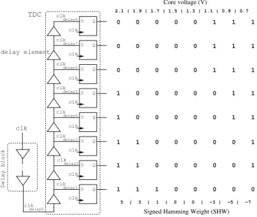
Fig. 3 shows the simplified architecture of the delay-meter. It is made out of two blocks:
• a delay block for which the delay depends on the IC’s
core voltage,
• a time-to-digital converter (TDC [10]) used to obtain a
binary code correlated with the delay.
The input of the delay-meter is the clock signal of the device (clk). It is fed into the delay block to produce a delayed clock, clkdelay(0). The corresponding delay, delay(V dd), depends on
its supply voltage V dd. Then, theTDC is used to convert the
phase difference between clk and clkdelay(0) into a binary
code. TheTDCconsists of a series of 8 delay elements (their
el-ementary delay is δd). Its input is the delayed clock clkdelay(0).
Thus, it provides 8 delayed clocks with an additional delay: n∗δd, where n is the index of the corresponding delay element.
Then, 8DFFs are used to compare the phases of the delayed
clocks with the main clock clk. The output of the nthDFF is
low, resp. high, when clkdelay(n)is in phase advance, resp. in
phase delay, with respect to clk. As a result, the outputs of the
DFFs form an 8-bit vector, which depends on delay(V dd) ([4],
[10]). The right-hand side of Fig. 3 illustrates the obtained output vectors for different settings of the core voltage. As V dd varies, the phase shift between the clock signals also
varies leading to a change in the TDC’s output vector. The
obtained binary code is a thermometer code: it consists in 2 blocks of consecutive ”0” and ”1”. The information it contains is twofold:
• its Hamming Weight (HW),
• the order of these blocks to differentiate e.g. ”000111”
and ”111000”.
Thus, to take into account both these pieces of information,
TDC delay0 delay2 D Q delay8 delay7D Q 0 0 0 0 0 1 1 1 0 0 0 0 0 1 1 1 0 0 0 0 0 1 1 1 1 0 0 0 0 0 1 1 1 0 0 0 0 0 1 1 1 1 0 0 0 0 0 1 1 1 0 0 0 0 0 1 1 1 1 0 0 0 0 0 D Q D Q D Q D Q D Q D Q 2.1 | 1.9 | 1.7 | 1.5 | 1.3 | 1.1 | 0.9 | 0.7 5 | 3 | 1 | 0 | 0 | −3 | −5 | −7 Core voltage (V)
Signed Hamming Weight (SHW)
Delay block clk clk clk delay6 clk delay5 clk delay4 clk delay3 clk clk clk delay1 clk clk clk clk clk clk clk clk delay element clk
Fig. 3. Simplified architecture of the delay-meter (i.e. voltmeter).
”00000111” and ”11100000” were respectively denoted ”+3” and ”-3” (see also Fig. 3).
We used 4 instances of the previous delay-meter (with different delay blocks) to build a voltmeter with a proper voltage measurement range and resolution: 0.7V to 2.4V and around 20mV respectively. Note that the voltage resolution was not constant over the whole measurement range. Fig. 4
displays itsSHWoutput as a function of the core voltage. The
device embedding the voltmeter was exposed to static voltage underpowering to gather the measures used to build this curve. The bijective function corresponding to this curve was used
1 1.5 2 2.5 −5 0 5 Core Voltage (V) Signed Hamming W eight TDC1
Fig. 4. TDCoutputs vs. core voltage.
hereafter to convert the output vectors of the voltmeter into a voltage; despite the fact that the corresponding experiments were carried out with dynamic perturbations (i.e. glitches).
IV. EXPERIMENTALSETUP
In this study we used two different setups, a voltmeter
and an AES, embedded alternately in the same test vehicle:
a programmable circuit (FPGA- Xilinx Spartan3 700A).
A. Pulse generator
We used an Agilent 8114A pulse generator to inject power supply glitches into our test vehicle. This pulse generator is able to produce positive or negative voltage pulses in the 1V to 50V range, with constant fall and rise times equal to 10ns and a tunable pulse width between 10ns and 100ms. The voltage
pulse is centered on a tunableDCvoltage. We used this feature
to provide the voltage supply of the test chip and also to set and modify at will its value.
B. Voltmeter setup
This subsection presents the firstFPGA setup used to sense
its core voltage when exposed to power supply glitches. The voltmeter introduced in section III is well suited to measure a static voltage. Its output is updated at the rate of its clock signal. Its period is 5ns. In order to monitor a transient perturbation (i.e. a voltage glitch), a 30 stage shift register
(SR) with an 8-bit width was connected to its output. It makes
it possible to register the core voltage over a 150ns range with a 5ns time resolution (it was not feasible to further increase the
length of theSR because of design and practical constraints).
Because the FPGA and the pulse generator were
synchro-nized thanks to a common trigger signal, we were able to extend this time window by carrying out the measurements at different times for identical settings (i.e. the voltage pulse parameters). The measurements were carried out over a global time range of 750ns by dividing it in time slots of 150ns. Moreover, during each time slot the experiments were repro-duced 5 times with a successive time increment of 1ns. Hence, the time resolution was upgraded to 1ns. In addition, all these measurements were conducted three times and then averaged. Note also that, many of the voltage glitch injection
experi-ments were performed with a core voltage set over theFPGA
nominal voltage of 1.2V. In order to center the glitch within the voltmeter’s best achievable resolution range and thus to obtain accurate measurements (this was the case for the curves displayed in section V).
C. Fault injection setup
This subsection presents the secondFPGAsetup used to
in-ject faults and verify our assumptions about the fault inin-jection
mechanisms. The target is a hardware 128-bit AES designed
to operate at a 10ns clock period and to complete a whole
encryption in 11 clock cycles. In this work, the 128-bit AES
([6]) is mainly used as a test element. Thus, we will not go deeper into its properties. However, because this algorithm is
likely to be subject to FA, the obtained results are still of
interest.
We used the following methodology to induce faults into
the AES’ calculations: we kept constant the pulse amplitude
(either positive or negative) and width settings while varying both the core voltage provided by the pulse generator to the test chip and the starting time of the pulse. At first, the core voltage was set over its nominal voltage and then progressively
decreased until a first fault was induced. The starting time of the pulse was also swept along a time range encompassing
the whole AES in order to target all its rounds. Then, other
pulse amplitude and width settings were tested according to the same methodology.
V. EXPERIMENTALRESULTS
First, we performed both negative and positive power supply glitches with a pulse width varying from 10ns to 500ns and an amplitude varying from 1V to 50V. During these injections
the core voltage of the FPGA was observed with the on-chip
voltmeter. Then, these obtained waveforms were analyzed and an assumption about the fault injection mechanism related to positive power supply glitches was made. Second, we verified
this assumption by targeting anAESwith relevant positive and
negative power supply glitches.
A. Negative power supply glitch effects on the core voltage 1) Observations: The first injection experiments with neg-ative voltage glitches were carried out on the voltmeter. We observed two sets of damping oscillations corresponding to the falling and rising edges of the injected voltage pulse. As an
example, Fig. 5 displays theFPGAcore voltage (measured with
the on-chip voltmeter) for a voltage pulse of -14V amplitude and 400ns duration. The time interval between the 2 sets of damping oscillations is 400ns, which is also the time interval between the falling and rising edges of the power glitch. The first negative oscillation after the perturbation’s falling edge is the biggest: its amplitude is close to 400mV and its width at the oscillation’s tip is around 20ns. Similar shapes for the core
0.8 1 1.2 1.4 1.6 1.8 2 2.2 2.4 0 50 100 150 200 250 300 350 400 450 500 550 600 650 700 750 core voltage (V) time (ns) votmeter_output
Fig. 5. Core voltage of theFPGAfor a (400ns , -14V) power supply glitch. voltage were measured for other settings of the pulse’s param-eters. Analyzing the obtained core voltage shapes, we drew the assumption that the first negative oscillation following the pulse’s falling edge was well suited to induce faults into an
IC: it might be used according to the principle depicted in Fig.
2(b). Fault injection is a result of setup time violations induced by a transient underpowering of the target corresponding to the oscillation width.
2) Fault injection: Consequently, the 2nd
set of
experi-ments was performed on theAES setup (see subsection IV-C)
with a (400ns, -14V) pulse. The moment of the negative
oscillation’s tip was swept over the AES’ rounds. Moreover,
for each time location, the DC component of the glitch was
gradually decreased from 1.7V until the injection of the first faults. As a result, the voltage of the oscillation tip went under the target’s nominal voltage (1.2V) inducing a setup time violation.
This methodology made it possible to inject faults into every
AES round (except the first one). We also verified that the
faulted rounds always corresponded with the time location of the oscillation tip. Most of the induced faults were single-bit faults affecting only one round. For the sake of brevity, these results are not detailed here. However, subsection V-C4 reports very similar results.
B. Positive power supply glitch effects on the core voltage 1) Observations: Fig. 6 displays the FPGA’s core voltage measured with the voltmeter when exposed to a positive power supply glitch. Its duration and amplitude were 400ns and +14V respectively. The induced core voltage perturbation is very similar to that induced by a negative voltage pulse (see Fig. 5), except that the damping oscillation sets corresponding to the falling and rising edges are inverted. Similar shapes were obtained with close settings of the voltage pulse. The main
0.8 1 1.2 1.4 1.6 1.8 2 2.2 2.4 0 50 100 150 200 250 300 350 400 450 500 550 600 650 700 750 core voltage (V) time (ns) votmeter_output | DC voltage = 1.7V
Fig. 6. Core voltage of theFPGAfor a (400ns , +14V) power supply glitch. result of these experiments is that a positive power supply glitch induces negative transient voltage modifications under
its DC component. For the experiment reported in Fig. 6, the
second oscillation (corresponding to the rising edge of the pulse) has a voltage at its tip end which is 300mV under its
DC component. Moreover, this transient underpowering has a
duration around 20ns at its tip, which seems well suited to
target the rounds of our AESsetup.
From the observation of Fig. 6, we drew the counter-intuitive assumption that a positive power supply glitch may create setup time constraint violations because of the induced negative oscillations. The following experiments were meant to ascertain this assumption.
2) Fault injection: Fault injection experiments with a posi-tive power supply glitch (400ns, +14V) were then carried out
on the AES setup. The injection time of the voltage pulse
was varied in order to sweep the whole AES’ rounds with
the tip of the second oscillation which is negative. For each
time location, the DC component of the glitch was gradually
decreased from 1.7V until the injection of the first faults. Following this methodology we succeeded in injecting faults
into the various rounds of the AES’ calculations. For a given
dataset (i.e. the plaintext and key used for theAESencryption),
the injected faults were equal to the faults induced with negative power supply glitches. Moreover, the faulted rounds always corresponded to the time location of the negative oscillation tip end. This is an experimental proof that the faults injected with positive power supply glitches are due to setup time violations created by the negative oscillations induced by the voltage pulse edges.
C. Further results
According to the previous experiments the pulse width value had no significant effect on the induced voltage perturbations. The main parameters influencing fault injection were the
pulse amplitude and DC component values. However, with
proper width settings, the oscillation sets will overlap creating offsetting, addition, or sharping effects which may facilitate FI.
1) Offsetting: For a negative voltage pulse with a width equal to the period of the damping oscillation sets, an
off-setting effect arises. It consists in offoff-setting the 2nd negative
oscillation induced by the falling edge of the pulse with the 1st
positive oscillation of its rising edge. Offsetting allows us to avoid injecting extra faults during the erased oscillation. Fig. 7(a) displays the obtained core voltage perturbations for a (100ns, -14V) pulse.
2) Addition: The addition effect of a (50ns, +8V) positive voltage glitch is given in Fig. 7(b), where the 50ns width corresponds to the oscillations half-period. As a result, the
amplitude of the 1st
negative oscillation is increased by
addition of the1st
negative oscillation of the2nd
set: a 400mV amplitude is obtained for an 8V pulse amplitude whereas a 14V amplitude was required without an addition effect (see Fig. 7(a)).
3) Sharping: Fig. 7(c) illustrates the sharping effect for a (10ns, -22V) pulse. It consists in a partial overlap of the
1st oscillation induced by the glitch falling and rising edges
in order to thin down the faulting negative oscillation. The
sharping effect increases the resolution of FI at the expense
of its amplitude: the width of the oscillation tip end is decreased to approximately 10ns, while an increase of the pulse amplitude to 22V was required to obtain an oscillation amplitude of 400mV (as obtained in Fig. 7(a) and 7(b) for pulse amplitude of 14V and 8V resp.).
4) Fault injection: The (100ns, -14V), (50ns, +8V) and (10ns, -22V) pulses used to illustrate the offsetting, addition
and sharping effects were then applied to the AES setup
for FI characterization (the same data were used during the
following experiments). All AES’ rounds were targeted by
sweeping the time of the negative oscillation tip end over a large time window. For each time step, an increasing stress was applied to successive encryptions by decreasing step by
step the DC component of the voltage glitch from 1.7V until
a first fault appears. It made it possible to draw a time map of
the fault sensitivity threshold of the AESrounds as displayed
in Fig. 8(a), 8(b) and 8(c) (the fault sensitivity threshold is expressed as the pulse voltage DC component maximal value inducing faults). The obtained voltage sensitivity shapes are very similar, which was expected because the faulting oscillations have a same oscillation amplitude of 400mV. They differ in time because their respective oscillation tips have different timing w.r.t. the synchronization signal.
The sharped oscillation of Fig. 7(a) achieved the best time
resolution: single-bit faults were injected into the wholeAES’
rounds (except the1st
one). Whereas the broader negative os-cillations induces by the (100ns, -14V) and (50ns, +8V) pulses
did not succeed in faulting the6th
round (the time sensitivity
windows of the5thand7throunds were accordingly expanded
as depicted in Fig.8(a) and 8(b)).
During these three sets of experiments the faults injected
in the sameAES round were identical. This proves again that
the FImechanism related to both negative and positive power
supply glitches is the same.
VI. CONCLUSION
In this paper we presented an on-chip delay-based
volt-meter. This voltmeter was used to monitor the FPGA core
voltage when exposed to power supply glitches. It revealed the induction of two damping oscillation sets inside the target corresponding to the falling and rising edges of the voltage
glitch. It also permits us to correlate FI with the tip ends
of negative oscillations. Moreover, because the faults injected with negative and positive voltage glitches were identical (and
because the FI mechanism of negative voltage glitches was
already established to be linked to setup time violations), it
demonstrates on a practical basis that the FI mechanism of
positive voltage glitches is related to setup time violations. Various techniques of glitch shaping were also introduced that
may enhance the efficiency ofFI. Designers of secure devices
shall be aware that such voltage glitches make it possible to inject single-bit faults with very good timing accuracy.
One interesting consequence of this finding, is that the counter-measures designed to thwart negative power supply
glitches should also be effective to defeat FI attempts with
positive supply glitches. This will be investigated through further research work.
REFERENCES
[1] N. Selmane, S. Bhasin, S. Guilley, and J. Danger, “Security evaluation of application-specific integrated circuits and field programmable gate arrays against setup time violation attacks,” Information Security, IET, vol. 5, no. 4, pp. 181–190, 2011.
[2] L. Zussa, J.-M. Dutertre, J. Cl´edi`ere, B. Robisson, and A. Tria, “In-vestigation of timing constraints violation as a fault injection means,”
DCIS’2012: XVII Conference on Design of Circuits and Integrated
0.8 1 1.2 1.4 1.6 1.8 2 2.2 2.4 0 50 100 150 200 250 300 350 400 450 500 550 600 650 700 750 core voltage (V) time (ns) votmeter_output (a) (100ns , -14V) 0.8 1 1.2 1.4 1.6 1.8 2 2.2 2.4 0 50 100 150 200 250 300 350 400 450 500 550 600 650 700 750 core voltage (V) time (ns) votmeter_output (b) (50ns , +8V) 0.8 1 1.2 1.4 1.6 1.8 2 2.2 2.4 0 50 100 150 200 250 300 350 400 450 500 550 600 650 700 750 core voltage (V) time (ns) votmeter_output | DC voltage = 1.7V (c) (10ns , -22V) Fig. 7. Core voltage curves of theFPGAfor various pulse settings.
1 1.05 1.1 1.15 1.2 1.25 1.3 1.35 1.4 1.45 1.5 170 180 190 200 210 220 230 240 250 260 270 280 290 300 310 320 330
Voltage pulse DC component (V)
delay (ns) R1 R2 R3 R4 R5 R6 R7 R8 R9 R10 (a) (100ns , -14V) 1 1.05 1.1 1.15 1.2 1.25 1.3 1.35 1.4 1.45 1.5 170 180 190 200 210 220 230 240 250 260 270 280 290 300 310 320 330
Voltage pulse DC component (V)
delay (ns) R1 R2 R3 R4 R5 R6 R7 R8 R9 R10 (b) (50ns , +8V) 1 1.05 1.1 1.15 1.2 1.25 1.3 1.35 1.4 1.45 1.5 170 180 190 200 210 220 230 240 250 260 270 280 290 300 310 320 330
Voltage pulse DC component (V)
delay (ns) R1 R2 R3 R4 R5 R6 R7 R8 R9 R10 (c) (10ns , -22V) Fig. 8. FaultedAES’ rounds for various pulseDCcomponent and time settings.
[3] M. Hutter, J.-M. Schmidt, and T. Plos, “Contact-based fault injections and power analysis on rfid tags,” in Circuit Theory and Design, 2009.
ECCTD 2009. European Conference on. IEEE, 2009, pp. 409–412.
[4] K. M. Zick, M. Srivastav, W. Zhang, and M. French, “Sensing nanosecond-scale voltage attacks and natural transients in fpgas,” in
Proceedings of the ACM/SIGDA international symposium on Field
programmable gate arrays. ACM, 2013, pp. 101–104.
[5] K. A. Bowman, C. Tokunaga, J. W. Tschanz, A. Raychowdhury, M. M. Khellah, B. M. Geuskens, S.-L. Lu, P. A. Aseron, T. Karnik, and V. K. De, “All-digital circuit-level dynamic variation monitor for silicon debug and adaptive clock control,” Circuits and Systems I: Regular Papers,
IEEE Transactions on, vol. 58, no. 9, pp. 2017–2025, 2011.
[6] NIST, “Announcing the advanced encryption standard (aes),” Federal
Information Processing Standards Publication 197, 2001.
[7] J. M. Rabaey, A. Chandrakasan, and B. Nikolic, Digital Integrated
Circuits. Prentice Hall, 2003.
[8] A. Barenghi, G. Bertoni, L. Breveglieri, M. Pellicioli, and G. Pelosi, “Low voltage fault attacks to aes,” in HOST, 2010, pp. 7–12. [9] A. Barenghi, L. Breveglieri, I. Koren, and D. Naccache, “Fault injection
attacks on cryptographic devices: Theory, practice, and countermea-sures.” in Proceedings of the IEEE, 2012.
[10] P. Dudek, S. Szczepanski, and J. V. Hatfield, “A high-resolution cmos time-to-digital converter utilizing a vernier delay line,” Solid-State