Development of Multifunctional Software for
Evaluating the Photonic Properties of New
Dielectric Composite Geometries
by
Daniel A. Cogswell
Submitted to the Department of Materials Science and Engineering
in partial fulfillment of the requirements for the degree of
Master of Science in Materials Science
at the
MASSACHUSETTS INSTITUTE OF TECHNOLOGY
June 2006
) Massachusetts Institute of Technology 2006. All rights reserved.
Author'.
...
... ...
Deparm'ent of Materials Science and Engineering
...
May 18, 2006
Certified
b...
W. Craig Carter
Thomas Lord Professor of Materials Science and Engineering
Thesis Supervisor
Accepted
by....
....
...
... ...
'"'>~~~t
~Samuel
M. Allen
POSCO Professor of Physical Metallurgy
Chair, Departmental Committee on Graduate Students
ARCHIVES MASSACHUS OF TEC JUL EiT'S INSrrTE ,HNOLOGY 192006 1
-i--z-i
Development of Multifunctional Software for Evaluating the
Photonic Properties of New Dielectric Composite
Geometries
by
Daniel A. Cogswell
Submitted to the Department of Materials Science and Engineering
on May 18, 2006, in partial fulfillment of the requirements for the degree of Master of Science in Materials Science
Abstract
Software was developed for solving Maxwell's equations using the finite-difference
time-domain method, and was used to study 2D and 3D dielectric composites. The
software was written from the ground up to be fast, extensible, and generalized for solving any finite difference problem. The code supports parallelization, allowing so-lutions to be obtained quickly using a beowulf cluster. An extension to the basic FDTD plane wave source was derived, allowing for the creation of angled, periodic, unidirectional plane waves on a square grid. 1D photonic crystal stacks were ar-ranged in a square array and it was discovered that sizeable bandgaps for 2D and 3D geometries appear along the principle axes for different polarizations of the
struc-ture. Furthermore, bandgaps in different directions and polarizations could be made
to overlap for reasonably large frequency ranges. The structure show promise for use as a low-threshold lasing and may be optimized to produce a complete photonic
bandgap.
Thesis Supervisor: W. Craig Carter
Acknowledgments
I would like to thank Craig Carter and Karlene Maskaly for guiding me through this work. Craig has always provided sound advice, creative ideas, and encouragement,
and Karlene had to put up with many long phone calls and thoroughly answered
many long emails. The rest of the Carter Lab deserves credit for helping me stay sane, especially when my software wasn't working or when I had to deal with crashing computers. I thank my loving parents, sisters, and small group for encouragement,
support, and motivation, and for conversations on things other than research. I
particularly appreciated family vacations to Maine in the summer, and skiing with
my Dad in the winter. I also thank the members of the MIT Rowing Club, who taught me that rowing a 2K on an erg is tougher than writing a masters thesis. And lastly, I send appreciation to the Chicago White Sox and Boston Red Sox for their World Series Championships that kept me in good spirits during tough times.
Contents
Contents
7
List of Figures
9
1 Introduction 13 1.1 Maxwell's Equations ... 13 1.1.1 Coulomb's Law ... 1... 14 1.1.2 Gauss's Law ... 1... 15 1.1.3 Ampere's Law . . . ... 17 1.1.4 Faraday's Law . . . ... 18 1.1.5 Maxwell's Equations ... 20 1.2 Constitutive Relations ... 211.3 Electromagnetic Plane Waves .
...
22
1.4 Electromagnetic Waves at an Interface . ... 23
1.5 Wave Impedance ... 25
2 Photonic Crystals
27
2.1 The photonic bandgap ...
28
2.2 The quarter wavelength stack ...
29
2.3 Calculating photonic bandgaps ...
..
29
3 The Finite-Difference Time Domain Approach
33
3.1 Finite Differences ... 333.3 The Yee Algorithm ...
3.4 Boundary Conditions.
3.5 Computational Setup.
3.6 Parallelization.
...
3.7 Creating a source with the total/scattered field formulation .
3.8 An Angled Source . 3.9 Reflection Error.
4 2D Dielectric Structures
4.1 A new 2D structure ...
4.2 2D Photonic Crystal Performance ...
5 3D Dielectric Structures
5.1 A new 3D structure ...
5.2 3D Photonic Crystal Performance ...
6 Discussion
6.1 Discussion of results ... 6.2 Discussion of software.
6.2.1 Philosophy on Reusable Software.
6.2.2 Implementation of Fourier Analysis ...
6.2.3 A Monte Carlo Method for Optimizing Bandgaps 6.2.4 Public software release ...
6.3 The Future: Multi-physics Modeling ...
A Reflectivity band diagrams for the 2D structure
B Reflectivity band diagrams for the 3D structure
References
35 36 37 38 41 43 4647
47 5053
53 55 59. . . ...
... 59
. . . ...
... 60
. . . ...
... 60
. . . ...
... 61
. . . ...
... 62
. . . ...
... 63
. . . ...
... 63
65 7377
List of Figures
1-1 An electromagnetic wave propagating in a vaccum. S is the Poynting vector ... 23 1-2 Scattering of an electromagnetic wave at a dielectric interface. .... 25
2-1 Photonic crystals can be periodic in one, two, or three dimensions.
Colors represent materials with different dielectric constants[] ...
28
3-1 There are two independent polarization modes, TE and TM, which
occur in 2D electromagnetic simulations ... 34
3-2 The 3D Yee grid/2]. ... ... 35
3-3 The computational setup for calculating the reflectivity band diagram
of a dielectric structure. ...
39
3-4 An increase in performance is observed with a parallelized FDTD sim-ulation. A point of diminishing returns is reached for a large number of processors such that adding an additional processor does not
signif-icantly affect the running time of the simulation ...
41
3-5 A Yee gridding of the electric and magnetic fields for a 2D TE mode
electromagnetic simulation. The total/scattered field formulation is
used to create a unidirectional, transparent source. ...
43
3-6 Generation of a unidirectional angled plane wave with wavelength A
4-1 The 2D structure that was investigated consists of periodically ar-ranged quarter wavelength dielectric stacks. The bandgap was mea-sured for two different orientations of the incident wave ... 48 4-2 A comparison of the top and side TE bandgaps for the 1D array of
dielectric stacks with a coverage fraction of 30%. Significant overlap is observed for TE mode, suggesting that the 2D structure may have a
full TE bandgap. ...
52
5-1 Views from different angles of the 3D dielectric structure that was
studied. The structure consists of rectangular-prism dielectric stacks
arranged in a square lattice. Characteristic lengths are labeled. d is
the width of a column, a is the thickness of a bi-layer, and a2 is the
lattice spacing of the columns ... 56 5-2 A comparison of the top and side bandgaps for the square array of
di-electric stacks for various coverage fractions. An overlapping bandgap
for all three modes is not quite opened, but the results suggest that
such an overlap may be possible. Gray boxes are used to illustrate areas of high overlap ... 58
A-1 TE bandgap from the top direction of the 2D array of dielectric stacks with n1 = 4.5 and n2 = 1.25 for various coverage fractions (d/a2). . . 67
A-2 TM bandgap from the top direction of the 2D array of dielectric stacks with n1 = 4.5 and n2 = 1.25 for various coverage fractions (d/a2). . . 68
A-3 TE bandgap from the side direction of the 2D array of dielectric stacks
with nl = 4.5 and n
2= 1.25 for various coverage fractions (d/a
2).
..
70
A-4 TM bandgap from the side direction of the 2D array of dielectric stacks with n1 = 4.5 and n2 = 1.25 for various coverage fractions (d/a2). .. 72
B-1 Bandgap from the top direction as a function of coverage for the square array of 3D stacks with nl = 4.5 and n2 = 1.25. ... 74
B-2 H polarized bandgap from the side direction as a function of coverage
for the square array of 3D stacks with nl
=4.5 and n
2 =1.25 ...
75
B-3 E polarized bandgap from the side direction as a function of coverage
Chapter 1
Introduction
"One scientific epoch ended and another began with James Clerk Maxwell."
-Albert Einstein
1.1 Maxwell's Equations
In 1864, James Clerk Maxwell published a groundbreaking paper titled "A Dynamic Theory of the Electromagnetic Field" in which he synthesized the electrostatics work of Coulomb, Gauss, Faraday, and Ampere to produce a set of equations that govern the propagation of all electromagnetic waves, thereby uniting electricity and mag-netism via coupled oscillating fields. He later correctly predicted that such oscillating
electric and magnetic fields could exist not just in conductors but in all materials or
even in empty space, and that these electromagnetic waves transport energy.
Fur-thermore, Maxwell showed that his equations predicted the speed of electromagnetic
waves to be very close to the best experimentally measured speed of light at his time,
and correctly concluded that light was an electromagnetic wave. This realization is considered to be one of the greatest scientific discoveries of all time because it paved
the way for modern physics and lead to a technological revolution that has reshaped society[3]. Although his speculation proved to be correct, he encountered much criti-cism from physicists of the time who found his ideas to be outrageous. The following
by Jackson and Kong[4, 5].
1.1.1
Coulomb's Law
Charles-Augustin de Coulomb, in 1781, showed that he had produced a law which describes the force of attraction between charged particles. His work has three impor-tant consequences which nicely parallel Newton's equation of gravitational attraction. Coulomb showed that the force between charged particles acted along a straight line
between the particles, varied as the magnitude of the charges and the inverse square
of the distance between the particles, and that the net force acting on a particle was
the vector sum of forces from all surrounding charged particles (i.e. a superposition principle). Coulomb's Law is:
kqiq2 ,
F =
r
(1.1)
where F is the force vector, k is a constant and ql and q2 are the charges of the
parti-cles separated in space by a vector F. The hat notation (i.e. ) denotes a normalized vector. The direction of the force is determined by the sign of the charges - like charges repel and unlike charges attract. Interestingly, the definition of positive and negative charge used today was chosen somewhat arbitrarily by Benjamin Franklin who was fascinated with electricity and who first demonstrated charge conservation experimentally[6].
Having obtained a force law for charged particles, it is useful to define the electric field. It is appropriate to think of electrostatic attraction as occurring via a field like gravity - each charged particle creates a field throughout all of space that other particles feel and react to. The electric field created by a point charge q is defined as
the force acting on a unit charge that is placed at at distance from the point charge:
F
E=-
(1.2)
q
experienced by a unit charge (i.e. q2 = 1) due to the point charge q is:
E=
r
(1.3)
It is important to note that there is one small flaw with Coulomb's Law. It
assumes that there is instantaneous communication between the two point charges
that are interacting via electric fields, but Maxwell showed that the fields travel at
the speed of light. If the charges are travelling close to the speed of light, Einstein's
theory of relativity must be considered and we would have to turn to the field of
quantum electrodynamics.
1.1.2
Gauss's Law
Gauss's Law relates the electric flux through a closed surface to the charge enclosed by the surface. Gauss's Law can be derived from Coulomb's Law by considering the flux of the electric field, '1 E, through a closed surface. This flux is represented by a
surface integral:
b OE
·iidA
^
(1.4)
where dA is a small area patch on a closed Gaussian surface and h is the surface normal
of that patch. For any charges placed outside the surface, the net flux through the
surface will be zero because every imaginary field line that enters the surface will eventually leave the surface. If the point charge q is contained within the surface, field lines only pierce the surface once and the integral is not zero. If dA is projected
onto a sphere, the solid angle d subtended by the patch, located at a distance r
from the origin, is defined as the surface area of the patch when projected onto a unit sphere with normal fi,:
dQR=
ihdA
(1.5)
r2
If 9 is the angle between the surface normal of the patch and that of the sphere, that is, the angle between h and
ih,
then t · dA = cosO dA and thus r2 dQf = cost dA.Evaluating the surface integral [Eq. 1.4]:
E . hdA
dA
=
kq
d
(1.6)
Because there are 4r steradians in a sphere:
JE
· dA = 4kq
(1.7)
which is Gauss's Law. The law reveals that the flux through any Gaussian surface depends only on the amount of charge that lies within the surface. If the charge exists in the form of a charge density p(F) rather than a collection of point charges, the law can be written as:
JE * dA = 4rk
p(F) dV
(1.8)
Gauss's Law [Eq. 1.7] can be expressed in differential form by application of the divergence theorem1:
JsE .h dA = 4rk
p()dV)
V
dV
(1.lOa)
J
(V
.
- 4rkp) dV =
0(1.lOb)
Equation 1.10b can only be true if:
V E = 4rkp
(1.11)
The issue of units in electromagnetism is complicated. Several systems are
com-monly used, and they each assign different units and magnitudes to the constants that
appear in electrostatics and electrodynamics equations. A good discussion of the
dif-ferent systems can be found in the appendix of Jackson's electrodynamics textbook.
1The divergence theorem describes a transformation between a surface integral and volume inte-gral for a vector field F [7]:
For the SI system, the constant k is defined as k = where EO is the permittivity of free space. Gauss's Law then becomes:
V.E =
(1.12)
60
1.1.3
Ampere's Law
The relationship between magnetic flux density B and a steady state current I flowing
through a wire was measured by Ampere. He found the following inverse square relationship which parallels Coulomb's law:
dB = kIdl x
(1.13)
k is a constant2, and dl is a line element pointing in the direction of the current flow.
F
is a vector from the line element to the point where the magnetic flux is to bedetermined, and is a unit vector. The equation can be integrated to obtain:
B =
|J
i
x
2 dV
(1.14)
where J is the current density. This equation can be simplified3:
B
=4
J x
(-
Fd
V
(1.16a)
B
=
V
v
J 1 dV (1.16b)and because the divergence of a curl is zero:
V.B=O
(1.17)
2
For the SI units system, k = M0o47r
3
The following equality is used for simplification:
A relationship involving the curl of B can also be found from equation 1.16b:
Vx B = OV
xV x
j
dV
(1.18)
47r i rl
Simplification of the above equation will not be presented. It is recommended that
the reader consult Jackson's electrodynamics text for a thorough treatment of the
solution[4]. Eq. 1.18 can be simplified to a simple relation which is Ampere's Law in differential form:
V x B = of
(1.19)
This relationship can be expressed in integral form with the application of Stokes theorem4:
j(V xBf)
dA = uo
dA
(1.21a)
fB
.
d
ipo
jf- hdA
(1.21b)
J
·
dl =
ioI
(1.21c)
Equation 1.21c expresses Ampere's discovery that looping magnetic flux is created
and is proportional to the electric current flowing through a loop.
1.1.4 Faraday's Law
All but Faraday's Law were derived from steady state observations. Faraday's
time-dependent observations were what later inspired Maxwell to realize that electric and
magnetic fields were closely related and lead to Maxwell's famous modification of Ampere's Law. Faraday discovered that a changing magnetic flux induces a looping electric current. He observed temporary variations in a steady-state current flowing
4Stokes' theorem describes the equality of a line integral and a surface integral[7]:
s
(Vx F)
.fdA=
JFids
(1.20)
through a circuit as current in a nearby circuit was turned on or off, or if the second circuit was moved relative to the first. He also observed temporary variations in current if a permanent magnet was moved into or out of the circuit. His observations can be expressed as:
=-k d (1.22)
dt
where ~ is the electromotive force, k is a constant, and (IB is the magnetic flux through a surface. The magnetic flux can be expressed as a surface integral of the magnetic
flux density B:
4T'B J B
.
A
dA
(1.23)
Furthermore, the electromotive force around the loop is the line integral of the
electric field:
&=j|E dl
(1.24)
Equations 1.22, 1.23, and 1.24 are now combined:
dl = -k
dtB(1.25)
/E d = -k d
B
* h dA (1.26)dt
If we assume
E
and B are in the same reference frame so that relativistic effects can be ignored, Stokes's theorem can be applied to the left side of equation 1.26 toobtain the differential form of Faraday's Law. The constant k disappears because it
is equal to unity in the SI system:
jtvxE)
+
idA
=
0
(1.27a)
at
(1.27b)1.1.5 Maxwell's Equations
A conservation law can be written for a flux of charge, since charge is a conserved
quantity:
T=
-- J
(1.28)
The equation states that the accumulation of charge p at a point is the negative
divergence of the electric current at the point - equivalent to the amount of charge
"arriving" at that point. Maxwell realized this and made a correction to Ampere's
Law, which had been derived for the steady state condition V J = 0. He used Gauss's
Law [Eq. 1.12] to evaluate
and then substituted the result in the conservation law
[Eq. 1.28]. When simplified, the conservation law then becomes:
V.f+ -t=V (J+
=0
(1.29)
Maxwell called D the electric displacement field, and it represents the electric flux density in a material5. Maxwell then replaced J in Ampere's Law (Eq. 1.19) with
the term J
+
9, which he called the displacement current, and obtained an equation
that describes time-dependent fields:
OD
V x H= J +
at
(1.30)
Having obtained a time evolution equation for the electric flux density, Maxwell now had all the pieces necessary to describe electromagnetic waves. Maxwell's equa-tions are:
VxE+
=0
(1.31a)
at
V x H = J + at
(1.31b)
V.D) =p
(1.31c)
V*B =0
(1.31d)
1.2 Constitutive Relations
Constitutive laws relate the electric field to the electric flux and the magnetic field
to the magnetic flux in a material. For linear, isotropic, nondispersive materials the
following relationships apply:
D = cE
(1.32a)
B = pH
(1.32b)
where e is the electrical permittivity tensor of the material and
pthe magnetic
per-meability tensor. Because only isotropic materials were simulated, scalars were used for and Mi. To eliminate units, both properties are are generally referenced to their values in a vaccum, Eo and Ao:
e = re0 (1.33a)
= r/o0 (1.33b)
Er is the relative permittivity and Ar is the relative permeability. Both are dimension-less scalars, and r is commonly called the dielectric constant. o is the permittivity of free space and /O is the permeability of free space. These variables are universal physical constants with values of Co = 8.854 x 10⁻¹² farads/meter and o = 4r x 107 henrys/meter in SI units.
When studying dielectric composites, the index of refraction, n, is often reported
instead of the dielectric constant r. The index of refraction represents the ratio of
the speed of the electromagnetic wave in a vacuum (i.e. the speed of light) to the speed in the material. The relationship between index of refraction and dielectric constant is:
n = v/~d;7 (1.34)
Because the magnetic permeability was held constant for the analysis below, the relative permeability Pr is unity, and the index of refraction only depends on the
dielectric constant:
n = J~
(1.35)
1.3 Electromagnetic Plane Waves
The solutions to Maxwell's equations give many important insights into the behavior
of electromagnetic waves in matter. To begin with, the equations have a travelling plane wave solution6 of the form ei(k' -Zt). The existence of a travelling plane wave solution explains why electromagnetic waves such as radio waves, infrared, light, ultraviolet rays, and x-rays exist and are able to transport energy through space. Maxwell realized that electric and magnetic fields hold potential energy much like
mechanical springs and that the oscillations of the fields allowed them to travel and
transport energy.
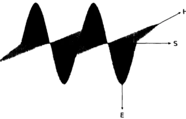
Figure 1-1 shows the magnitudes of the electric and magnetic field for an
electro-magnetic wave propagating in a vaccum. The wave propagates in the direction of the
Poynting vector S:
S=E x H
(1.36)
The Poynting vector defines the direction of energy flow, and its magnitude expresses
the energy flux rate, or intensity of the wave (expressed in units of a"gy e) The magnitude of the Poynting vector is used in Section 3.5 to measure the reflectivity of
dielectric structures. Because the magnitude of the instantaneous Poynting vector is
time-dependent (c.f. how the fields oscillate in figure 1-1), it is often useful to report the time-averaged Poynting vector. The Poynting vector also plays a crucial role in
Poynting's theorems of energy and momentum conservation for electromagnetic fields
and systems of charged particles.
6
I-, H
E
Figure 1-1: An electromagnetic wave propagating in a vaccum. S is the Poynting vector.
1.4 Electromagnetic Waves at an Interface
Maxwell's equations can be used to study what happens to an electromagnetic wave
at an interface between two materials. The study of optics long preceded Maxwell's work and lead to equations useful for describing optical lenses despite the fact that the nature of light was not well understood. The power of Maxwell's equations is demonstrated in that, in addition to describing electrical and magnetic phenomena, they shed light on all optical phenomena, including topics that had been studied before the time of Maxwell such as reflection, refraction, polarization, total internal
reflection, and the Brewster angle.
Figure 1-2 shows an electromagnetic wave being scattered at an interface between materials with indices of refraction nl and n2. The incident wave is partially reflected
and partially refracted (transmitted). Wave interactions at an interface obey the
phase matching condition, which states that the tangential components of the wave
vector, kt, are conserved at a boundary[5]. The wave vector k points in the same
direction as the Poynting vector but its magnitude is the wavenumber,
2.The
phase matching condition, which can be derived from Maxwell's equations, has several
important consequences. First, the kinematics of electromagnetic wave scattering at
an interface can be solved. Conservation of k t for the reflected wave requires that k t
be the same for both the incident and reflected wave and produces the familiar rule that the angle of incidence must equal the angle of reflection. Conservation of k t for
the refracted wave yields Snell's Law:
nlsin(01) =
n
2sin(0
2)
(1.37)
When a wave propagates from a high refractive index material to a low refractive
index material, there will be a critical angle 0c such that when 0c is exceeded, the tangential component of the incident wave vector
k
nlC becomes larger than the total wave vector k in the material with index n2. Thus t cannot be conserved at theinterface for a transmitted wave and the result is total internal reflection. 0c can be found by solving Snell's Law [Eq. 1.37] with 02 = 90°:
0 = sin-
I
n2(1.38)
Another interesting phenomenon occurs when k trans =
k
nc, wherekn
is the valueof the normal component of the wave vector. This condition corresponds to k
nbeing
conserved across the interface. In this case, the Fresnel equations [Eq. 1.41] reveal that there is no reflected wave; all waves are transmitted. The angle at which this occurs is b, the Brewster angle, which can be found by solving the Fresnel equations
for zero reflectivity and employing Snell's Law. Interestingly, the Brewster angle only exists for TM polarized waves (TM is defined in Section 3.2):
Ob = tan-
G'
I = tan-l£
(1.39)_inc1 =
The amount of light that is reflected and refracted when a wave scatters at an
interface can be calculated from the Fresnel equations. F is the reflection coefficient, the ratio of reflected power to incident power, and r is the transmission coefficient, the ratio of transmitted power to incident power. and r are related for a lossless
material such that:
+T
= 1
(1.40)
Figure 1-2: Scattering of an electromagnetic wave at a dielectric interface.
wave. The Fresnel equations for both the TE and TM polarizations (Section 3.2) are shown below: N
Eref 2
rTE =E: n Eon tEref 2 rTM - E77wnc ) FTM = 0neEf
(
_ l_ 2cos(
A2CScos(O1)
2)
Iilcos(Ol)
+ 2 cos(o2)
_ COS(1) - l COS(2) 22coS(01) + ' Cos(02)
(1.41a) (1.41b)E ~
f
1 and E'nC are the amplitudes of the reflected and incident waves, respectively.1.5
Wave Impedance
The reflection and transmission of an electromagnetic wave at an interface can also be thought of in terms of wave impedance. The impedance of a material depends on E and /A, and a difference in impedance between two materials causes electromagnetic waves to be scattered. Such a formulation is useful for understanding the perfectly matched boundary layer described in section 3.4. The wave impedance is the ratio of the transverse electric field to the transverse magnetic field and depends on polarization.
Wave impedance is given as[4]:
ZTM
= cos()1
-(1.42a)
ZTE
= -i=
a1
(1.42b)we cos(O) E
k n is the normal component of the incident wave vector and w is the angular frequency.
For normal angles of incidence, the impedance can be simplified to Z = VI and for angles larger than Oc, the impedance is imaginary[5]. The reflection and transmission coefficients are defined, in terms of the impedance in materials nl and n2 from figure
1-2, as: Z1- (1.43a)
Z + Z2
2Z2r-
2 1 (1.43b) Z2 + IChapter 2
Photonic Crystals
Photonic crystals are periodic arrangements of materials with different dielectric
con-stants that affect the behavior of light. The crystal's geometry exploits the simple
reflection and transmission rules for electromagnetic waves as discussed in section 1.4 in such a way that new and useful optical behaviors are produced. Photonic crys-tals can be used to create perfect dielectric mirrors, light filters and sensors, efficient lasers[8], and waveguides for light. Defects in photonic crystals can be used to trap and control single photons of light[9]. Photonic crystal structures are being used in the development of optical circuits[10], and there has been recent interest in the phenomenon of negative refraction that can be produced with photonic crystals[11].
The study of photonic crystals does not involve more sophisticated concepts than
were developed by Maxwell and others in the 1800's. Although Maxwell could have envisioned photonic crystals, they have only recently been studied seriously because advances in manufacturing techniques have allowed the design of structures on the nanoscale.
Because the wavelength of visible light is about 400nm to 700nm, the structures that create novel behavior must be of roughly the same dimensions. An interesting feature of Maxwell's equations is that they are scalable such that the solution is
inde-pendent of length scale. Thus a solution at one length scale can be scaled and apply to
the same system at any other length scale. Thus when simulating a photonic crystal,
the geometry should be considered rather than the absolute size of the structure.
Figure 2-1: Photonic crystals can be periodic in one, two, or three dimensions. Colors represent materials with different dielectric constants[1].
2.1 The photonic bandgap
Photonic crystal geometries are categorized by their periodicity. Figure 2-1 shows how materials with different dielectric constants may be combined to produce geometries that are periodic in one, two, and three dimensions. The periodicity of the crystal is
an important factor that controls the crystal's photonic properties[12].
One of the most important features of photonic crystals is that they may have
photonic bandgaps. The photonic bandgap is analogous to electronic bandgaps in
semiconductors, except that the electrons from solid-state electronics are replaced by photons. A photonic bandgap can be thought of in a couple of ways. A material with
a photonic bandgap will reflect all light over a frequency range and transmit none of
it, the density of photonic states within the crystal goes to zero in the bandgap, and
the modes within the band gap are evanescent (exponentially decaying).
If a photonic crystal reflects light of any polarization incident at any angle, then it has a complete photonic bandgap. 1D and 2D dielectric structures may have a bandgap in one and two directions respectively, but they will not have a complete 3D
bandgap because there is no periodicity to scatter electromagnetic waves in at least
one direction. 3D photonic crystals are candidates for complete photonic bandgaps,
but because they are much harder to manufacture than their D or 2D counterparts,
they should only be used for applications where a complete bandgap is required. Many dielectric geometries in 1D, 2D, and 3D have been shown to have complete bandgaps for their respective dimensions. Furthermore, many of these structures have been
fabricated and the bandgap confirmed experimentally. Commonly studied photonic
crystal geometries include the quarter-wavelength stack in D, arrays of dielectric
circles, circular voids, or linear veins in 2D, and, in 3D, lattices of voids or dielectric spheres[12]. Other more complex 3D geometries have been discovered[1, 13], including some bi-continuous, triply periodic minimal surfaces that can be manufactured by interference lithography.
2.2 The quarter wavelength stack
The D photonic stack is a simple structure that exhibits a bandgap and that will
be used as the basis for development of more sophisticated 2D and 3D structures in chapters 4 and 5. If the layers of a D photonic crystal (leftmost image, figure 2-1) are chosen such that light of wavelength A travels a distance A/4 in each layer, the structure will have a bandgap at normal angles of incidence and is called a quarter wavelength stack. The bandgap exists because all of the light that is reflected at the
boundaries constructively interferes and emerges from the structure perfectly in phase.
Consider the phase of a plane wave as it penetrates the structure and is partially
reflected at each interface. The light that emerges from the quarter wavelength stack has travelled an integer multiple of A/2 in each layer, because it must pass through the layer completely at least twice - once when incident and once when reflected. Additionally when light is travelling in a material with low dielectric constant and is reflected by a material with higher dielectric constant there is a phase change of ir. The combined effect of these observations is that all of the light is eventually reflected
and exits the structure in phase, producing a bandgap.
2.3 Calculating photonic bandgaps
The calculation of a photonic bandgap requires solving Maxwell's equations for a
dielectric structure. Frequency domain and time domain algorithms are two different
advantages and disadvantages.
The frequency domain approach involves solving Maxwell's equations for eigenval-ues and eigenfunctions, analogous to computing the Bloch wave function in quantum mechanics. It is frequency domain because it determines the wave mode eigenfunc-tion H (r) for a specific frequency w that is directly related to the eigenvalue (w/c)2. Maxwell's equations are decoupled to produce a Schrodinger-like equation that can be solved for eigenfunctions and eigenvalues[12]:
x
(
x H(r) =
(r)
(2.1)
The frequency domain is appropriate for determining dispersion relations for photonic
crystals and for analysis of the photonic band structure, which describes how the wavelength of a propagating wave varies with frequency.
The time domain solution is obtained by iterating Maxwell's equations through
time on a spatial grid. The state of the system is known at a specific time, but not
necessarily for any specific frequency. Time domain simulations allow for analysis of where fields concentrate in the system and are useful for measuring transmittance and decay times. Time domain simulations, unlike frequency domain simulations, are not restricted to solving for periodic structures because of the development of
absorbing boundaries that effectively create a computational domain extending to
infinity. Thus any arbitrary, finite system can be simulated. Unfortunately, unlike frequency domain simulations, time domain simulations do not scale well with changes in grid resolution or system size. Also, in the time domain, closely spaced modes may not be distinguishable if the frequency resolution is not high enough. Such a
resolution problem will not happen in the frequency domain because different bands
are represented by different eigenvalues.
An advantage of the time domain is the ability to solve for a system's response
to all frequencies from just one simulation. In the frequency domain for comparison,
a new simulation must be run for each frequency to be investigated. This ability
is possible in the time domain because the time domain and frequency domain are
related via Fourier transforms. A measurement of the response over all frequencies can be achieved by measuring the system's response to an impuse function, which contains all frequencies. As described by Weaver [14], the function y(x) that describes the response of the system to an input function f(x) is given by the convolution of
f(x) with h(x), the response of the system to the impulse function:
Chapter 3
The Finite-Difference Time
Domain Approach
3.1
Finite Differences
FDTD simulations use the method of centered finite differences to solve differential equations numerically on a grid. At a point i,j,k in space, the derivatives in the
x-direction are approximated from the values at neighboring points using centered
differencing:
u _ Ui+l,j,k - Ui-lj,k
+
[(AX) 2](3.la)
,Ox
2Ax
0
2U Ui+lj,k - 2Uij,k + Ui.l,j,kOx2 (AX)2
where Ax is the distance between gridpoints in the x-direction. Equations for
deriva-tives in other directions have the same form. This method is "centered" because one
point on either side of
Ui,j,kis used to compute the derivative. The method is only an
approximation of the actual derivative, because the derivative is defined in the limit that the grid spacing goes to zero. The amount of error for centered differencing is
proportional to (Ax)
2, and thus it is second-order accurate. Although the
differenc-ing scheme has been presented for spatial derivatives, it will also be used to compute temporal derivatives and will provide second-order accuracy in time.
Transverse Magnetic Mode (TM)
(a) (b)
Figure 3-1: There are two independent polarization modes, TE and TM, which occur in 2D electromagnetic simulations.
3.2 TE and TM Modes
Three vectors are needed to find a solution to Maxwell's curl equations because the
cross product in the equations relates three orthogonal vectors. For simulation of a
2D structure there are two possible polarizations to choose from when assigning fields to the 2D computational grid. These two modes are illustrated in figure 3-1, where it can be seen that either H., Hy, and Ez or E, Ey, and H must be chosen as the fields
to simulate. The modes are called transverse electric (TE) and transverse magnetic
(TM) respectively. Interestingly, it can be derived from Maxwell's equations that the two modes are uncoupled and will not always produce the same behavior. There is disagreement on the naming of the different modes. Joannopoulos, for instance, defines the two modes exactly opposite to the definition used in this work[12].
In terms of the Poynting vector, the two modes represent the only two possible polarizations for a 2D plane wave. Recall that the Poynting vector S is the cross
product of the E and H fields. The Poynting vector can be rotated about its axis
such that its direction and magnitude remain constant but E and H are rotated in
the plane normal to S. The different orientations of E and H represent different
polarizations. Polarizations in 3D do not fit into these two categories, and the possible
polarizations are related to the point group symmetry of the structure.
2D Computational Domain 2D Computational Domain
Transverse Electric Mode (TE)
z
(ij
Figure 3-2: The 3D Yee grid[2].
3.3 The Yee Algorithm
In 1966, Kane Yee developed a simple, efficient, and powerful algorithm for numer-ically solving Maxwell's equations on a finite grid[15]. His algorithm is still widely used today. Yee used a centered differencing scheme [Eq. 3.1a] to solve Maxwell's equations [Eq. 1.31] for both the electric and magnetic fields in space and time. Mod-eling both fields produces robust solutions and allows for the modMod-eling of electric and
magnetic material phenomenon.
A Yee grid for a two dimensional TE mode simulation is illustrated in figure 3-5, and a 3D gridding is shown in figure 3-2. In the Yee grid, the magnetic and electric fields are offset from each other by 1 of a gridpoint. This allows Yee's gridding scheme to implicitly solve Gauss' divergence laws [Eq. 1.31c, 1.31d] because each E field point is surrounded by a loop of H field points, and each E field point is surrounded by a
loop of H field points. Thus the scheme naturally captures the ideas of Ampere's and
Faraday's Laws where flux of an electric or magnetic field through a point induces a loop of either electric or magnetic field, and evolution of Maxwell's equations through time is achieved by employing only the time-dependent curl equations [Eq. 1.31c,
The Yee algorithm uses a leapfrog timestepping approach, where each timestep is
divided into two parts. In the first half of the timestep the electric field is updated.
In the second half, the magnetic field is calculated using the just updated electric field values. This approach is explicit and second-order accurate in time because it is centered in time. Were forward or backward time differencing used, the solution would only be first-order accurate in time. The Yee discretization of Maxwell's curl equations [Eq. 1.31a, 1.31b] is shown below for the x direction:
D (i
+
1,
)-Dz
2(i
+
2,
, k)
Hn(i
+ j + k) -Hn(i
+ 1,
-At
Ay
Hy(i
+ 1,
j, k +
Hy(i
+ 1,
j, k
Az
B~n+1 +(i,
j+
E
(iJ+
1)
+
i
, k)
At
Az
E+
(i,
j
+ 1,
k
+
) - E+
2(i,j,k
+
2)
Ay
The equations for the y and z directions are similar in form. The 2D equations for both the TE and TM mode can be found by eliminating the k index and setting the appropriate fields equal to zero. For TE mode Ex = Ey = 0, and for TM mode
H = H = 0.
3.4 Boundary Conditions
An absorbing boundary called a perfectly matched layer, or PML, was used in the
simulations presented below. This particular boundary condition was developed by
Berenger[16]. The PML allows for simulation of an infinite computational domain
by attenuating the electromagnetic waves at the boundary with minimal reflection.
Terminating the computational domain or introducing an artificial boundary causes
the electromagnetic waves to be reflected back into the simulation and inhibited
the initial use of FDTD for electromagnetic simulations. Several other absorbing
boundary algorithms have been proposed, but Berenger's method remains one of the
most accurate, and also damps waves at angles of incidence other than the normal
angle.
Berenger's PML exploits the fact that if and are chosen in two different materials such that the impedance Z (as described in section 1.3) in each material is
the same, there will not be any reflection at the interface. Furthermore, the waves
can be made to decay with the use of complex values for p and e. Berenger's method also involves a field-splitting modification of Maxwell's equations for the gridpoints in the PML boundary layer that is necessary to decay the waves. An implementation of the PML coded by Sullivan was incorporated into the developed code[17].
3.5 Computational Setup
The grid layout used to calculate reflectivity band diagrams of dielectric compos-ites using the finite difference method is illustrated in figure 3-3. A unidirectional plane wave is generated from a line source, and allowed to propagate through a
vac-cum toward a dielectric structure. The plane wave then interacts with the dielectric
structure and is partially reflected and partially transmitted. The amplitude of the
reflected and transmitted waves changes, but their frequencies do not. The reflected
and transmitted waves are measured at the indicated locations in figure 3-3 after the
system has reached steady state. The reflected signal must be measured behind the
unidirectional source where only the scattered field exists; both the incident and
re-flected waves exist in the region between the source and the structure. Measurement of the reflected or transmitted wave involves computing the time-averaged power over a region of gridpoints. The power of an electromagnetic wave is the magnitude of the Poynting vector,
E
, averaged over time. The reflectivity is the ratio of aver-age reflected power to averaver-age incident power, which is the same as the ratio of thetime-averaged Poynting vectors. Reflectivity can be expressed as:
r
=
_
2
(33)
where E r is the electric field of the reflected wave and Ei that of the incident wave.
nr and ni are the number of gridpoints over which 1E is summed in the reflected and incident regions respectively (i.e. spatial averaging). The angled brackets denote time averaging. It should be noted that because = for electromagnetic waves, the reflectivity could also be measured in a similar manner using the magnetic
field.
The length of time for which the reflected power is averaged must be constrained to correspond to the passage of an integer number of wavelengths. In this study, 24
periods was found to be sufficient to produce stable results, and transmitted power r
was measured instead of reflected power. r was found from the relationship F -r = 1, which holds for the perfect dielectrics (i.e. a = 0) that were simulated. Measuring the
transmitted power produced bandgaps that accurately matched accepted results[18]
and transmitted power was measured when calculating the bandgaps in the
appen-dices. Measuring reflected power directly produced results that occasionally deviated slightly from the accepted results. The error was not large, and it is possible that
there was an interaction between the reflected waves and the unidirectional source.
Although it is supposed to be transparent, the unidirectional source may have slightly
interacted with reflected waves.
3.6 Parallelization
The software developed was designed to support massive parallelization. The FDTD
approach is easily parallelized for solving general finite difference problems across multiple CPUs. FDTD simulations were parallelized using a divide and conquer approach illustrated in figure 3-4a. This approach is well suited for FDTD because
Absdrbing Boundary " Dielectric Structure I I I I I I I
~~I
m Me~~~I~u I | Moncilron trncmicinn I - Absorbing oundary …--- --- Periodic BoundaryFigure 3-3: The computational setup for calc(ulating the reflectivity band diagram of a dielectric structure.
the central differencing scheme used requires only that the immediate neighbors of a gridpoint be known in order to advance that gridpoint in time. Thus the large grid illustrated in figure 3-3 can be divided into many smaller subgrids illustrated in figure 3-4a, which can be evaluated in parallel by separate processors.
When the original grid is divided into subgrids, each gridpoint at the boundary
of two subgrids will be missing neighbor that it needs and which is stored on an adjacent subgrid, possibly located in the nemory of a different CPU. Thus to insure that every gridpoint can be evallated, each subgrid must exchange boundary gridpoints with its neighboring subgrids at the end of each timestep. Exchange of
boundary layers is illustrated with arrows in figure 3-4a. The exchange of boundaries must be completed at the end of each timrestep and before the next tirnestep can be evaluated.
The division of the original large grid ito several smaller grids for parallelization was designed to be as transparent ats possible for future progralmers. Parallelization
I · _~~~~~~~~~~~~~~~~~~~~~~~~~~~~I
Al
is implemented for an arbitrary number of processors provided by the user at runtime,
and the user does not have to worry about how to divide and distribute the work
-the division is performed automatically. The software contains logic for choosing how to divide up the initial large grid into smaller subgrids. The software analyzes the dimensions of the grid to compute which direction to divide it. It is advantageous to divide the grid in such a way as to minimize the size of the boundaries between subgrids because these boundary values will be exchanged, possibly over an ethernet connection which may cause a bottleneck. Each subgrid is a C++ object that keeps
track of its neighboring subgrids and therefore knows its absolute position in the
overall grid. Items that the programmer places in the grid, such as dielectric struc-tures, plane-wave sources, or measuring points can then be referenced using absolute
coordinates and not the relative coordinates for the specific subgrid that the objects
exist in. Additionally, objects can span multiple subgrids without needing special
attention.
Parallelization was implemented using the Message Passing Interface (MPI) which is a standard language for writing parallel and distributed programs. Because MPI
is a communication protocol rather than an implementation, it does not require any
specific hardware, operating system, or compiler and works efficiently for many
com-puter configurations. CPUs used for parallel computation can be virtual, located
on a multi-processor system using shared memory, or located on computers that are
networked together.
Parallelization provides two important advantages for electromagnetic FDTD
sim-ulations. First, it provides a measurable speed increase. Figure 3-4b shows that the
running time of a 2D FDTD simulation is improved as more CPUs are added. The
second advantage of parallelizing FDTD simulations is that it eliminates a potential
memory bottleneck. With a single processor simulation, the size of the simulated
system is limited by the size of a grid that can fit in the computer's memory without causing a memory overflow. The maximum size of a parallel grid is related to the sum of the memory in every computer being used to solve the problem. If the system becomes too big for one node in the cluster, adding more computers will make the
Dielectric Structure
Effect of Parallelizing a 2D FDTD Simulation of 450,000 Gridpoints
CPU 350 300 u 250 CPU 2 - 200 a: 150 100 50 CPU 3
[ '&. A'barbing~Bnd&r"':¥-I Number of processes
(a) (b)
Figure 3-4: An increase in performance is observed with a parallelized FDTD simula-tion. A point of diminishing returns is reached for a large number of processors such that adding an additional processor does not significantly affect the running time of
the simulation.
problem solvable. In this way it's possible to solve problems on a cluster of computers that are much too large to solve on any one computer in the cluster alone. Addition-ally, 32-bit memory addressilng limits the size of a grid on a single CPU to 4Gb. With this parallelization scheme, the 4Gb limit is avoided on 32-bit machines because the parallelization scheme effectively implements a distributed memory architecture.
3.7 Creating a source with the total/scattered field
formulation
A efficient unidirectional, periodic, angled source was derived for use in FDTD
electro-magnetic simulations. The source was developed by modifying the
total-field/scattered-field boundary as described by Taflove and HagIless[2]. This approach is based on the idea that for an electromagnetic plane wave interacting with a dielectric, the total
V• '1: ts~~~~~~s:6~_ Measure reflectance Plane-wave source A ' . ~' mr---- wm __-m.___ Measure transmission Measure transmission I, "E [ i I , I ... '1 .AA -
~
~~~I
I . 1 I\ _ __ __ __ __ __ _ _ __ __ __ __ __ ---I . " Y " " '""'wave is the sum of the incident and scattered parts:
E
total =E
inc +E
scat(3.4a)
H
total =H
inc + H scat(3.4b)
In general, an FDTD electromagnetic simulation will evolve the total field, al-though it is often the scattered field that is desired for analysis. The incident field is known because it is defined by the programmer as some time-varying field: often a plane wave or Gaussian pulse. The scattered field can only be found by subtracting
the incident field from the total field. The simplest way to calculate the scattered
field is to run two simulations. One simulation contains the dielectric structure and
is used to calculate the total field. The second simulation simulates the incident
field on a grid of identical dimensions, but with the dielectric structure replaced by
vacuum (n = 1.0). The scattered field is found at each timestep by subtracting the
incident field from the total field. Although this approach is conceptually simple, it
is inefficient. Twice the number of gridpoints and memory are required, resulting in the simulation being slow and possibly causing a memory overflow. If the simulation is run in parallel, twice as many boundary values must be passed between subgrids.
The total/scattered field boundary formulation provides an efficient way of
sepa-rating the scattered field from the total field and allows for the introduction of
non-physical unidirectional transparent sources. A unidirectional source is non-non-physical because any line or plane of oscillating fields in a physical system will produce a wave that propagates away from the source in all directions. Unidirectionality is effectively achieved by cancelling out the propagation of the wave in one direction, creating a
total/scattered field boundary.
Figure 3-5 illustrates the formulation of the total/scattered field for TE polariza-tion. A similar figure applies to the formulation for TM. The formulation corrects
inconsistencies that develop at the boundary between a total and scattered field. Such
a boundary is illustrated with white and shaded regions in figure 3-5. The boundary
is located between gridpoints jb and jb + 1/2. Application of the Yee equations
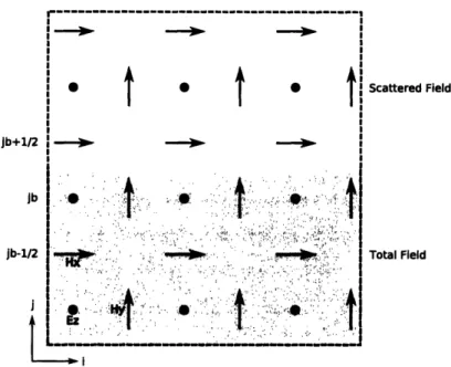
re-jb+1/2 jb Jb-1/2 A _ A_ A Scattered Field Total Field I
Figure 3-5: A Yee gridding of the electric and magnetic fields for a 2D TE mode
electromagnetic simulation. The total/scattered field formulation is used to create a
unidirectional, transparent source.
veals that the calculation of Ez points at jb and Hz points at jb+ 1/2 are inconsistent
because one point from the scattered field and one point from the total field are used. The inconsistency can be resolved by appropriately adding or subtracting the incident field, which is known by the programmer, after each inconsistent calculation has been made. The correction terms are:
Ezn+(i,jb)
=
En+2(i,jb)-
---
Hin(ijb+-)
(3.5a)
1
1 A t n+,H'+l(i, jb+ )
= Hn+l(i,
1jb
) +
E
(i,
jb)
(3.5b)
2 2eA
'x
zinc,,3.8 An Angled Source
The general form of a 1D travelling wave with wavelength A and period T, travelling in the x-direction is:
y = sin(kx - wt)
(3.6)
, .· I ''*
.
. :
:
.
?
<
.
..
~ ::::~:t~::,,::
2
.I
:,:,
i,t
H
a
' ': ':
'I'
:
:
' :
'
',
,,
:,.
zt .: L · ': ·· : , ·:·. ,·1. : : * i$
_ I:* e ·n~..: _· ··?,,---where k = 2 is the angular wavenumber, x is the position, w = 2 is the angular
frequency, and t is time. As time progresses, the amplitude at each x position changes and the wave is observed to propagate. In the case of electromagnetic waves propa-gating through a vacuum, the velocity at which the wave propagates is the speed of
light, c.
In 2D and 3D FDTD electromagnetic simulations, a periodic plane wave can be generated from a line or plane of discrete gridpoints that oscillate in phase, as illustrated in figure 3-3. A line of oscillating fields in 2D and a plane in 3D generate a plane wave because, according to Huygens' principle, all points on a wavefront serve as point sources of spherical secondary wavelets. After a time t, the new position of the wavefront will be that of the surface tangent to these secondary wavelets[19].
Each point on the source line or plane contributes a spherical wavefront to the tangent
surface of a plane wave. However, creating an angled incident wave on a square FDTD grid is troublesome. A simple solution would be to place the source line or plane at an angle relative to the grid, but the plane wave source must be periodic so that it is compatible with periodic boundaries. If the source is simply inclined relative to the grid, the source is not periodic because the source is not continuous across the
periodic boundaries. The same periodicity argument can be made for keeping the
source fixed and simply rotating the dielectric structure - the rotated structure will
not be periodic. Placing the source at an angle relative to the grid introduces aliasing
as well because an angled line of points cannot be exactly represented on a square grid - the sampling of points along the line will be non-uniform, and the nonuniformity will depend on the angle of the source. Low inclination angles would be particularly troublesome.
If the incident field varies periodically in time along the x-direction of the source line, an angled plane wave will be generated. Because the systems being investigated are periodic in the x-direction, the variation of the field in that direction must also be periodic such that an integer number of wavelengths fits along the x-axis. The consistency rule is:
~~~~~~~~~I
I I I X=X\sin(e) I I * I I I k it
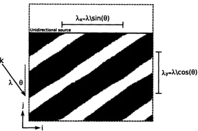
Figure 3-6: Generation of a unidirectional angled plane wave with wavelength A and angle 0.
where A is the wavelength of the angled wave generated, m is an integer and n is
the number of gridpoints in the x-direction. If the condition is not met, the angled
wave will not be periodic and will be inconsistent with the boundary conditions. Figure 3-6 shows a unidirectional, periodic, angled plane wave source for a 2D
FDTD simulation. The wavelengths in the x and y directions are labeled as A, and
A. An equation that describes the amplitude of the 2D plane wave as a function of position (analogous to Eq. 3.6) is:
y = sin (kx i + kj - wt)
(3.8a)
= sin(
i+ -
ct)
(3.8b)
y = sin (2 (i sin() + j cos() -c t))
(3.8c)
When substituted into the total/scattered field equations (Eq. 3.5), the equations
for an angled 2D plane wave for TE mode become:
1( )

![Figure 3-2: The 3D Yee grid[2].](https://thumb-eu.123doks.com/thumbv2/123doknet/14733842.573679/35.918.297.645.103.413/figure-d-yee-grid.webp)