Development of Vertical Bulk Gallium Nitride Power Devices by Ayrton D. Muñoz
S.B, Electrical Engineering M.I.T. 2017 Submitted to the
Department of Electrical Engineering and Computer Science in Partial Fulfillment of the Requirements for the Degree of Master of Engineering in Electrical Engineering and Computer Science
at the
Massachusetts Institute of Technology September 2019
©2019 Ayrton D. Muñoz. All rights reserved.
The author hereby grants to M.I.T. permission to reproduce and to distribute publicly paper and electronic copies of this thesis document in whole and in part in any medium now known or hereafter created.
Author:
Department of Electrical Engineering and Computer Science September 18, 2019
Certified by:
Tomás Palacios, Professor September 18, 2019 Accepted by:
Development of Vertical Bulk Gallium Nitride Power Devices by
Ayrton D. Muñoz
Submitted to the Department of Electrical Engineering and Computer Science on September 18, 2019, in partial fulfillment of the
requirements for the Degree of
Master of Engineering in Electrical Engineering and Computer Science
Abstract
Gallium nitride (GaN) is a promising material for power electronics due to its outstanding properties, such as high critical electric field and large bandgap. Despite its superior intrinsic properties, fabrication processes and technology for vertical GaN power electronics is still not as mature as in conventional ma-terials. This thesis covers three aspects of vertical power devices on bulk GaN to increase their reliability and performance. The first is the breakdown behavior of GaN under high electric fields. Vertical Schottky diodes with multi-finger anodes are simulated, fabricated and characterized. Evidence of impact ionization and signs of avalanche breakdown are shown. The second aspect is scalable fabrication technologies for vertical power FinFETs. Key processing stesps are refined and demonstrated on large-area devices. The final topic covered is GaN superjunction (SJ) technology in the context vertical power FinFETs. The SJ FinFET concept is first introduced then an underutilized method for p-type doping GaN is explored as an alternative to conventional p-type regrowth and ion implantation. Finally, the proposed GaN SJ FinFET is investigated with simulations. Various standard SJ parameters are optimized and a novel electric field management technique is proposed.
Thesis Supervisor: Tomás Palacios Title: Professor
Acknowledgements
First, I would like to thank Professor Tomás Palacios for his guidance and support. I am grateful for his excitement about pursuing ambitious projects and the many insightful discussions we have had.
I would also like to thank the members of the group. In particular I would like to thank Yuhao Zhang and Daniel Piedra for their mentorship, Joshua Perozek for sharing his expertise in fabrication and Hengyu Wang for the extensive help with the simulations. I would also like to thank Elaine McVay, Marek Hempel, Pao-Chuan Shih, Qingyun Xie, Ahmad Zubair, Mengyang Yuan, Nadim Chowdhury, Yuxuan Lin, Mantian Xue and the rest of the group for all their support and creating an exciting, collaborative environment.
The fabrication work in this thesis would not have been possible without the help of the the Microsystems Technology Lab at MIT. I am grateful to the MTL research staff, particularly Dave Terry, Bob Bicchieri, Dennis Ward, Eric Lim, Donal Jamieson Kurt Broderick, Tim Turner and Paul Tierney, for their effort in maintaining the fabrication tools. I would also like to thank the administrative staff, in particular Joe Baylon, for always ensuring that things ran smoothly.
I would also like to extend thanks to the various collaborators who contributed to the work in this thesis. Specifically Xiang Gao at IQE and Richard Molnar at Lincoln Labs for growing our wafers, Zhihong Liu for his help with ion implantation and Garrett Schlenvogt and Thomas Jokinen at Silvaco for help with device simulation.
This research was funded by the ARPA-E SWITCHES program managed by Dr. Isik Kizilyalli. Finally I would like to thank my friends and family for their endless support.
Contents
1 Introduction 15
1.1 Power Semiconductor Devices . . . 15
1.2 Wide Bandgap Semiconductors . . . 17
1.2.1 Baliga Figure-of-Merit . . . 18
1.3 Challenges for Gallium Nitride Power Devices . . . 19
1.3.1 Lack of Avalanche Breakdown . . . 19
1.3.2 Scalable Fabrication Technology for High-Performance Vertical Transistors . . . 20
1.3.3 Exceeding Unipolar Limits with Superjunction Structures . . . 21
1.4 Scope of this Thesis . . . 22
2 Avalanche Breakdown in GaN Schottky Diodes 23 2.1 Impact Ionization and Physics of Avalanche Breakdown . . . 23
2.1.1 Avalanche Breakdown in Power Electronics . . . 23
2.1.2 From Impact Ionization to Avalanche Breakdown . . . 26
2.1.3 Indicators of Avalanche Breakdown . . . 27
2.1.4 Impact Ionization Rates in GaN, SiC and Si . . . 28
2.1.5 Designing Avalanche-Capable Power Devices . . . 30
2.2 Schottky Diode Design and Simulation . . . 31
2.2.1 Schottky Diode Design . . . 31
2.2.2 Simulation Methodology . . . 32
2.2.3 Simulation Results . . . 35
2.3 Device Fabrication . . . 37
2.3.1 Wafer Structure . . . 37
2.3.2 Reducing Leakage Current . . . 39
2.3.3 Contact Deposition . . . 42
2.4 Electrical and Optical Characterization . . . 43
2.4.1 Measured I-V Characteristics . . . 43
2.4.2 Reverse Bias Electroluminescence . . . 45
3 Fabrication of Vertical GaN Power FinFETs 48
3.1 Vertical Power Transistors . . . 48
3.1.1 Introduction . . . 48
3.1.2 Vertical GaN Transistor Structures . . . 49
3.2 Fabrication Technologies . . . 51
3.2.1 Main Fabrication Steps . . . 51
3.2.2 Fin Patterning Process . . . 52
3.2.3 Gate Etch Process . . . 57
3.2.4 Gate Oxide Etch Process . . . 62
3.3 Conclusion . . . 65
4 Design and Simulation of GaN Superjunction FinFETs 66 4.1 Superjunction Technology . . . 66
4.2 P-type Doping GaN by Diffusion . . . 68
4.3 GaN Superjunction FinFET Simulation . . . 71
4.3.1 Charge Balance . . . 73
4.3.2 Reducing Electric Field Peaks . . . 75
4.4 Conclusion . . . 78
5 Conclusions 79
Appendices 81
A Silvaco Atlas Code for Vertical Multi-Finger Diodes 82
List of Figures
1.1 Electric field (left) and charge density (right) profiles for a uniformly doped drift region. . . . 16
1.2 Minimum drift region width (left) and maximum doping density (right) for a given breakdown voltage in GaN using Ec=3.5 MV/cm and εr=8.9. . . 17
1.3 BFOM limit for unipolar devices for relevant materials using the parameters listed above. . . 19
1.4 Lateral MOSHEMT structure (left) and vertical MOSFET structure (right) on bulk GaN. . . 21
2.1 Flyback diode D clamping the inductive load L driven by M . . . 23
2.2 Reverse-bias I-V characteristics representative of an avalanche-capable device. . . 24
2.3 Waveforms showing the drain voltage clamping (black) when the inductor current quickly drops (blue). . . 25
2.4 Parametrized impact ionization coefficients for bulk GaN, SiC and Si from photodiode mea-surements (left) and Monte Carlo calculations of bulk GaN (right) [28]. . . 30
2.5 Equations 2.7 and 2.8 for ND=7e15 cm−3, φbi = 0.88V and various values of W . This simple model breaks down when the electric field becomes high enough for a significant amount of impact ionization to occur. This point is marked by the dashed red line for GaN. . . 32
2.6 Simplified device structure used in Atlas simulations. . . 33
2.7 Simulated electric field profile for upper portion of the device in Figure 2.6. . . 33
2.8 Impact generation rate profile for the same portion of the device shown in Fig. 2.7. . . 34
2.9 Simulated reverse bias IV characteristics for a multi-finger device. . . 35
2.10 "U-shaped" electric field that occurs due to buildup of charge in the drift region during avalanche. The device considered here has two highly doped layers between the drift region and the cathode, but nearly identical behavior occurs for the simplified model shown in Figure 2.6. . . 36
2.11 Variation in simulated avalanche breakdown voltage with spacing between fingers. . . 37
2.12 Original wafer structure (left) and target device structure (right). . . 38
2.13 SIMS data from original wafer (left) and C-V Schottky diode characterization. . . 38
2.14 Defects protruding from surface after a 3 µm etch. . . 39
2.15 Electric field profile in a Schottky diode with a 2 µm mesa and 6 µm drift region at 100 V (left), 200 V (center) and 300 V (right). . . 40
2.16 Electric field profile in a Schottky diode with a 5 µm mesa and 3 µm drift region at 100 V
(left), 200 V (center) and 300 V (right). . . 40
2.17 Various GaN test samples after etching in hot TMAH. . . 41
2.18 Hexagonal mesa with A plane exposed. . . 41
2.19 Mask used to pattern the multi-finger Schottky diode anodes. . . 42
2.20 Measured reverse bias characteristics showing sharp current increases in different multi-finger devices. . . 43
2.21 Cross section and electric field profiles representative of the standard control diodes (left) and the multi-finger diodes (right). Compared to the control diodes, multi-finger diodes have many more points where the electric field exceeds 3 MV/cm and appreaciable levels of impact ionization can be seen in GaN. . . 44
2.22 Measured reverse bias characteristics for circular control diode and a multi-finger diode with-out the sharp current increase. . . 45
3.1 Vertical MOSFET structure on bulk GaN. . . 49
3.2 Vertical CAVET structure on bulk GaN. . . 50
3.3 Vertical Power FinFET device and wafer structure. . . 51
3.4 Main fabrication steps for vertical power FinFETs. . . 52
3.5 Standard lift-off process for patterning hard mask to etch fins. (a) PMMA is spincoated onto the wafer. (b) Ebeam lithography is used to pattern the PMMA. (c) A Ni hard mask is evaporated onto the wafer. (d) The remaining PMMA is washed away with hot NMP removing the excess Ni. (e) The GaN is dry etched with the Ni mask used to define the fins. (f) The Ni mask is removed with piranha. . . 53
3.6 Metal-first process for patterning hard mask to etch fins. (a) A metal hard mask is deposited onto the wafer followed by spincoating with photoresist. (b) Ebeam lithography is used to pattern the photoresist. (c) The metal hard mask is etched with photoresist used to pattern the metal. (d) The remaining photoresist is removed in acetone or NMP. (e) The GaN is dry etched with the metal hard mask used to define the fins. (f) The metal hard mask is removed by wet etching. . . 54
3.7 Etched GaN fins defined by the Ni wet-etch process. . . 55
3.8 Top view of HSQ fins on Cr. . . 56
3.10 Process flow for the timed photoresist etch to pattern the field oxide. . . 58
3.11 Opposite ends of a 1.5 mm wide power FinFET fabricated with the timed photoresist etch process for the gate stack. . . 59
3.12 Improved gate etch process. (a) The gate stack (Al2O3/Mo/Al) is deposited conformally. (b) SiO2is deposited conformally. (c) The SiO2is etched back to expose the gate stack and the Al is wet etched. (d) Photoresist is spincoated on. (e) The photoresist is etched back to expose the gate stack. (f) The exposed Mo is dry etched and the photoresist is removed in hot NMP. 61 3.13 Key points in the improved gate etch process. . . 62
3.14 GaN fins after Al2O3removal on 0.5 mm2devices. . . 63
3.15 GaN fins after Al2O3removal on 2.25 mm2 devices. . . 64
4.1 Schematic of a superjunction structure for a diode. . . 66
4.2 SIMS results from diffusing sputtered MgO into c-plane GaN at 900◦C for 3 hours. . . 69
4.3 Optical microscope image after diffusing Mg into GaN with an AlN cap layer. . . 70
4.4 Optical microscope image after removing the Mg and AlN cap layer. . . 70
4.5 SEM images of pits and non-uniformity after removing the Mg and AlN cap layer. . . 71
4.6 SIMS results from diffusing sputtered Mg (100 nm) into c-plane GaN at 900◦C for 1 hour and 3 hours. . . 71
4.7 Proposed superjunction structure and simulated half-cell. Trench width = 4 µm, trench height = 7 µm, fin width = 180 nm, fin height = 1 µm, mesa width = 2.5 µm, P-pillar width = 500 nm, P-pillar height = 6 µm. . . 72
4.8 Breakdown voltage as a function of charge inbalance by varying the p-type dopant concen-tration. The maximum breakdown voltage is reached when the charge is balanced at NA = 1.5e17 cm−3. . . 74
4.9 The BFOM as a function of α by varying the n-type doping. Note that while VB in these sweeps is the ideal value, the channel resistance is a non-negligible component of Rspleading to a more pronounced effect for taller pillars. . . 75
4.10 Electric field profile in a SJ FinFET with 8 µm tall pillars biased at -1000 V. The plot on the right is the electric field along the dashed, red cutline through the center of the fin. . . 76 4.11 Electric field profile in a SJ FinFET with 8 µm tall pillars biased at -1400 V. Here the entire
4.12 Zoomed-in electric field profile in a SJ FinFET. Note that the cutline goes from the edge of the p-type pillar to the center of the n-type pillar. . . 77 4.13 Electric field profile along the center of a fin in the laterally-shifted fin structure compared to
the standard SJ FinFET. Both devices have 8 µm tall pillars and are biased at -1200 V. . . . 78
List of Tables
1.1 Critical electric field, bandgap relative permittivity, electron mobility and Baliga figure of merit (normalized to Si) for relevant materials [36] [30]. . . 18
Chapter 1
Introduction
1.1
Power Semiconductor Devices
Power semiconductor devices, such as metal oxide semiconductor field effect transistors (MOSFETs), insu-lated gate bipolar transistors (IGBTs) and high-electron mobility transistors (HEMTs) are used to control the flow and conversion of electric power. These high-power switches are used in a wide variety of applica-tions such as data centers, electric vehicles, electrical grids, etc. In the off-state, high voltages can be applied between the two terminals with minimal current leaking through. During on-state operation, devices allow large currents to flow between two terminals with minimal resistance to prevent significant power dissipation. Although the on-state resistance can be decreased by increasing the device’s active area, this also increases capacitance and switching power losses. Designing power devices involves a tradeoff between the maximum breakdown voltage (VB) and the minimum specific on-state resistance (Rsp).
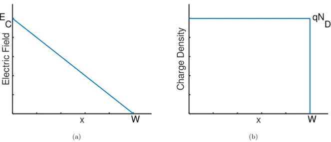
In devices with a unipolar drift region, reaching a target VB requires a minimum width and maximum
doping level1. Assuming a linear electric field profile in the drift region, as shown in Figure 1.1 (a), with
peak Ec at breakdown, the drift region width is found to be
(a) (b)
Figure 1.1: Electric field (left) and charge density (right) profiles for a uniformly doped drift region.
VB = Z E(x)dx = Z W 0 Ec(1 − x W)dx = EcW 2 (1.1) W = 2VB Ec (1.2)
Assuming the drift region is fully depleted at breakdown and using a uniform doping profile ND, Gauss’s
law gives the required doping
Ec= Z ρ(x) ε dx = Z W 0 qND ε dx = qNDW ε (1.3) ND= εE2 c 2qVB (1.4)
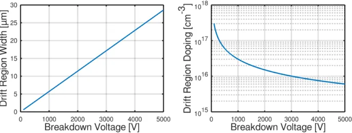
This minimum drift region width and maximum doping, which are shown in Figure 1.2 for GaN, vary significantly between semiconductors as they depend on material properties.
Figure 1.2: Minimum drift region width (left) and maximum doping density (right) for a given breakdown voltage in GaN using Ec =3.5 MV/cm and εr=8.9.
Since the drift region resistance is typically the dominant component of the total resistance in well-designed devices, the ideal Rsp can be found using W and assuming the carrier concentration n equals the
doping ND Rsp= W σ = W qµnn ≈ W qµnND (1.5) Rsp= 4VB2 εµnEc3 (1.6)
This relationship between Rsp and VB highlights the importance of materials with the ability to sustain a
high electric field.
1.2
Wide Bandgap Semiconductors
Wide bandgap semiconductors have a large gap between the valence band maximum and the conduction band minimum while maintaining high conductivity. This class of materials is a promising direction for next-generation power electronics due to the high electric fields they can withstand. This characteristic is typically quantified by a phenomenological parameter called the critical electric field Ec. Although the value
1.2.1
Baliga Figure-of-Merit
As fabrication technologies advance, commercial power semiconductor switches have begun to approach fun-damental limits imposed by conventional materials like silicon (Si). As a result, materials such as gallium nitride (GaN), silicon carbide (SiC), aluminum nitride (AlN), gallium oxide (Ga2O3) and others are being
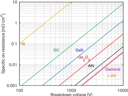
considered as alternatives for next-generation power switches. A common way to compare the limits of different materials is Baliga’s figure of merit (BFOM) [2] which is defined as
BF OM = εµnE3c (1.7)
Although the BFOM only considers conduction power losses in unipolar devices, it provides a good starting Material Ec (MV/cm) Eg (eV) εr µn (cm2/Vs) BFOM (normalized)
Si 0.3 1.12 11.7 1400 1.00 4H-SiC 2.0 3.26 9.7 700 122.82 GaN 3.5 3.44 8.9 900 776.53 β-Ga2O3 8.0 4.85 10 300 3473.07 AlN 11.7 6.1 9.1 425 14005.87 Diamond 10 5.47 5.5 2000 24872.24 c-BN 15 6.4 7.1 500 27090.95
Table 1.1: Critical electric field, bandgap relative permittivity, electron mobility and Baliga figure of merit (normalized to Si) for relevant materials [36] [30].
point for evaluating the potential of different materials for high-power switches operating at relatively low frequencies. In properly designed power transistors, the distance between the gate and drain determines the breakdown voltage and is one of the largest components of the on-state resistance. While decreasing this distance reduces the on-state resistance, it also decreases the breakdown voltage. As seen by combining Eq. 1.6 and 1.7 into 1.8, the BFOM quantifies the tradeoff between on-state resistance and breakdown voltage.
Ron,sp=
4V2 B
Figure 1.3: BFOM limit for unipolar devices for relevant materials using the parameters listed above.
GaN’s excellent critical electric field makes it an ideal candidate for high-power devices. Additionally, its wide bandgap and high electron mobility allow it to function at higher temperatures and frequencies than conventional commercial transistors. Although the critical field and BFOM of GaN is lower than other materials like Ga2O3, AlN and diamond, these materials are less technologically mature than GaN.
Many basic microelectronic fabrication steps for these ultra-wide bandgap materials still need to be devel-oped and optimized. GaN on the other hand has already been adopted in industry for lighting and RF applications. The market for GaN power devices is expected to be worth $1.8 billion by 2023 and 650V GaN power transistors are already commercially available. Out of the materials being considered for future power electronics, GaN has a much more feasible path to commercialization due to its existing infrastructure.
1.3
Challenges for Gallium Nitride Power Devices
1.3.1
Lack of Avalanche Breakdown
One significant shortcoming of GaN transistors is their poor robustness against high-voltage spikes. This characteristic, known as avalanche breakdown or ruggedness, has been in commercial devices since the 1980s [39]. Since power devices switch large currents, they are inherently susceptible to brief,
high-voltage spikes due to inductive components or parasitic inductances. In addition to inductive loads, power lines themselves can also have random voltage spikes which need to be taken into account. To design safe, high-power circuits, transistors need to be avalanche rugged as even short-lived spikes above a device’s ab-solute maximum rating can cause irreparable damage.
1.3.2
Scalable Fabrication Technology for High-Performance Vertical
Transis-tors
In spite of the fact that commercial GaN power and RF devices are lateral devices, this structure has dis-advantages that limits its use to medium power applications. HEMTs and MOSHEMTs, shown in Figure 1.4 (a), have an undoped GaN/III-nitride heterojunction that forms a two-dimensional electron gas (2DEG) at the interface. The benefits of using a 2DEG channel include an extremely high electron mobility (2000 cm2/Vs) and high carrier density (1×1013 cm−2) which allow devices to have low on-state resistance and
small parasitic capacitance. The need to have the channel at the interface however limits the applications of HEMTs. To increase the breakdown voltage of lateral devices, the distance between the gate and drain must be increased which means larger chip sizes are necessary. On the other hand the breakdown voltage of vertical devices, like the one in Figure 1.4 (b), can be increased by just increasing the thickness of the drift region. The channel’s proximity to the semiconductor surface also presents some issues such as current collapse and dynamic on-resistance limiting the amount of current that can be handled reliably. In vertical devices, current flows through the semiconductor bulk posing less reliability issues and enabling larger cur-rents and higher power densities.
Although silicon and SiC insulated gate bipolar transistors (IGBTs) and superjunction (SJ) power MOS-FETs are bipolar, GaN’s low hole mobility and difficulties with p-type doping have limited GaN’s use in high-power bipolar devices. GaN’s role as the material of choice for blue LEDs necessitated the development of p-type doping techniques in the 1990s. However even after decades of development, p-type doping in GaN remains problematic due to the difficulty in activating acceptors in GaN. Magnesium is the most commonly used p-type dopant in GaN, but due to its high activation energy (170-190 meV) typically only between 1-3% of dopants are activated [40]. In addition to low hole concentrations, the excess dopants needed to get high p-type conductivity increase impurity scattering further lowering the mobility of holes. These issues have limited the use of p-type GaN in power transistors to current aperture vertical electron transistors
2DEG n- GaN n+ GaN substrate Gate Gate oxide Source Drain
(a) Current flows laterally along the 2DEG from source to drain. n+ GaN n+ GaN p- GaN p- GaN n- GaN n+ GaN substrate Drain Gate Gate oxide Source Source
(b) Current flows vertically through the bulk from source to drain
Figure 1.4: Lateral MOSHEMT structure (left) and vertical MOSFET structure (right) on bulk GaN.
(CAVETs) [8] and power MOSFETs [19]. In CAVETs, the p-type region merely acts as a current blocking layer under reverse-bias and does not play a significant role in on-state conduction. They require epitaxial regrowth which drastically increases fabrication complexity and cost and tend to suffer from high leakage in reverse-bias [14]. On the other hand, GaN power MOSFETs tend to have relatively high Ron,sp due to
the low channel mobility in the p-type layer. In contrast, vertical power FinFETs consist of only n-type GaN, do not require epitaxial regrowth and typically have drain to source leakage current under 10 µA until breakdown [47]. GaN power FinFETs with Ron,sp(normalized to the total area) as low as 1.0 mΩ-cm2 and
currents up to 10 A have been demonstrated, but scaling devices to higher current levels is required for commercial viability.
1.3.3
Exceeding Unipolar Limits with Superjunction Structures
The availability of bulk GaN substrates has significantly lowered device leakage levels allowing GaN electron-ics to approach the ideal GaN BFOM limit. However, the performance of GaN devices is currently limited by the unipolar limit. SJ structures could allow over an order of magnitude reduction in Ron,spfor the same
VB while exceeding GaN’s BFOM. These structures replace the lowly-doped layer typically used in power
devices with layers with alternating charges parallel to the drift region. By designing the structure such that the alternating charges are balanced, much higher doping levels can be used to enable lower on-state resistance while still being able to withstand high reverse-bias voltages. Since conductance in the drift region is supported by both n-type and p-type layers, the low carrier mobility and need for excess dopants in p-type
GaN is not expected to be as problematic as in conventional GaN power MOSFETs with p-type channels. Currently conventional SJ structures have not been demonstrated in GaN. AlGaN/GaN heterostructures have been used to create lateral SJ diodes by using the polarization charges at the interfaces [12]. However, these SJ devices are still far from the theoretical unipolar limit of GaN and suffer from some of the issues that plague lateral GaN transistors.
1.4
Scope of this Thesis
This thesis explores three aspects of vertical bulk GaN power devices to push the limits of their operating capabilities. The first area is the behavior of GaN devices at high electric fields. Impact ionization and signs of avalanche breakdown are demonstrated in n-type Schottky diodes leading to guidelines on how to further increase the performance and reliability of reverse-biased devices. The second component of this thesis is scalable fabrication technologies for vertical GaN power FinFETs. Key processing steps are refined to enable the fabrication of large-area transistors for high current ratings. The final aspect covered is how to design SJ transistors to exceed the unipolar GaN limit. Preliminary experiments are used to evaluate the effectiveness of unconventional techniques for selective-area p-type doping in GaN. Vertical SJ FinFETs are then simulated to assess their potential performance improvements over purely n-type power FinFETs.
Chapter 2
Avalanche Breakdown in GaN Schottky Diodes
2.1
Impact Ionization and Physics of Avalanche Breakdown
2.1.1
Avalanche Breakdown in Power Electronics
VDD L M R − + V GS D
Figure 2.1: Flyback diode D clamping the inductive load L driven by M
One circuit design approach commonly used to suppress voltage spikes in devices lacking avalanche break-down is a flyback diode. The voltage surges can be handled by a flyback diode, as seen in Figure 2.1, which clamps the voltage seen across the transistor. Without the flyback diode D when the transistor M switches to the off-state, the current through the inductor quickly drops. This rapid decrease in current causes a large voltage spike across the inductor which is also seen by the switch. The flyback diode provides an alterna-tive path for the inductor’s current when the switch transitions to the off-state preventing the sharp drop in current and the resulting voltage spike. Although this approach works when the load’s inductance and maximum current is known, it introduces complexity and extra costs into the circuit. Furthermore, since the flyback diode switches between the on-state and off-state, its capacitance and reverse recovery time can limit the circuit’s operating frequency and efficiency. Handling random voltage spikes from power lines requires transient voltage suppressors (TVS) or similar devices which also increase a circuit’s cost, complexity and size.
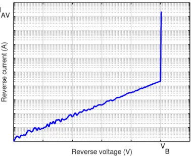
Avalanche-capable silicon devices bypass the need for flyback diodes or TVS by taking advantage of im-pact ionization. Imim-pact ionization allows reverse-biased transistors to dissipate power from a voltage spike by briefly allowing the current to increase by orders of magnitude while keeping the voltage nearly fixed. By clamping the voltage at a safe level as seen in Figure 2.2, the electric field in the switch is limited. This prevents irreversible dielectric breakdown in thin oxides or other passivation layers in a device. By selecting devices that operate within the limits of VB and the peak avalanche current (IAV), circuit designers can
make converters and other high-power circuits where transistors reliably handle unexpected power surges without flyback diodes.
Figure 2.2: Reverse-bias I-V characteristics representative of an avalanche-capable device.
Device manufacturers typically give a single pulse avalanche energy (EAS) by performing an unclamped
inductive switching (UIS) test. Figure 2.3 shows waveforms typical of avalanche operation in a UIS test. VGS is initially high and the switch is on, charging up the inductor. When VGS goes low, the switch blocks
all current. Since the voltage across the inductor is V = LdI
dt, the sudden drop in current produces a large negative voltage VDS seen at the transistor’s drain. Robust devices can go into avalanche breakdown which
clamps VDS and prevents it from increasing beyond VB damaging dielectrics in the device. Since the current
is allowed to increase by many orders of magnitude, well-designed switches will only get damaged if the energy stored in the inductor increases the temperature in the device above a critical value Tj,destr [10]. Although
reliability as it can be shown to vary with the UIS test parameters [4]. Manufacturers also typically designate safe operating areas on datasheets by quoting IAV as a function of the time spent in avalanche [35]. As circuit
designers may often not have a value for the parasitic inductance in a circuit and UIS can differ drastically from realistic situations, IAV and VBare typically used to assess a device’s suitability for a given application.
Figure 2.3: Waveforms showing the drain voltage clamping (black) when the inductor current quickly drops (blue).
Although GaN diodes have shown avalanche breakdown [14], it’s still not well understood. GaN pn diodes have shown clear signs of avalanche such as voltage clamping [23], though they have very limited peak avalanche current values [29] and have not been thoroughly characterized like commercial avalanche-capable devices. In addition to voltage clamping, one study on thin GaN pn diodes [24] also characterized the reverse-bias electroluminescence which is occurs due to band-to-band recombination caused by impact ionization.
Claims of avalanche breakdown in GaN Schottky diodes are questionable as there has either been no clear voltage clamping [42] or have extremely high pre-breakdown leakage current [31]. Signs of impact ionization however, have been demonstrated. In particular multiple studies have seen reverse-bias electroluminescence at the perimeter of the gate Schottky contacts used in GaN HEMTs [13] [21] [3]. Since GaN power devices are primarily n-type, demonstrating impact ionization as seen in similar silicon devices without p-n junctions [5] is an important step to enabling avalanche-capable GaN transistors.
2.1.2
From Impact Ionization to Avalanche Breakdown
Avalanche breakdown occurs because of impact ionization which occurs at high electric fields. Impact ion-ization is a physical process where a hot carrier impacts an atom in the lattice, ionizing it and creating an electron-hole pair. Hot carriers are electrons (holes) in the conduction (valence) band that have gained a large amount of kinetic energy by drifting through a high electric field region. As the processes involved in hot carriers gaining energy from the electric field and losing energy through collisions are highly dependent on a material’s intrinsic properties, impact ionization varies significantly between materials.
Though many theories on impact ionization in semiconductors and dielectrics have been proposed [45] [27], it can be phenomenologically described by impact ionization coefficients for each type of carrier. The co-efficients α (β) are functions of the electric field and represent the number of electron-hole pairs generated per unit distance by a hot electron (hole). Due to the process’s strong dependence on the electric field, the coefficients are typically parameterized as
α(E) = Ane−Bn/E (2.1)
β(E) = Ape−Bp/E (2.2)
The values of An, Ap, Bnand Bpfor a given material depend on the details of how carriers are allowed to
gain energy. Monte Carlo transport simulations with details of the band structure [15] are typically used to calculate the coefficients [25] however, a material’s bandgap, Eg, gives some intuition about the process. More
specifically, since the energy required to create an electron-hole pair is at least Eg, the ionizing carrier needs
to gain more energy than that from the electric field. This means that the onset of impact ionization will occur at higher electric fields for wider bandgap materials. This trend is partially responsible for the increase in Ecwith Egthough the details for certain materials and the exact dependence is still being investigated [36].
Impact ionization is necessary for avalanche breakdown but by itself not enough to sustain the increasing current during avalanche breakdown. A device-specific multiplication factor Mn (Mp) is typically defined to
describe the increase in current specifically due to impact generation initiated by electrons (holes). These multiplication factors are defined as
1 − 1 Mn = Z W 0 αe−R0x(α−β)dx 0 dx (2.3) 1 − 1 Mp = Z W 0 βe−RxW(α−β)dx 0 dx (2.4)
where W is the width of the depletion region. The right-hand side integrals represent the average number of electron-hole pairs generated per hot electron (hole) that crosses the drift region. As the integrals approach 1, each carrier that crosses the drift region produces another carrier that repeats the process. In this self-sustaining process, M → ∞ and the current rapidly increases by orders of magnitude which is avalanche breakdown.
2.1.3
Indicators of Avalanche Breakdown
Besides the rapid increase in current, another sign of avalanche is a slight negative differential resistance (NDR) during breakdown [26]. When the electric field is high enough for impact ionization in a reverse-biased pn junction, a small increase in current temporarily increases the width of the space charge region (SCR). This charge mostly comes from dopants at the edges of the SCR since the leakage through the junction is low. The increase in charge in the SCR raises the electric field by a constant amount causing more carriers to be generated through avalanche. Due to the exponential behavior of avalanche, the charge of the generated carriers is larger than the extra SCR charge and the excess carriers temporarily shorten the SCR below its original width causing the voltage to decrease. This small decrease in voltage with a small increase in current is the origin of the NDR during avalanche and similar behavior is expected in devices that undergo avalanche without pn junctions [5].
Due to the electron-hole pairs generated in the high field region, band-to-band recombination (BTBR) is also expected. BTBR produces reverse-bias electroluminescence with peak emission energy at Eg. Below
bandgap luminescence is also expected since traps play a role in carrier recombination, but the majority of the emission occurs near or above Eg. Luminescence is useful for understanding avalanche in devices since
undergo avalanche first to design devices that have more uniform avalanche. This electroluminescence can also be used to determine where electric field peaks occur which is beneficial for designing proper edge ter-mination for higher breakdown voltages.
The temperature dependence of impact ionization is one of the unambiguous signs of whether avalanche breakdown is occuring or not. Each time a hot carrier has a collision with other carriers, phonons or de-fects, it loses some energy. Since carriers only gain energy from the electric field in between collisions, their scattering rate limits impact ionization. In particular, high temperatures mean more phonons to scatter the hot carriers leading to lower impact ionization generation rates. An equivalent way to think about the temperature dependence of the impact ionization generation rate is that high temperatures lead to a shorter mean free path which gives carriers less time between collisions to gain kinetic energy from the electric field. This corresponds to an increase in VB with temperature.
2.1.4
Impact Ionization Rates in GaN, SiC and Si
When the electric field profile within a device is known and impact ionization can be selectively initiated by one type of carrier, the impact ionization coefficients can be determined by measuring the current increase. This is most easily accomplished by shining above bandgap light on reverse-biased pn photodiodes. The light generates electron-hole pairs which drift in opposite directions due to the electric field. The location of the illumination determines which type of carrier drifts through the lowly-doped drift region where the electric field is highest and where impact ionization mostly occurs. This type of measurement can also be done with Schottky diodes, though only one type of carrier generated in the semiconductor will pass through the drift region [41]. By subtracting the leakage current without illumination from the photocurrent and normalizing by the its value when M = 1, the multiplication factors and impact ionization coefficients can be determined.
Though these photodiode measurements can be routinely done, appreciable impact ionization only oc-curs at high electric fields. This requirement has limited this type of measurement in GaN to devices with thin drift regions which are more suited for avalanche photodiodes than power electronics. Furthermore, the majority of these measurements in GaN have been on heteroepitaxial layers on foreign substrates such as silicon, SiC and sapphire. These substrates are also not ideal for power electronics since they typically have dislocation densities above 107 cm-2 which can significantly increase leakage in devices. Photodiode
measurements on high dislocation density substrates also adds uncertainty to the ionization coefficients since defects can play a role in carrier generation and recombination processes.
For a clear understanding of why GaN power devices lack avalanche, it’s necessary to compare GaN photodiode measurements with silicon and SiC. Few measurements of impact ionization have been done in homoepitaxial bulk GaN photodiodes [6] [22]. Cao et. al. fabricated thin vertical GaN pn diodes and an InGaN interlayer between the substrate and drift region was used to facilitate initiating impact ionization by both types of carriers. The results were in general agreement with results of Monte Carlo simulations by Oguzman et. al. [16] [28] and the impact ionization coefficients were determined to be
α(E) = 4.48 × 10⁸e−3.39×10⁷/E (2.5)
β(E) = 7.13 × 10⁶e−1.46×10⁷/E (2.6)
and are plotted below in Fig. 2.4 (left).
Maeda et. al. on the other hand fabricated GaN pn diodes with significantly thicker drift regions and used a beveled mesa edge for electric field management. With these devices and by assuming equal impact ionization coefficients for electrons and holes in GaN, they uesd photocurrent measurements to obtain the following values:
α(E) = β(E) = 1.3 × 10⁶e−1.18×10⁷/E (2.7) Although the assumption of equal impact ionization coefficients in GaN is questionable, the results by Maeda et. al. follow the same trend as hole impact ionization coefficients in the other measurements and simulations. This is expected the magnitude of the coefficients is much higher for holes than electrons in GaN.
Figure 2.4: Parametrized impact ionization coefficients for bulk GaN, SiC and Si from photodiode measure-ments (left) and Monte Carlo calculations of bulk GaN (right) [28].
As seen in Figure 2.4, holes in GaN begin to generate a significant amount of carriers at just over 2 MV/cm while electrons don’t even reach 1 carrier generated per micron traveled until 3 MV/cm. Although this large difference in ionization coefficients can be useful in photodiodes, GaN power devices nearly always have n-type drift regions. Since the leakage current which is responsible for initiating avalanche is primarily electrons, avalanche breakdown should not be expected to occur in GaN power devices with peak electric fields below 3 MV/cm. In contrast, the ionization coefficients for silicon [34] and SiC [20], shown in Figure 2.4 (right), are much higher for lower electric fields. Many GaN power devices experience destructive break-down, either due to high leakage or dielectric breakbreak-down, before an appreciable region of the drift region reaches 3 MV/cm.
2.1.5
Designing Avalanche-Capable Power Devices
Although high electric fields are required for avalanche, designers primarily focus on minimizing electric field peaks. By smoothing out electric field peaks, premature dielectric breakdown in passivation layers can be prevented leading to higher breakdown voltages. To design practical avalanche-capable devices, designers must achieve the contrasting goals of (1) minimizing peaks in the electric field profile and (2) ensuring that the electric field profile is sufficiently high at the target VB for avalanche breakdown to occur. Since the
used as gate oxides and passivation layers (shown in Table 2.1), a well-designed device can easily meet these two goals. However, due to the much higher electric field required for impact ionization in GaN, achieving avalanche breakdown has proven to be difficult. This means GaN devices must be carefully designed so that the field in the semiconductor is high enough at breakdown while the fields in the passivation layers remain low enough to prevent dielectric breakdown.
Material Ec (MV/cm)
Al2O3 4
SiNx 3-8
SiO2 10
Table 2.1: Critical electric field and relative permittivity for common passivation materials.
2.2
Schottky Diode Design and Simulation
2.2.1
Schottky Diode Design
The peak electric field as a function of the applied reverse-bias in a 1D Schottky junction where the drift layer is thicker than the depletion region is given by
Epk(V ) =
r
2qND(φbi+ V )
ε (2.8)
where φbi is the relatively small built-in potential [9]. Once the depletion region extends across the entire
drift layer, which is known as punchthrough, any excess bias is supported by a linear voltage drop across the depletion region. After punchrough the peak electric field is given by
Epk,pt(V ) = r 2qND(φbi+ Vpt) ε + V − Vpt W (2.9)
where Vpt, the voltage at which punchthrough occurs, is given by
Vpt=
qNDW2
Figure 2.5: Equations 2.7 and 2.8 for ND=7e15 cm−3, φbi = 0.88V and various values of W . This simple
model breaks down when the electric field becomes high enough for a significant amount of impact ionization to occur. This point is marked by the dashed red line for GaN.
For electric fields near Ec, impact ionization affects the carrier concentration profile which modifies the
dynamics of the electric field and this model breaks down. However, this simple model is useful for estimat-ing the VB at which avalanche breakdown should occur for a given ND and W . To minimize the impact of
leakage current on the I-V characteristics, this work focuses on low-voltage Schottky diodes. As seen from Eq. 2.8, to get high electric fields at a given voltage, a thin drift region and high doping is required. Due to the limited availability of bulk GaN, using an entire 2-inch wafer to grow a thin, highly-doped epitaxial drift region was not possible. To overcome these limitations, devices were designed to take advantage of the electric field peaks at the anode edges. By fabricating multi-finger Schottky diodes, the electric field peaks which occur along the finger edges allow a high electric field to cover a large area without the need for high reverse biases. These devices were used to investigate the breakdown behavior of n-type GaN devices under high electric field.
2.2.2
Simulation Methodology
The multi-finger diodes were simulated using Silvaco Atlas and modeled as a periodic array of equally-spaced rectangular anodes. The device models were further simplified to have a single lowly-doped layer of GaN
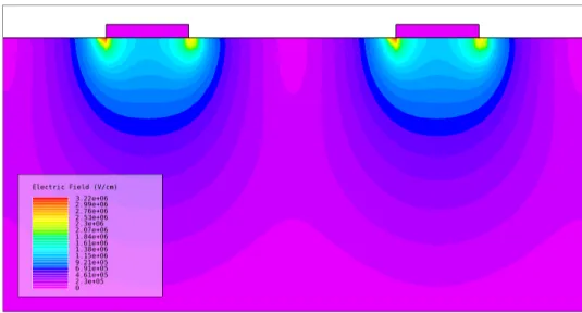
with a backside cathode. The two anodes were tied to the same bias and periodic boundary conditions were explicitly used. As seen in the upper portion of the device in Figure 2.7, the simulated electric field profile for this particular diode reaches about 3.2 MV/cm at 200 V. Although the exact values of the electric field are expected to differ in real devices due to slight variations created during fabrication, the electric field profile is qualitatively accurate.
Figure 2.6: Simplified device structure used in Atlas simulations.
Since impact ionization has an exponential dependence on the electric field, the model parameters used have a strong effect on the simulation results. The Selberherr impact ionization model from Equations 2.1 and 2.2 was used with the values of An, Ap, Bn and Bp extracted by Cao et. al. from measurements on
bulk GaN pn diodes with the InGaN interlayer [6]. With these parameters the impact ionization coefficients α(E)and β(E) are defined and then the ionization generation rate at each node in the GaN is calculated as
G = α(E)|Jn| + β(E)|Jp| (2.11)
2.2.3
Simulation Results
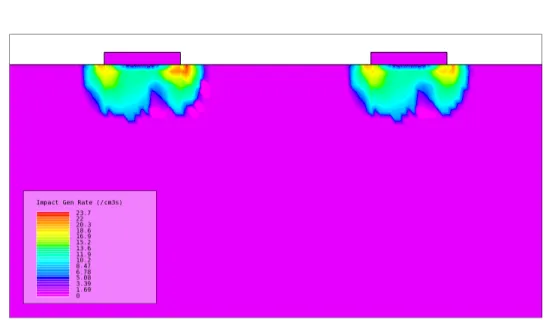
Figure 2.9: Simulated reverse bias IV characteristics for a multi-finger device.
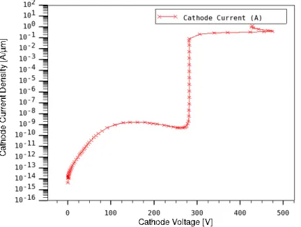
To verify that this type of device can undergo avalanche at low voltages, the impact generation rate was plotted for the same portion of the device in Figure 2.7. The generation rate near each contact is orders of magnitude higher than in the bulk of the device as expected from the electric field profile. While this verifies that impact ionization occurs at lower voltages, this alone does not necessarily mean the device undergoes avalanche. To see that avalanche truly occurs, the simulated IV curve should show an increase by orders of magnitude near the onset of impact ionization. To simulate the IV curve accurately, Silvaco’s Curvetrace algorithm was used. The Curvetrace uses a dynamic load line approach to automatically switch between voltage and current control. In this case, the cathode voltage is swept pre-breakdown since the current changes slowly. When avalanche commences, current control is used since the voltage is nearly fixed at VB. Figure 2.9 shows the expected behavior in the simulated IV curve for this device. When the
cathode current approaches 80 mA/µm, this IV curve shows pause in the voltage clamping followed by a second breakdown. This voltage clamping pause, which determines the peak current IAV, occurs due to the
large carrier concentration that accumulates during avalanche. As the current density J increases so do the carrier concentrations n and p. Also since electrons and holes generated in the drift region travel in opposite directions, n(x) 6= p(x). When the n(x) − p(x) approach ND, the carrier imbalance significantly modifies the
a decreased value in the middle of the drift region as seen in Figure 2.10. This decrease in the electric field causes impact ionization to slow down and creates the voltage clamping pause.
Figure 2.10: "U-shaped" electric field that occurs due to buildup of charge in the drift region during avalanche. The device considered here has two highly doped layers between the drift region and the cathode, but nearly identical behavior occurs for the simplified model shown in Figure 2.6.
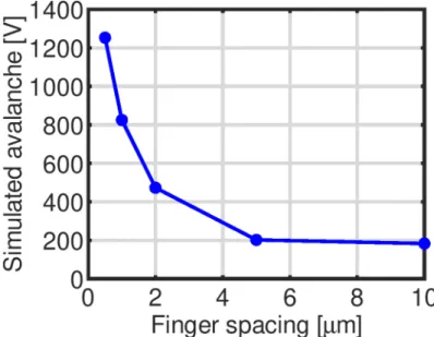
To understand how the anode design affects VB, the finger spacing and width were varied. Since the
6 µm drift layer used in simulations is typical of 650-1200 V devices, changing the anode should enable avalanche to happen at higher voltages than the VB in Figure 2.9. As seen in Figure 2.11, changing the
spacing between fingers had a drastic effect on when the simulated devices underwent avalanche. Because the fingers are held at the same potential, the initial and final potential along a horizontal line from one finger edge to the opposite edge of the other finger are the same. Then since ∇φ = −E and a shorter spacing corresponds to a smaller drop in voltage along this line, a device with smaller finger spacing will have a lower peak electric field for a given voltage. This means that the onset of avalanche breakdown will occur at much higher voltages in devices with closely packed fingers. For spacings larger than about 5 µm the sim-ulated avalanche voltage seems to saturate. In contrast, varying the finger width had small effects without discernable patterns. This is likely due to opposing electrostatic effects that occur when the width is changed.
Figure 2.11: Variation in simulated avalanche breakdown voltage with spacing between fingers.
The results in figure 2.11 show that by increasing the finger spacing, Schottky diodes with relatively thick drift regions can be capable of avalanche breakdown at low voltages.
2.3
Device Fabrication
2.3.1
Wafer Structure
While the goal of this thesis is to fabricate and characterize diodes capable of sustaining high electric fields with low leakage, relatively thick drift regions are used due to limitations on wafer availability. The original wafer, seen in Figure 2.12 on the left, has a highly-doped n+ cap layer since it was intended for vertical power FinFETs while our target device, on the right, just has a lowly-doped drift region on top of the sub-strate. The 300 µm thick c-plane (0001) oriented substrates were grown by Hitachi by hydride vapor phase epitaxy (HVPE) while the epitaxial layers were grown by IQE by metalorganic checmical vapor deposition (MOCVD) with a ND< 1016cm−3 in the drift region. Secondary ion mass spectroscopy (SIMS) detected a
high concentration of carbon used to partially compensate unintentional dopants. C-V structures were also used to determine the effective NDto be between 6-8×1015cm−3.
Figure 2.12: Original wafer structure (left) and target device structure (right).
Figure 2.13: SIMS data from original wafer (left) and C-V Schottky diode characterization.
The highly-doped cap layer was removed by electron cyclotron resonance reactive ion etching (ECR/RIE) with a Cl2/BCl3 gas. The recipe uses a Cl2/BCl3 ratio of 1:3 at an RF power between 10-35W. By using
more BCl3 than Cl2 this etch is relatively isotropic and more chemical than physical reducing the amount
of damage done to the epitaxial layer. After etching the cap layer and part of the drift region, the samples are dipped in hot tetramethylammonium hydroxide (TMAH) at 85C for 1 hour to remove the dry etching damage before continuing device fabrication.
2.3.2
Reducing Leakage Current
Figure 2.14: Defects protruding from surface after a 3 µm etch.
To minimize the amount of leakage at high reverse bias, 1-2 µm mesas are etched into the drift region. Since the depletion region starts at the anode, a deeper mesa etch means a larger reverse bias is needed for the depletion region to reach the unetched portion of the device. Figures 2.15 and 2.16 demonstrate the significance of this by showing the electric field profile at various biases for different mesa sizes. As the bias increases and the depletion region begins extending past the mesa, a peak in the electric field profile appears at the lower corner of the mesa. For the shorter mesa, this is noticeable near 300 V. Increasing the mesa height as shown in figure 2.16 reduces the electric field peak at 300 V. Though reducing this electric field peak heavily supresses the leakage current, longer etches also mean more dry etch damage which may increase the leakage as well. For etches deeper than about 2.5 µm, the dislocations and defects seen in figure 2.14 protrude out of the surface after the etch. Given these potential complications, 2 µm mesa etches were used.
Figure 2.15: Electric field profile in a Schottky diode with a 2 µm mesa and 6 µm drift region at 100 V (left), 200 V (center) and 300 V (right).
Figure 2.16: Electric field profile in a Schottky diode with a 5 µm mesa and 3 µm drift region at 100 V (left), 200 V (center) and 300 V (right).
First the surface is patternend using a standard negative resist photolithography recipe. Then a Ni hard mask is deposited and patterned by liftoff in acetone. Finally the mesas are etched in a Cl2/BCl3
plasma with 4:1 flow rate ratio at bias power of 75W and ICP power of 150W. In contrast to the n+ cap layer removal, the mesa etching is done in a Samco inductively coupled plasma (ICP-RIE) etcher as it has higher power and greater etching stability. This etch is more anisotropic and gives a more vertical sidewall profile. The higher power etch also produces sidewall damage which must be repaired to minimize the leakage.
(a) SEM image of overetched circular mesa.
(b) Square mesa under microscope. A plane in blue, M plane in red.
Figure 2.17: Various GaN test samples after etching in hot TMAH.
After the mesa etch, the sample is dipped in TMAH at 85C again to remove the sidewall damage. TMAH etches all planes of GaN except the (0001) plane. However, different planes are etched at different rates and etch rates vary between wafers meaning TMAH dips must be calibrated for each wafer. Although short overetching generally does not produce any noticeable issues, long overetches can give circular mesas jagged edges as seen in the SEM image in Figure 2.15 (a) due to the different etch rates of the (1100) and (1120) planes, or M and A planes respectively. M plane overetches are even noticeable under a microscope as shown in Figure 2.15 (b). To prevent overetching issues, hexagonal mesas were designed so the A plane was primarily exposed as seen in Figure 2.16. After sufficient etching in TMAH, the Ni hard mask and TMAH residue is removed by piranha H2SO4:H2O2 (3:1).
Figure 2.18: Hexagonal mesa with A plane exposed.
Si(OC2H5)4 or "TEOS" precursor was used for the SiO2 deposition by plasma enhanced chemical vapor
deposition (PECVD). TEOS was chosen for its ability to conformally coat the mesa sidewalls. Openings to contact the anode were etched in an ECR/RIE using a standard mixture of CF4 and H2 with a photoresist
mask.
2.3.3
Contact Deposition
The mesa etching was followed by the anode and cathode depositions. The anode, which was patterened by lift-off, used masks similar to the one in Figure 2.17. To maximize the area where impact ionization would occur, the fingers had rounded corners and were 2 µm wide, which was the minimum size that could reliably be fabricated using the standard photolithography tools in MTL. The spacing between fingers was varied between 2 and 10 µm. Control diodes were also fabricated on the same samples by using a circular pattern for the anode. After patterning the photoresist, a brief O2 plasma descumming and an HCl:H2O
(1:3) dip were done immediately before depositing the anode metal. The Pt/Au (40 nm/200 nm) anode was deposited by ebeam evaporation. Platinum was used due to its higher Schottky barrier than nickel on GaN. Then the SiO2 passivation was deposited, patterned and etched. Finally, a Ti/Al (20 nm/500 nm) cathode
was sputtered onto the backside of the sample.
Figure 2.19: Mask used to pattern the multi-finger Schottky diode anodes.
More specifically, anodes with multiple fingers, similar to that in Figure 3.9, were designed and fabricated. To maximize the area where impact ionization would occur, the fingers were 2 µm, which is the minimum size that could be reliably fabricated using the standard MTL photolithography tools, and the edges were rounded. The spacing between fingers was varied between 2 and 10 µm. The surface was patterened with
negative photoresist and a brief O2 plasma descumming and HCl:H2O (1:3) dip done before depositing the
anode metal. The anode was Pt/Au (40 nm/200 nm) deposited by electron-bean deposition. Platinum was used due to its higher Schottky barrier than Nickel on GaN. Only the SiO2passivation covering the probing
pad was etched away. The metal was then patterned by liftoff in acetone and a Ti/Al (20 nm/500 nm) cathode was sputtered onto the backside of the sample.
2.4
Electrical and Optical Characterization
2.4.1
Measured I-V Characteristics
Figure 2.20: Measured reverse bias characteristics showing sharp current increases in different multi-finger devices.
The majority of the fabricated multi-finger devices showed the sharp increase in current due to impact ion-ization though the breakdown behavior differed from the Atlas simulations. The sharp current increases, displayed in Figure 2.18, occurred at lower voltages than expected and only some of the curves showed a slight negative differential resistance.
Figure 2.21: Cross section and electric field profiles representative of the standard control diodes (left) and the multi-finger diodes (right). Compared to the control diodes, multi-finger diodes have many more points where the electric field exceeds 3 MV/cm and appreaciable levels of impact ionization can be seen in GaN.
Since the only difference between the fabrication process of the multi-finger diodes and control diodes with circular anodes was the shape of the anode, trap filling can be ruled out as the cause of the sharp current increase. By observing luminescence emitted during the reverse bias sweep, the location of the peak electric field can be determined. All multi-finger devices that showed the sharp current increase began by showing electroluminescence only at the tips of the fingers. This could explain the discrepancy with simula-tions as the rounded tips of the fingers aren’t taken into account by the two-dimensional simulation. This could also explain why some multi-finger diodes didn’t show the sharp current rise as seen in Figure 2.19. Though the multi-finger diodes were nominally identical, the avalanche occurs over such a small area that slight variations in the anode metal or wafer quality at these points could easily supress it. Furthermore, the devices showed the same voltage clamping pause seen in simulations. Since this behavior occurs due to a high avalanche current density, devices designed such that avalanche occurs over a larger area are expected to show even higher peak current values.
Figure 2.22: Measured reverse bias characteristics for circular control diode and a multi-finger diode without the sharp current increase.
2.4.2
Reverse Bias Electroluminescence
Though luminescence was initially only observed at the finger tips, luminescence could be seen along the fingers by holding the voltage for longer intervals. More specifically, the voltage was swept from 0 V past the previously mentioned sharp current increase then held constant. Figure 2.20 (b) shows 3 different devices with reverse-bias electroluminescence along the finger edges. Devices that were limited to a lower current compliance (around 4 mA), were functional after multiple sweeps showing luminescence.
(a) Microscope image of a multi-finger device for reference.
(b) Electroluminescence seen in different multi-finger diodes.
2.5
Conclusion
This chapter investigated breakdown in n-type GaN Schottky diodes. By carefully designing the anode, high electric fields were generated in GaN over a large area. These high electric fields enabled impact ionization
which led to reverse-bias electroluminescence. In addition to the luminescence, the devices also showed sharp increases in current characteristic of avalanche breakdown. Although the temperature dependence of VBwas
not determined, this work represents an important step towards understanding avalanche breakdown in GaN and enabling avalanche-capable GaN transistors.
Chapter 3
Fabrication of Vertical GaN Power FinFETs
3.1
Vertical Power Transistors
3.1.1
Introduction
The majority of discrete high-power transistors utilize a vertical structure allowing them to reliably support high current densities and high breakdown voltages. In these structures, the current rating is proportional to the area of the device while the breakdown voltage is determined by the thickness of the drift region. This makes the process of scaling devices for higher current/voltage ratings significantly simpler than in lateral devices. Additionally, current scaling with area leads makes it easier to achieve smaller chip sizes. In switching power converters, smaller devices are preferred due to their low capacitance. By utilizing devices with low capacitance, converters can operate at high frequencies while maintaining high efficiencies. Vertical transistors also typically show improved reliability over their lateral counterparts. By having electric field peaks occur within the device rather than on the surface as in lateral devices, the electric field becomes easier to manage and passivation layers are become less susceptible to dielectric breakdown. Although ver-tical devices are more difficult to integrate than lateral devices, in situations where discrete components are acceptable and efficiency and reliability are a priority, vertical structures are ideal.
Despite the numerous advantages of vertical structures for high-power devices, the vast majority of commercial GaN power devices are based on a lateral HEMT structure. GaN HEMTs are able to achieve ex-ceptionally high mobilities of 2000 cm2/Vs with high carrier density due to the 2DEG at the III-nitride/GaN
interface. Advanced electric field management and leakage current reduction mechanisms have enabled de-vices with VB in the kilovolt range [18] and the commercialization of devices rated for 650 V. In spite of these
achievements, current scaling is a fundamental issues in GaN HEMTs. Since the current is proportional to the length of the device, large chip sizes are required for high current ratings. The large size increases para-sitic capacitances and switching losses, limiting the range of frequencies for power converters. Furthermore, breakdown voltages are typically lower than expected from GaN’s theoretical Ec. Many of the causes of this
premature breakdown stem from the HEMTs lateral structure. In these devices the highest electric field peak typically occurs near the surface at the drain-side of the gate or the gate’s field plate. This high electric
field near the surface poses a potential issue for the relatively thin dielectric layers used for passivation and typically leads to premature breakdown in GaN HEMTs. Due to the shortcomings of lateral GaN power devices, next-generation devices for higher ratings will require a vertical structure.
3.1.2
Vertical GaN Transistor Structures
Vertical GaN power transistors have been under development since at least 2008 [7] and multiple device architectures have been demonstrated. Currently, the three most competitive structures for vertical GaN transistors are power FinFETs, CAVETs and MOSFETs. Power FinFETs and CAVETs overcome the short-comings of p-type GaN while MOSFETs are more similar to their silicon and SiC counterparts. Fully vertical devices on bulk GaN substrates have been demonstrated for all three structures and much work has been done to create fully and quasi-vertical transistors on GaN on non-native or engineered substrates.
The vertical GaN MOSFET is the most common of the three structures. It typically consists of a highly doped n+ GaN substrate with a thick, lowly doped n- GaN drift region a thin p-type GaN channel and an n+ cap layer for the top ohmic contact. This epilayer structure does not require selective-area regrowth which removes the need to implant Mg for the p-type doping. By creating the p-type GaN during growth, less damage is introduced and a larger fraction of the Mg dopants can be electrically activated. However, p-type GaN has low mobility which makes the channel a bottleneck for the current density.
n+ GaN n+ GaN p- GaN p- GaN n- GaN n+ GaN substrate Drain Gate Gate oxide Source Source
CAVETs bypass the issues in GaN MOSFETs by using electrons as the majority carriers throughout the device. This is accomplished by using an n-type channel. To allow switching, CAVETs have a buried p-type layer which acts as an aperture for the current. In the off-state this layer blocks the flow of current enabling high breakdown voltages. Although CAVETs are a significant improvement over vertical GaN MOSFETs, their fabrication is a fairly complex process. In particular, creating the buried p-type layer by either ion implantation or selective-area regrowth currently presents a significant challenge.
n+ GaN n+ GaN p- GaN p- GaN n- GaN n+ GaN substrate Drain Gate Gate oxide Source Source
Figure 3.2: Vertical CAVET structure on bulk GaN.
Power FinFETs remove the need for this buried p-type layer by using sidewall depletion to switch the flow of electrons. These devices typically consist of a highly doped n+ GaN substrate with a thick lowly doped n- GaN drift region and a thin n+ GaN cap layer. Power FinFETs have arrays of long fins with sub-micron widths. By using a sufficiently high workfunction gate metal around the sides of the fin, the depletion region extends across the entire fin at VGS = 0, enabling a normally-off transistor. The sub-micron fins also help
reduce leakage current in the off-state enabling high VB. Although the first generation of these devices were
capable of up to 1.2 kV and 5 A in an area below 0.5 mm2, the fabrication technologies used were not easily
scalable. This chapter explores alternative fabrication technologies for scaling vertical power FinFETs to larger sizes for higher current ratings. In particular, more robust processes are developed for defining and etching the fins, setting the gate height and etching the gate oxide.
n+ GaN n+ GaN Field oxide n- GaN n+ GaN substrate Drain Spacer Gate Gate oxide Source
(a) Vertical Power FinFET structure on bulk GaN.
(b) SIMS results from bulk GaN wafers used for vertical power FinFETs.
Figure 3.3: Vertical Power FinFET device and wafer structure.
3.2
Fabrication Technologies
3.2.1
Main Fabrication Steps
The main fabrication steps for vertical power FinFETs are shown in Figure 3.4. Fabricating vertical power finFETs begins by using electron-beam (ebeam) lithography to pattern metal sub-micron fins in the device active region (a). The exposed GaN is then etched to define the 1 µm tall fins (b). After removing the metal mask (c), the field oxide is conformally deposited and etched down to the appropriate height (d). A similar conformal deposition and etching process is repeated for the gate stack (e). After the gate stack is deposited an oxide spacer layer is deposited and etched back (f) to separate the gate metal from the source. An ohmic recess is then done to minimize the source contact resistance then the contact is deposited and patterned (g). The final step is the deposition of the drain on the backside of the sample (h).
n+ GaN n- GaN n+ GaN substrate (a) n+ GaN n- GaN n+ GaN substrate (b) n+ GaN n- GaN n+ GaN substrate (c) n+ GaN n- GaN n+ GaN substrate Field oxide (d) n+ GaN n- GaN n+ GaN substrate Field oxide Gate oxideGate
(e) n+ GaN n- GaN n+ GaN substrate Field oxide Spacer Gate oxideGate
(f) n+ GaN n- GaN n+ GaN substrate Source Field oxide Spacer Gate oxideGate
(g)
n+ GaN
n- GaN n+ GaN substrateDrain
Source
Field oxide Spacer Gate oxideGate
(h)
Figure 3.4: Main fabrication steps for vertical power FinFETs.
3.2.2
Fin Patterning Process
The standard lift-off process to pattern the metal mask that is used to define and etch the fins (shown in Figure 3.4) is difficult to scale. Due to the high density of sub-micron fins in the mask, lift-off is slow and typically starts from the edge of each device. This works well enough for devices under 1 mm2, but lift-off
mask frequently has subpar adhesion. Since the width of the depletion region in the fins determines the turn-on voltage, significantly wider fins are not a feasible option for normally-off transistors.
Photoresist
(a) (b)
(c) (d)
(e) (f)
Figure 3.5: Standard lift-off process for patterning hard mask to etch fins. (a) PMMA is spincoated onto the wafer. (b) Ebeam lithography is used to pattern the PMMA. (c) A Ni hard mask is evaporated onto the wafer. (d) The remaining PMMA is washed away with hot NMP removing the excess Ni. (e) The GaN is dry etched with the Ni mask used to define the fins. (f) The Ni mask is removed with piranha.
A more suitable method of patterning closely packed sub-micron fins over a large area is a metal-first process. As seen in Figure 3.5, the metal mask is deposited first followed by standard lithography steps to define the pattern. The exposed metal is then etched and the remaining photoresist is rinsed away. This overcomes the adhesion problems in the lift-off process. As an added benefit, in this process photoresist never comes into direct contact with the GaN which minimizes a potential source of residue on the surface.
This work investigates two metal-first processes as alternatives to lift-off for patterning the fins.
Photoresist Metal Hard Mask
(a) (b)
(c) (d)
(e) (f)
Figure 3.6: Metal-first process for patterning hard mask to etch fins. (a) A metal hard mask is deposited onto the wafer followed by spincoating with photoresist. (b) Ebeam lithography is used to pattern the photoresist. (c) The metal hard mask is etched with photoresist used to pattern the metal. (d) The remaining photoresist is removed in acetone or NMP. (e) The GaN is dry etched with the metal hard mask used to define the fins. (f) The metal hard mask is removed by wet etching.
The main challenge in a metal-first process is ensuring that each etch is chemically compatible with the various layers. This means that each etch step should be selective enough between the mask and the underly-ing layer. Since the GaN fins are etched in a high-power BCl3/Cl2 inductively coupled plasma (ICP), nickel
(Ni) is preferred as a hard mask because of its chemical inertness to this plasma. Although this increases the selectivity of the GaN etching step, it also makes Ni difficult to pattern by dry etching. Due to the lack of
![Table 1.1: Critical electric field, bandgap relative permittivity, electron mobility and Baliga figure of merit (normalized to Si) for relevant materials [36] [30].](https://thumb-eu.123doks.com/thumbv2/123doknet/14744753.577800/18.918.184.736.451.600/critical-electric-relative-permittivity-electron-mobility-normalized-materials.webp)
![Figure 2.4: Parametrized impact ionization coefficients for bulk GaN, SiC and Si from photodiode measure- measure-ments (left) and Monte Carlo calculations of bulk GaN (right) [28].](https://thumb-eu.123doks.com/thumbv2/123doknet/14744753.577800/30.918.112.799.112.406/figure-parametrized-ionization-coefficients-photodiode-measure-measure-calculations.webp)