The Effect of Nucleation on the Quality of MBE-ZnSe/III-V Heterostructures
by
Emily L. Warlick
Submitted to the Department of Electrical Engineering and Computer Science in Partial Fulfillment of the Requirements for the Degrees of Bachelor of Science in
Electrical Engineering and Computer Science
and Master of Engineering in Electrical Engineering and Computer Science at the Massachusetts Institute of Technology
December 16, 1996
-7~7
Copyright 1996 Emily L. Warlick. All rights reserved.
The author hereby grants to M.I.T. permission to reproduce and distribute publicly paper and electronic copies of this thesis
and to grant others the right to do so.
Author
Department of Electrical Engineering and Computer Science December 16, 1996 Certified by Leslie A. Kolodziejski Thesis Supervisor
/1 4
/ ~ Accepted byOCT 291997
1 • . F. R. MorgenthalerChairma DW-eartment Committee on Graduate Theses
n1:-KJ11
\The Effect of Nucleation on the Quality of MBE-ZnSe/III-V Heterostructures
by
Emily L. Warlick Submitted to the
Department Of Electrical Engineering and Computer Science December 16, 1996
In Partial Fulfillment of the Requirements for the Degree of Bachelor of Science in Computer Science and Electrical Engineering and Master of Engineering in Electrical Engineering an Computer Science
ABSTRACT
ZnSe-based II-VI semiconductors represent an area of intense research, due to their promise as blue emitters for high-density optical storage systems and a range of other applications. The state-of-the-art ZnSe-based injection laser diodes that have been demonstrated to date are primarily pseudomorphic structures grown on GaAs substrates with GaAs epitaxial buffer layers. Recent electrical degradation studies have led to a growing consensus that defects arising from the ZnSe/GaAs interface presently play the limiting role in the lifetime performance of these devices. Various reports have also suggested that different nucleation procedures can lead to significant changes in the structural properties of the ZnSe overlayer. In this study, we have examined the effects of the GaAs surface reconstruction and the use of Zn or Se pre-exposure on the resultant defect densities observed in 1 p.m ZnSe films grown by molecular beam epitaxy.
In order to examine the role of lattice-mismatch on the ZnSe defect density, we have also studied ZnSe grown on lattice-matched novel buffer layers of (In,Ga,A1)P on GaAs substrates. It is possible to grade the lattice constant of the buffer layer from that of GaAs to that of ZnSe. The study of these buffer layers is further motivated by their use as a p-type ohmic contact to a p-p-type ZnSe overlayer. We have also studied defect generation in ZnSe epilayers grown on relaxed graded buffer layers of (In,Ga)P with the phosphide surface capped with 8 monolayers of GaAs. In this manner, surface chemistry is removed as a variable while achieving a buffer layer that is lattice-matched to ZnSe. These studies have indicated that growth of ZnSe on (2x4)-reconstructed GaAs results in a defect density significantly lower than for growth of ZnSe on c(4x4)-reconstructed GaAs.
Thesis Supervisor: Leslie Kolodziejski
Acknowledgements
I could not have completed this research in its present state without the support of a handful of people:
* Professor Leslie Kolodziejski, for providing me with the opportunity to study this exciting area of semiconductor development, and for her unending guidance,
encouragement, and support.
* Dr. Gale Petrich for helping me to learn how to run both the III-V and the II-VI systems, for always being willing to sit in the lab when I went to class, and for teaching me the difference between the east and west coast swings.
* Dr. Easen Ho for so patiently teaching me how to run the II-VI MBE chamber and for helping to get my research off to a terrific start.
* Jody House for the TEM analysis of a large number of my samples.
* Professor Fitzgerald for helpful discussions relating to semiconductor defects. * Angela Odoardi-Mickunus for satisfying my need to talk about veggies on a regular basis and for her kindness and compassion.
* Amy Duwel for the coffee breaks, the jogging, and for her support through the endless ups and downs of life in and out of the lab.
* Jeremy Milikow for taking breaks with me, particularly during the writing of this thesis.
Most of all, I would like to thank my family for supporting and encouraging my academic pursuits over the past two decades and for their full and unqualified love.
Table of Contents
1. Introduction 15
1.1 Background ... 15
1.2 H istory ofZnSe ... 16
1.3 Alternative Materials Systems--GaN ... 19
1.4 Outline of Thesis ... ... 21
2. Molecular Beam Epitaxy of ZnSe 23 2.1 Crystal Structure of ZnSe ... ... 23
2.2 Theory of Molecular Beam Epitaxy ... 23
2.3 Epitaxial System and Experimental Setup ... 25
Growth Preparation ... ... ... 25
III-V GSMBE Growth ... ... 26
II-VI M BE Growth ... ... 26
2.4 N-Type Doping Using ZnCl2 ... . ... .. . . 29
2.5 P-Type Doping Using an RF Nitrogen Plasma Source ... 30
3. Materials Challenge 33 3.1 Lattice Match ... 33
3.2 (In,Ga,A1)P: Pre-Growth Calculations and Analysis ... 34
Lattice Constant: Calculations ... ... 34
Lattice Constant: Analysis ... 38
Energy G ap ... ... 40
3.3 N ucleation ... 41
4. Growth and Characterization 45 4.1 ZnSe/(In,Ga,Al)P/GaAs: Effect of Bandgap Match ... 45
4.2 ZnSe/GaAs: Effect of Nucleation ... ... 51
G aA s ... ... 51
ZnSe ... ... ... 54
ZnSe/GaAs ... ... ... 55
MBE-ZnSe/c(4x4)-reconstructed GaAs ... 56
MBE-ZnSe/(2x4)-reconstructed GaAs ... 59
Migration Enhanced Epitaxy ... ... 62
4.3 ZnSe/GaAs/(In,Ga)P: Effect of Lattice Mismatch ... 63
5. Future Research
5.1 LED Structure: Design and Analysis ... 77
5.2 Recent Advance ... 78
5.3 Future Pursuits ... 79
Appendix A: In-Situ Characterization Techniques 81 A. 1 Reflection High Energy Electron Diffraction ... 81
A.2 Auger Electron Spectroscopy ... ... 82
Appendix B: Structural Characterization 83 B.1 X-Ray Double Crystal Diffraction ... 83
B.2 Photoluminescence ... ... 84
B.3 Cathodoluminescence ... ... 84
B.4 Atomic Force Microscopy ... ... 85
B.5 Transmission Electron Microscopy ... 85
B.6 Etch Pitting ... 86
Appendix C: Electrical Characterization 89 C. 1 ZnSe pn-junction Diodes ... ... 89
C.2 ZnSe Light-Emitting Diodes ... .... 89
C.3 I-V Measurements ... ... 90
List of Figures
Figure 11: Bandgap versus lattice constant for II-VI and m-V binary materials. The ellipse in the middle indicates the spectral sensitivity of the human eye. The edge of red light detection is at 1.8 eV; the edge of blue light is at 3.1 eV.
Figure 1.2: Timeline of progress of II-VI based light emitting diodes.
Figure 2.1: Schematic diagram of the MIT heteroepitaxial system: IlI-V GSMBE chamber, II-VI MBE chamber, and a UHV transfer chamber for II-VI/III-V growth.
Figure 2.2: [Cl] versus ZnCl2 effusion cell temperature, as determined by SIMS analysis.
Figure 2.3: Incorporated nitrogen concentration, [N], as a function of RF Power * Gas Pressure (reproduced from ref. 22).
Figure 3.1: An epilayer grown on a lattice-matched substrate. The in-plane lattice
constants of the two materials are equal.
Figure 3.2: A relaxed epilayer on a lattice-mismatched epilayer. The in-plane lattice
constant of the epilayer is larger than that of the substrate.
Figure 3.3: A pseudomorphic epilayer on a lattice-mismatched epilayer. The in-plane
lattice constant of the epilayer is larger than that of the substrate, so, for thin layers, the lattice is strained to match the substrate.
Figure 3.4: Lattice constant as a function of composition (reproduced from ref. 11). Figure 3.5a: RHEED oscillations during growth of GaAs. T-1Ga = 0.596 tm/hr.
Figure 3.5b: RHEED oscillations during growth of InGaP. T-' nC, = -m/hr1.113
Figure 3.6a: X-Ray double crystal rocking curve of 1 gm ZnSe grown on a GaAs buffer
layer. ZnSe peak at -2750 sec, GaAs peak at -2400 sec. FWHMGaAs = 37 sec.
Figure 3.6b: X-Ray double crystal rocking curve of lJm ZnSe grown on a graded InGaP buffer layer. ZnSe peak at -4000 sec, GaAs peak at -3200 sec. FWHMGaAs = 90 sec.
Figure 3.7: Energy bandgap (eV) versus lattice constant (a) for the (In,Ga,Al)P III-V material group and for GaAs and ZnSe.
Figure 3.8a: Schematic of a pair of stacking faults surrounded by Shockley dislocations
Figure 3.8b: Schematic of the plan view TEM image of a pair of stacking faults surrounded by Shockley dislocations nucleated at the GaAs/ZnSe interface.
Figure 3.9: Schematic of plan view TEM image of misfit dislocations in a ZnSe/GaAs structure.
Figure 3.10: Threading dislocation formed along a slip plane (dashed line).
Figure 4.1: Theoretical valence band offsets for the GaAs/ZnSe structure and the GaAs/(In,Ga,Al)P/ZnSe structure. GaAs/ZnSe has a 0.96 eV valence band discontinuity; InAlP/ZnSe has a 0.35 eV valence band discontinuity.
Figure 4.2: Photoluminescence scans of l gm ZnSe grown on InAIP. The top figure shows the scan for pseudomorphic ZnSe (not relaxed). The bottom figure shows the scan for relaxed ZnSe with a deep level centered around 2.3 eV.
Figure 4.3a: CL of Sample #2-- 1pm ZnSe on 4pm relaxed graded layer of (In,Ga)P. T = 300K; Mag = 1700x.
Figure 4.3b: CL of Sample #3-- 1pm ZnSe on 4pm relaxed stepped layer of (In,Al)P. T = 300K; Mag = 1700x.
Figure 4.3c: CL of Sample #5--1pm ZnSe on 4apm relaxed graded layer of (In,Ga,Al)P. T = 300K; Mag = 1700x.
Figure 4.4: Atomic force micrograph of 1pm ZnSe film grown by MBE on 4pm linearly graded (In,Ga,Al)P buffer layer. The mean roughness value over a 500 nm x 500 nm area was 4A.
Figure 4.5a: RHEED pattern of (2x4)-reconstructed GaAs at growth temperature (Tc=6400C).
Figure 4.5b: RHEED pattern of (2x4)-reconstructed GaAs before transfer (Tc=2700C).
Figure 4.6a: Top view and side view of c(4x4)-reconstructed GaAs (100% arsine surface coverage). (reproduced from ref. 38)
Figure 4.6b: Top view and side view of (2x4)-reconstructed GaAs (75% arsine surface coverage). (reproduced from ref. 38)
Figure 4.7: Surface configurations for ZnSe on GaAs. The trend in band offsets is based on theoretical analysis.
Figure 4.8: (a) MBE-ZnSe/c(4x4)-reconstructed GaAs with Zn and Se shutters opened
simultaneously; (b) MBE-ZnSe/c(4x4)-reconstructed GaAs with a 2 minute Zn pre-exposure; (c) MBE-ZnSe/c(4x4)-reconstructed GaAs with 1 min Se pre-exposure.
Figure 4.9: Atomic force micrograph of 1 jtm ZnSe film grown by MBE on a Zn
pre-exposed c(4x4)-reconstructed GaAs buffer layer (sample 7).
Figure 4.10: Room temperature CL image of MBE-ZnSe/(2x4)-reconstructed GaAs with
a 2 min Zn pre-exposure (sample 9); Mag=1700x.
Figure 4.11: Atomic force micrograph of 1 jpm ZnSe film grown by MBE on a Zn
pre-exposed (2x4)-reconstructed GaAs buffer layer (sample 9).
Figure 4.12a: 1 jtm ZnSe grown on c(4x4)-reconstructed GaAs with a one minute Zn
pre-exposure followed by ten cycles of MEE (cycle = 3 sec Se, 2 sec delay, 3 sec Zn) at 2600C and 24 more cycles of MEE while ramping to the growth temperature.
Figure 4.12b: 1 ptm ZnSe grown on (2x4)-reconstructed GaAs with a one minute Zn
pre-exposure followed by ten cycles of MEE (cycle = 3 sec Se, 2 sec delay, 3 sec Zn) at 2600C and 24 more cycles of MEE while ramping to the growth temperature.
Figure 4.13: Schematic of growths used to study the effect of lattice-mismatch.
Figure 4.14a: TEM micrograph of sample 9 (ljim ZnSe on (2x4)-reconstructed GaAs).
Micrograph is about 4ptm wide. TEM courtesy of Jody House.
Figure 4.14b: TEM micrograph of sample 11 ( Lm ZnSe on (2x4)-reconstructed GaAs
on a graded (In,Ga)P buffer layer). Micrograph is about 2.5Pjm wide. TEM courtesy of Jody House.
Figure 4.15a: Room temperature CL of 1 jim ZnSe film grown by MBE on 4jtm linearly
graded (In,Ga)P buffer layer with a two minute Zn-exposed eight monolayer c(4x4)-reconstructed GaAs layer between the (In,Ga)P and ZnSe (sample 10). Mag = 1700x.
Figure 4.15b: EPD photograph of 1ljm ZnSe film grown by MBE on 4jm linearly
graded (In,Ga)P buffer layer with a two minute Zn-exposed eight monolayer c(4x4)-reconstructed GaAs layer between the (In,Ga)P and ZnSe (sample 10). Mag=400x. EPD=3x10 7 cm-2
Figure 4.16a: Room temperature CL of 1 jim ZnSe film grown by MBE on 4tm linearly
graded (In,Ga)P buffer layer with a two minute Zn-exposed eight monolayer (2x4)-reconstructed GaAs layer between the (In,Ga)P and ZnSe (sample 11). Mag=1700x.
Figure 4.16b: EPD photograph of 1lm ZnSe film grown by MBE on 4gm linearly graded (In,Ga)P buffer layer with a two minute Zn-exposed eight monolayer (2x4)-reconstructed GaAs layer between the (In,Ga)P and ZnSe (sample 11). Mag=400x. EPD=1.6x106 cm-2.
Figure 4.17a: Atomic force micrograph of 1gm ZnSe film grown by MBE on 4gm linearly graded (In,Ga)P buffer layer with a Zn-exposed 8 monolayer c(4x4)-reconstructed GaAs layer between the (In,Ga)P and the ZnSe (sample 10). Ra = 7A.
Figure 4.17b: Atomic force micrograph of 1•m ZnSe film grown by MBE on 4gm linearly graded (In,Ga)P buffer layer with a Zn-exposed 8 monolayer (2x4)-reconstructed GaAs layer between the (In,Ga)P and the ZnSe (sample 11). Ra = 3A.
Figure 4.18a: 10OK photoluminescence scan of 1I m ZnSe grown with a Zn pre-exposure on c(4x4)-reconstructed GaAs (sample 7).
Figure 4.18b: 10K photoluminescence scan of 1~gm ZnSe grown with a Zn pre-exposure on (2x4)-reconstructed GaAs (sample 9).
Figure 4.19a: 10OK photoluminescence scan of 1gm ZnSe grown with a Zn pre-exposure on a graded (In,Ga)P buffer layer with a c(4x4)-reconstructed GaAs cap (sample 10). Figure 4.19b: 10K photoluminescence scan of Iglm ZnSe grown with a Zn pre-exposure on a graded (In,Ga)P buffer layer with a (2x4)-reconstructed GaAs cap (sample 11). Figure 5. 1: Schematic of pn diode showing doping and composition of each layer.
Figure 5.2: Current versus applied voltage characteristic of a ZnSe p-n diode consisting of ZnSe grown on c(4x4)-reconstructed GaAs.
Figure A. 1: ZnSe surface reconstructions for the Se-rich and Zn-rich cases. Figure A.2: Schematic of the theory of auger electron emission.
Figure B. 1: Primary features seen in PL spectra of ZnSe epilayers.
Figure B.2: Image of etch pits in sample of 1lm ZnSe/GaAs. One second etch with 1% bromine solution of bromine-methanol-250nm. EPD = 9x107 cm2.
Figure C. 1: Injection of electrons and holes under forward bias with ND>NA. Figure C.2: Theoretical ZnSe LED with ND>>NA.
List of Tables
Table 4.1: (In,Ga,Al)P layers used as buffers for 1lgm ZnSe epilayers. Table 4.2: Pre-exposures used in MBE-ZnSe/c(4x4)-reconstructed growths.
Table 4.3: Correlation between Yo and deep level transitions measured by 10K PL, and
dislocation density, DD (cm-2), measured by CL and EPD, of samples 7 and 9.
Table 4.4: Correlation between Yo and deep level transitions measured by 10K PL, and
dislocation density, DD (cm-2), measured by CL and EPD, of samples 10 and 11.
Table C. 1: Details of evaporation and thermal annealing for contacts to n-type and p-type
Chapter 1: Introduction
1.1 Introduction
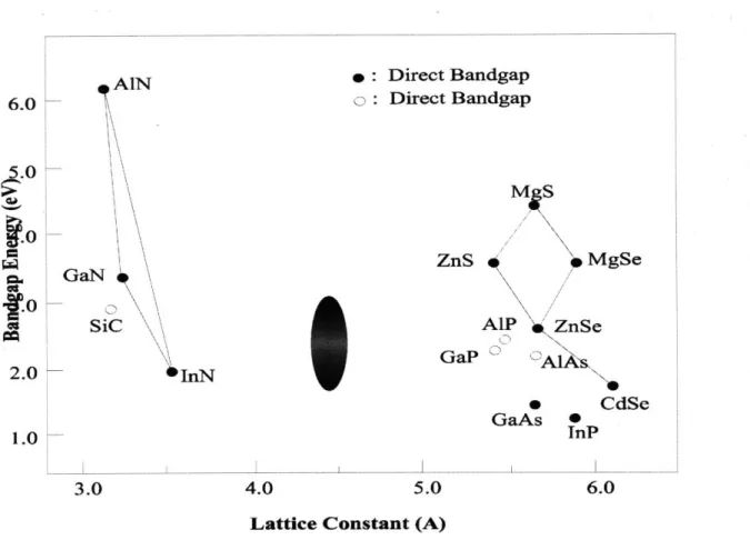
Over the past ten years, intense research has resulted in fantastic breakthroughs in the area of II-VI compound semiconductor blue/green light emitters. The large bandgap of the II-VI semiconductors allows for the possibility of developing blue light emitting devices. The wide direct room temperature bandgap of ZnSe (2.67 eV) makes ZnSe-based devices ideal for use in short wavelength light emitters. With a wavelength approximately one-half of the wavelength of the present lasers that are used in compact-disc players, ZnSe-based laser diodes will at least quadruple data density. ZnSe light-emitting diodes will also provide the missing blue color necessary for full three color displays, which are presently satisfied to a limited extent by GaN blue light emitting diodes.
Figure 1.1 shows the II-V and II-VI material systems. The large number of materials available for incorporation into ZnSe growth, most notably the group II materials Be, Mg, and Cd, and the group VI materials S and Te, allow for the growth of a highly confining active region in ZnSe-based light emitters. Such a region can significantly improve the external quantum efficiency of the diode and can yield a narrow emission spectra, resulting in sharper color output.
AIN * : Direct Bandgap 6.0 o: Direct Bandgap ,' M \S
ZnS
MgSe
GaN
SiC 2.0 OInN AlP ZnSe GaP 0 oAI1 * CdSe GaAs * 1.0 InP 3.0 4.0 5.0 6.0Lattice Constant (A)
Figure 1.1: Bandgap versus lattice constant diagram for II-VI and III-V binary materials. The ellipse in the middle indicates the spectral sensitivity of the human eye. The edge of red light detection is at 1.8 eV; the edge of blue light is at 3.1 eV.
1.2 History of ZnSe
ZnSe-based laser diodes have a long, interesting history. Research of semiconductor materials began about thirty years ago. Numerous difficulties in II-VI semiconductors, however, caused IV semiconductor research to surge ahead of the II-VI research in the late 1970s, when the research of II-II-VI semiconductors was largely relegated to academia.
In the early 1980s, research was aimed at determining the ideal growth technique for epitaxial II-VI films. Several techniques were pursued, most notably molecular beam
. By 1985, it was layers [1].
minimizing defect ality of the MBE-itial n- and p-type be much easier to maximum carrier oup at Matsushita ng source [2]. At :entration reached
Several years of research elapsed before a p-type doping source was discovered. Early p-type doping utilized Li, but the high diffusivity of Li resulted in a maximum carrier concentration of only lxl0'7 cm73. Nitrogen-doping was also studied as a candidate because it is a shallow level acceptor and has a high solubility limit in ZnSe. In 1990, Park et al. discovered a novel means of N doping whereby active nitrogen was produced by a plasma discharge [3]. By these means, p-type doping of ZnSe of up to
1x10'8 cm3 became immediately possible.
Thus, by 1991, the materials necessary to grow a ZnSe p-n junction diode was available. A few months later, a group at 3M Company announced the fabrication of the first II-VI laser diode [5]. The device emitted coherent light at a wavelength of 490 nm from a ZnSe-based structure under pulsed current injection at 77 K. Shortly thereafter, similar results were announced by a group of Brown/Purdue University researchers [6].
After this breakthrough, new problems arose, causing long delays before room temperature continuous wave (CW) operation was announced by the Sony Corporation in 1994 [7]. This delay was primarily due to the difficulty of obtaining an ohmic contact to p-type ZnSe. Initial contacts utilized Au, but they exhibited high contact resistance. The first room temperature CW operation of a II-VI laser diode used Pd/Pt/Au ohmic metals to reduce the operating voltage of the device. Au is required as a contact to external devices and the Pt acts as a barrier between the Pd and Au layers to keep the Au from diffusing into the device.
The present thrust of the II-VI saga is to increase the lifetime of the laser diodes, primarily by decreasing the defect densities in the active region of the devices. The first room temperature (RT) diode from Sony Corp. operated for 9 seconds [7]. In February
1996, this same group announced a lifetime of 100 hours under room temperature CW operation with a constant light output power of 1mW [8]. The defect density of this laser diode was reported to be 3x103 cm-3.
1.3 Alternative Materials Systems--GaN
There are, in fact, two strong contenders in the race for blue light emitting devices. Research groups are working on both II-VI ZnSe-based light emitting devices and, separately, on III-V GaN-based devices.
Nichia Chemical Industries has become globally renowned since its announcement on November 29, 1993 that it had developed a bright blue, GaN-based blue LED and would soon sell the device commercially. The first single-crystal GaN material was produced at the David Sarnoff Research Center in the early 1970s [ 11]. Even after this breakthrough, few groups showed interest in the material, primarily due to the seemingly hopeless tasks of finding both an acceptable substrate and a p-type dopant.
Two people are primarily responsible for the progress of GaN devices. Isamu Akasaki of Meijo University has been working on GaN development since 1974. While working at Nagoya University in 1986, he was able to produce high quality GaN using an A1N buffer layer [12]. Then, in 1989, he accidentally discovered that Mg can be used as a p-type dopant for GaN [13].
Shuji Nakamura began working at Nichia Chemical Industries in 1975 and began his search for a blue light source in 1988. To avoid patent problems with Akasaki, Nakamura used GaN as a buffer layer, and found that he was able to grow high quality GaN with very good electrical properties. Nakamura was able to improve Akasaki's
p-type doping technique and, in March 1991, Nakamura produced the first blue light emitter [14]. The light output of this early device was very low. Two and a half years later, Nichia publicly announced 1000 mcd blue LEDs. Nakamura is now working to develop a blue GaN laser.
Since Nichia's public announcement, the number of groups researching GaN-based devices has multiplied dramatically. Neither ZnSe nor GaN-based devices presently has a clear advantage. The greatest problem with GaN devices is the lack of a lattice-matched substrate, which results in a very high defect density in the devices. Most GaN growth is performed on A1203 (sapphire) substrates which have a lattice constant
14% larger than GaN and a thermal expansion coefficient almost twice as large as that of GaN. In order to grow high quality devices on these substrates, thick (several gm) buffer layers of AIN or GaN are grown. Even so, the Nichia blue GaN LEDs have dislocation densities in excess of 1010 cm-2 [15].
Since the Fermi level of the GaN is not pinned, dislocations have a smaller or even nonexistent effect on GaN surface properties, and thus do not seem to degrade LED lifetime by acting as non-radiative recombination sites, as occurs in other III-V materials and in ZnSe-based LEDs. Many people still believe that the GaN dislocation density will have to be dramatically reduced before a GaN laser diode can be developed. The high GaN defect densities have led some researchers to consider growth on other substrates, most notably SiC, which has a closer lattice-match to GaN. Another possibility is ZnO, which has an even closer lattice match, but ZnO substrates are not yet commercially available.
Presently, the maximum lifetime of a II-VI blue laser diode at room temperature CW is just slightly above 100 hours [6]. The maximum lifetime of a I1-V GaN laser is about one hour [1 ]. LEDs of both materials have lifetimes of tens of thousands of hours [16,17].
Only time will tell which material system will prove to be best for blue laser operation. (see references 9, 10, and 11 for further reading)
1.4 Outline of Thesis
The primary limitation of II-VI-based laser diode structures is their high defect densities, which leads to rapid degradation of devices. The long-term goal of this research is to produce ZnSe-based LEDs using novel I-V buffer layers with bandgap energies between those of ZnSe and GaAs to act as hole-injection layers. The shorter-term goal of the research is to optimize the growth of MBE-ZnSe on such I-V buffer layers, and to eventually apply the technique to the growth of ZnSe-based LED structures. A recent report stated that the density of the lifetime-limiting extended defects in a ZnSe epilayer to be as low as 1 x 105 cm-2 [18].
The growth technique of choice for the II-V buffer layers is gas source molecular beam epitaxy (GSMBE) and for ZnSe, the growth technique of choice is molecular beam epitaxy (MBE). These epitaxial growth processes are described in detail in Chapter 2.
The I-V buffer layers have a significant impact on the growth quality of the ZnSe overlayer. Pre-growth calculations and a discussion on the lattice match and the band gap energies are given in Chapter 3.
Chapter 4 describes the growth characterization by the analysis of defect density and presents the primary results of this research. Cathodoluminescence (CL) imaging was the most instructive characterization technique used, providing clear proof of a reduction in defect density of ZnSe epilayers grown on III-V buffer layers with highly controlled surface stoichiometry at the II-VI/III-V heterointerface.
The characterization techniques are discussed in the Appendix. These techniques, both structural and electrical, were used to determine the optimum growth conditions for use in future research.
Chapter 2: Molecular Beam Epitaxy of ZnSe
2.1 Crystal Structure of ZnSe
ZnSe is an ionic compound. Like most II-VI compounds, it crystallizes in the zincblende structure. This structure is similar to the diamond lattice, which consists of two interpenetrating face-centered cubic Bravais lattices or a single FCC Bravais lattice with two atoms associated with a single lattice point. In the zincblende structure, the atoms in the center of the unit cell are different from those at the corners and on the faces. ZnSe consists of Zn atoms in the interior of the unit cell and Se atoms on the edges, such that four Zn atoms tetrahedrally surround one Se atom and four Se atoms tetrahedrally surround one Zn atom. The lattice constant, or side length of the unit cell, of ZnSe is 5.6676 A.
2.2 Theory of Molecular Beam Epitaxy
The past two decades have been an era of large-scale development of semiconductor heterostructures. In the simplest sense, a heterostructure consists of one semiconductor deposited on to another, chemically different, semiconductor.
In order to improve the properties of heterostructure devices, the process of epitaxial growth is the subject of intense research.
Molecular Beam Epitaxy (MBE) has many advantages over other techniques, such as Liquid Phase Epitaxy (LPE). MBE allows for the growth of abrupt interfaces and
doping profiles. It also allows the epilayers' thickness to be controlled on the scale of a single monolayer.
MBE involves the thermal deposition of molecules or atoms onto a heated substrate in an ultrahigh vacuum environment.
The material needed for growth is placed in crucibles, which are in turn placed in effusion cells. The generation of a molecular beam involves heating the effusion cell to increase the vapor pressure of the material. Each effusion cell has a tantalum shutter in front of the crucible, which are used to block atoms from the substrate surface. When the shutter is opened, the molecules travel in the ultrahigh vacuum without collisions until they are deposited onto the substrate.
The flux of atoms or molecules leaving the effusion cell crucible per second is
PANa PA
F =
42nMRT
- 3.51x10²² molecules / s [19]T
rM
where M = molecular weight, Na = Avagadro's number, P = pressure (torr) inside the effusion cell, R = gas constant, T (K) = temperature of the cell, A = area of the aperture. This flux must be carefully monitored. The ratio of the flux of the group II element to that of the group VI element plays a significant role in the growth rate of the compound semiconductor as well as in the quality of the epitaxy. This ratio is the flux ratio. For ZnSe, a high flux ratio causes zinc atoms to hinder the surface diffusion of the selenium adatoms [20].
The ability of a MBE system to produce uniform epitaxial growth is highly dependent upon its geometry. The source-to-substrate distance must be sufficiently short that molecules do not collide with other molecules of a different species before reaching
the substrate surface. Specifically, the mean free path of the molecules must be longer than the source-to-substrate distance. Another source of surface non-uniformity is due to the placement of effusion cells. Because of the nature of the process, it is not possible to place effusion cells containing two different materials at precisely the same location. The difference in the angle between the cells and the substrate results in non-uniform deposition [21]. To minimize this effect, the substrate is rotated during growth.
2.3 Epitaxial System and Experimental Setup
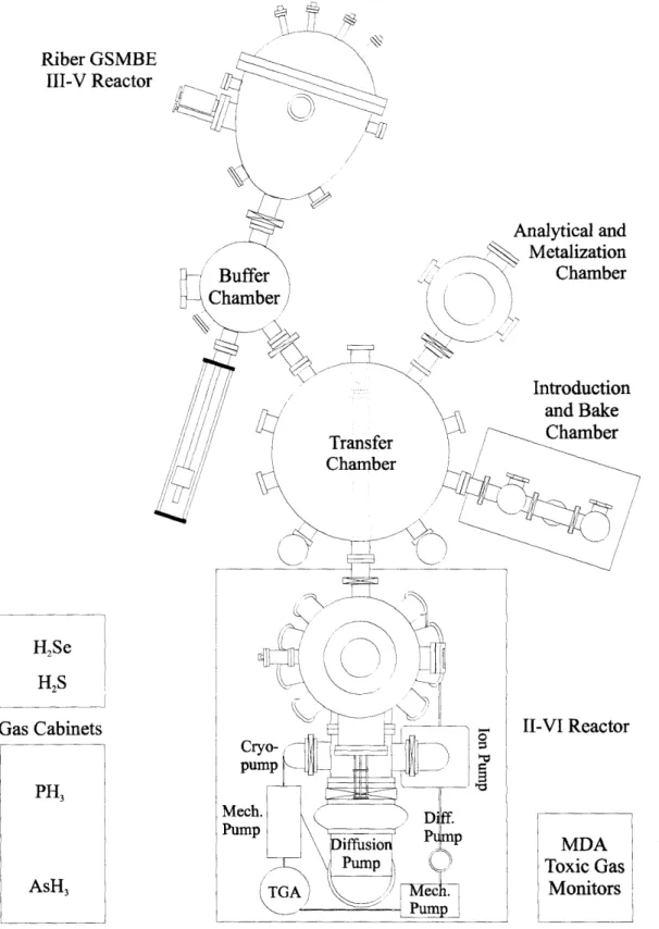
Figure 2.1 schematically shows the heteroepitaxial system in use at MIT for II-VI and III-V compound semiconductor growth. An ultrahigh vacuum (UHV) chamber connects with a GSMBE I-V system (Riber CBE32P) to a MBE II-VI system (custom built with parts from Emcore). The UHV transfer chamber allows for II-VI materials to be grown on III-V buffer layers, as described in this research.
Growth Preparation
All growths were performed on full 2" epi-ready GaAs wafers from AXT Crystal, Inc. The epi-ready GaAs wafer is first placed in a molybdenum block (which is previously baked at 4500C for two hours) and loaded into the introduction chamber (see figure 2.1). The sample is then moved via a mechanical arm in the transfer chamber to a bake station where it is baked at 2100C for one hour. The baking process reduces the water and adsorbed gases from the substrate prior to its introduction into the I-V system. After the bake, the sample is moved to the III-V growth chamber.
III-V GSMBE Growth
The growth of the III-V buffer layers is performed by GSMBE. GSMBE is based on the general principles of MBE as discussed above, but utilizes gaseous sources for the group V elements. Effusion cells are used for the group III elements (In, Ga, and Al) and are heated to temperatures of 7500C to 12000C, depending on the element. The group V elements are generated by "cracking" the hydride gases AsH3 and PH3. These hydrides, in conjunction with mass flow controllers (MFCs), simplifies the problem of flux control associated with the high vapor pressure elements As and P. The hydrides are thermally decomposed in a high temperature, low pressure cracker. The MFCs are used to precisely control the gas flow onto the substrate surface.
II-VI MBE Growth
In the II-VI system, a vacuum pressure of about 10'9 Torr is achieved by a
combination of four pumps: ion, cryogenic, diffusion, and a titanium sublimation pump. A reflection high energy electron diffraction (RHEED) (see appendix) screen is mounted in the center of the chamber to allow simple in-situ surface characterization. Eight 6" flange positions are available around the circumference of the reactor. Three positions are used for effusion ovens from EPI Corporation. These ovens contain elemental ultra-high purity (6N) Zn as the cation species, elemental (6N) Se as the anion species, and ZnC12 for Cl doping. For ZnSe growth, the Zn effusion cell is heated to about 3100C and the Se effusion cell is heated to about 190'C, which results in a flux
ratio of about Fzn/Fse = 0.7, as measured by a water-cooled crystal quartz oscillator. The quartz crystal oscillator is located about 2 cm below the substrate position.
Smaller flange ports contain an optical pyrometer, a CCD camera, and viewports to assist in sample manipulation. A nitrogen plasma source from Oxford Research (LN2 -cooled CARS25) is the p-type dopant source. The nitrogen flow into the reactor is controlled by a variable leak value. An RF power of approximately 350 W is used.
Neither Zn nor Se exhibits a unity sticking coefficient. Therefore, a unity flux ratio requires careful control of the material fluxes and the substrate temperature. Temperatures are measured simultaneously by a thermocouple and by a pyrometer. The
substrate temperature was calibrated with the Au-Ge eutectic transition (3560C). The
pyrometer emissivity was adjusted at the transition to yield an accurate reading. The offset of the thermocouple at this point was noted. All growth temperatures in this thesis refer to that of the calibrated pyrometer. Oscillations of the pyrometer temperature during growth provide a convenient and accurate technique for monitoring the ZnSe thickness.
Riber GSMBE III-V Reactor Analytical and Metalization Chamber Introduction and Bake Chamber H2Se H2S Gas Cabinets PH3 AsH3 II-VI Reactor MDA Toxic Gas Monitors
Figure 2.1: Schematic diagram of the MIT heteroepitaxial system: III-V GSMBE chamber, II-VI MBE chamber, and a UHV transfer chamber for II-VI/III-V growth.
2.4 N-Type Doping Using ZnCl2
As discussed previously, shallow n-type doping of ZnSe using ZnC12 has been in use since 1986 when a carrier concentration of 1x1019 cm-3 was achieved by heating a ZnCl2 effusion cell to 2500C during growth. In our laboratory, solid, anyhydrous ZnCl2 is used in an effusion cell to achieve n-type doping in ZnSe by MBE. The effect of the ZnCl2 cell temperature on the [Cl] concentration, as shown in figure 2.2, was determined
by secondary ion mass spectroscopy (SIMS) [22], which was performed by Charles Evans and Associates. 21 10 ' 1020 o 19 Q 10 118 Figure 2.2: [Cl]' 190 200 210 220 230 240 250 260
ZnC1, Effusion Cell Temperature (°C)
:rsus ZnCl2effusion cell temperature, as determined by SIMS analysis.
As seen in the semilogarithmic plot, with other parameters constant, chlorine concentration has an exponential dependence on the ZnCl2effusion cell temperature.
(00
.
^21
2.5 P-Type Doping Using an RFNitrogen Plasma Source
P-type doping of ZnSe-based materials proved to be much more difficult than n-type doping. The problems encountered in realizing low-resistivity p-n-type ZnSe films were due to compensation of acceptor impurities. For many years, this self-compensation was explained as the result of doping-activated native defects [23]. It is now thought that the mechanism for self-compensation of acceptors in ZnSe is the large atomic relaxation in the vicinity of acceptor impurities which affects the electrical properties of the material [24]. The realization of high-concentration p-type doping up to the 1018 cm"- range using nitrogen was made independently by Park et al. [3] and Ohkawa
et al [25]. 0 0 0
ZS
1020 1019 1018 4 n1 6 0 1 2 3 4 5 6 7 8 (x 10")Power*Pressure Product (W*Torr)
Figure 2.3: Incorporated nitrogen concentration, [N], as a function o Pressure (reproduced from ref. 22).
f RF Power * Gas
S S
The N concentration in ZnSe increases with both increasing RF power [26] and increasing aperture area of the plasma cell [27]. For the experiments described in this thesis, the doping concentration was determined from SIMS analysis of previously grown samples with differing RF power and aperture configurations. This data is reproduced in figure 2.3 (plot from ref. 17).
Chapter 3: Materials Design
3.1 Lattice Match
All things equal, growth of a lattice-matched layer is of higher quality than one that is lattice-mismatched. When the lattice constant of two semiconductors are matched, and the nucleation procedure is optimized, the epilayer can grow very smoothly, as shown in figure 3.1 below.
aepi=asub
asub
Figure 3.1: An epilayer grown on a lattice-matched substrate. The in-plane lattice constants of the two materials are equal.
Materials with different in-plane lattice constants behave differently. The inherent strain in a thick epilayer is released as misfit dislocations. However, since releasing strain as misfit dislocations requires energy, thin epilayers (pseudomorphic) will be totally elastically strained. At the critical thickness, the strain energy released by misfit dislocations equals the energy required to form the misfits. Beyond this critical thickness, misfit dislocations form, relaxing the strain in the layer.
The critical thickness is given by
h, = 4ab/f, b is the Burgers vector of the defect, a is a geometrical factor,f is the lattice-mismatch.
Figures 3.2 and 3.3 show a relaxed and a pseudomorphic epilayer grown on a lattice-mismatched substrate.
Figure 3.2: A relaxed epilayer on a substrate. epilayer is larger than that of the substrate.
a II =aepi asub
4-all=asub
a 11=asub
Figure 3.3: A pseudomorphic epilayer on a lattice-mismatched epilayer. The in-plane lattice constant of the epilayer is larger than that of the substrate, so, for thin layers, the lattice is strained to match the substrate.
3.2 (In,GaAI)P:
Lattice Constant:
Pre-Growth Calculations and Analysis
Calculations
Due to the formation of misfit dislocations at the ZnSe/GaAs interface as a result of the 0.27% lattice mismatch [28], a series of samples were grown with an additional
Misfit dislocation
The in-plane lattice constant of sub
InGaP buffer layer inserted between the GaAs and the ZnSe. With the proper composition, InGaP can be lattice matched to both GaAs and ZnSe.
By lattice-matching the InGaP buffer layer to the underlying GaAs buffer layer and to the overlying ZnSe layer, misfit dislocation in the ZnSe layer can be dramatically reduced. To achieve the high degree of lattice match necessary, the initial InGaP must be grown with the same in-plane lattice constant as GaAs, namely 5.653A and the final monolayers of InGaP must be grown with the same in-plane lattice constant as ZnSe, namely 5.668A.
The linear variation in lattice constant with respect to composition for such a ternary alloy is described by Vegard's Law. For Ini-xGaxP, this relation is given by:
a = 5.869 -0.418x
This relationship between lattice constant and mole fraction is shown in figure 3.4. U.5: InP 0.58
0.57
8
0.56 S 0.55 AlP, GaP 054n U. J-t 0 0.1 0.2 0.3 0.4 0.5 0.6 0.7 0.8 0.9 1.0 Mole fraction, xFigure 3.4: Lattice constant as a function of composition (reproduced from ref. 11).
As seen in the figure, the ternary alloys InGaP and InAlP both have a vs. x lines that pass through those of both GaAs and ZnSe, showing that these alloys can be
lattice-matched to GaAs and to ZnSe. By linearly grading this III-V buffer layer from the lattice constant of GaAs to that of ZnSe, the lattice mismatch between the III-V buffer layer and
II-VI layer can be minimized. The effect of a linearly-graded InGaP buffer layer is the formation of a misfit dislocation network that is uniformly distributed in the buffer layer. Due to this effect, dislocations are more spread out than in step-graded buffer layers, resulting in a larger degree of relaxation [29].
The alloy constant, x, of a III-V ternary layer is determined by the effusion cell temperatures and the hydride flow rates. A linearly-graded alloy composition can be obtained by stepwise linearly grading one of the effusion cell temperatures over the same time period as in the case of InGaP or InAlP.
The flux from an effusion cell can be determined experimentally by using reflection high energy electron diffraction (RHEED) oscillations. For GSMBE growth of
III-V materials, the temperature, and hence the flux, of the group III element is critical. Initially, the growth rate versus the temperature of the group III element is determined. The material's growth rate is simply related to the alloy fractions. The relevant equations for InGaP are:
tI' inGa Ga= 1In
%In = x',/lI jl . where r' is the rate of deposition in ýtm/hr.
Below are RHEED oscillations for the growth of GaAs and then for InGaP. Since the growth rate is limited by the group III elements, the deposition rate of Ga and (In,Ga) can be obtained from RHEED oscillations during the growth of GaAs and InGaP, respectively. At the onset of growth, one oscillation occurs for every deposited
monolayer. The growth rate is therefore calculated using the period of the oscillations, the lattice constant, and the time over which the oscillations are recorded.
24 sec 14 oscillations
Figure 3.5a: RHEED oscillations during growth of GaAs. r-IGa = 0.596 jim/hr.
5.5 sec 7 oscillations
From these plots, -1' -Ga '1Ga = 1.113 -0.596 = 0.517 jtm/hr = -1'I "- %In = 0.517/1.113 = 46%
InGaP lattice-matched to GaAs requires the indium mole fraction to be 0.49 and to be lattice-matched to ZnSe, the indium mole fraction must be 0.52. Thus, this sample had a lattice constant smaller than that of GaAs.
Lattice Constant: Analysis
The degree of lattice match between ZnSe and the underlying III-V buffer layer can be determined by x-ray double crystal diffraction (XRDCD, see appendix). When ZnSe is grown on a relaxed III-V buffer layer, it may be affected by strain in two directions. d1 is the spacing between the lattice planes in the direction perpendicular to the layer surface and dll is the lattice spacing within the planes. The degree of lattice-match, though, can be determined from the (400) XRDCD scan.
Figure 3.6a shows the x-ray rocking curve from a sample of ZnSe grown directly on a GaAs buffer layer. The peak on the left is due to diffraction off the ZnSe layer. The sharper, higher, peak towards the center is due to diffraction off the GaAs layer. The 350 sec separation between the peaks represents a lattice-mismatch of 0.27%, since both layers were grown to be fully relaxed.
Figure 3.6b shows the x-ray rocking curve from a sample of ZnSe grown on a graded III-V InGaP buffer layer. Diffraction from the InGaP layer begins at about -3500
2500 -2000
le (sec)
Figure 3.6a: layer. ZnSe
rve of 1 pm ZnSe grown on a GaAs buffer 400 sec. FWHMcGA, = 37 sec.
12000
10000 8000 6000 4000 2000 N -3500 -3000 -2500le
(sec)
ve of 1 pm ZnSe grown on a graded InGaP ak at -3200 sec. FWHMGaAs = 90 sec. 25000-20000 15000 rn 10000 5000 0 -3500 -1500 ____^ S I
z
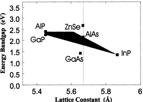
Energy Gap
A large amount of research on ZnSe LEDs has been done on ZnSe grown on GaAs substrates. However, the large valence band discontinuity results in the generation of an energy spike at the heterointerface. This spike acts as a barrier for hole conduction, and a voltage drop occurs.
It is possible to change the bandgap of a ternary or a quaternary semiconductor by changing the alloy's composition. Equations relating energy gap to composition at 300K have been calculated and can be found in several sources [30]. The equations for the direct energy gap (eV) of In,xGaxP and for In,.AlyP are given below.
In;,,GafP 1.351 + 0.643x + 0.786x2
In;,.AlP 1.351 + 2.23x
To provide both lattice match and a small valence band discontinuity to ZnSe, another degree of freedom is needed. These requirements have led to the research in the (In,Ga,Al)P material system as a buffer layer, as shown in figure 3.7.
To find a composition of (In,Ga,Al)P that is lattice-matched to GaAs, a region is formed by lines joining GaP, AlP, and InP. Any point directly vertical to GaAs will have the same lattice-constant as GaAs. Then, to obtain an energy gap between that of InGaP and that of InAlP, the ratio of the In, Ga, and Al concentrations are varied, while maintaining the GaAs lattice constant. In this case, an increase in the aluminum concentration increases the energy gap of the system. The precise ratio is calculated by mathematical equations which have been determined for a broad range of compounds.
3.5
S3.0
S2.5
S2.0
S1.0
0.5
5.4
5.6
5.8
6
Lattice Constant (A)
Figure 3.7: Energy bandgap (eV) versus lattice constant (a) for the (In,Ga,Al)P II-V material group and for GaAs and ZnSe.
Thus, the reason for research into the use of InGaAlP as a buffer layer is to obtain lattice-matching at both the GaAs and ZnSe interfaces as well as to minimize the valence band offset at these interfaces.
3.3 Nucleation
High quality growth of a semiconductor material by GSMBE or MBE requires a high degree of precision. Small deviations in effusion cell temperatures or fluxes result in drastic changes in the material's surface morphology. Too much or too little of one element yields an ensemble of dislocations. These dislocations have been thoroughly studied and described elsewhere [31]. Those that are most prevalent in ZnSe are shown and described below.
AlP
ZnSe
GaF
~.InP
GaAs:
II II SI I IPoor quality ZnSe growth is generally characterized by a large concentration of paired stacking faults bounded by Shockley-type partial dislocations. These dislocations are nucleated at or near the II-VI/GaAs interface. Figure 3.8a is a schematic of such a dislocation structure; figure 3.8b shows how the dislocation appears in plan-view TEM.
ZnSe
GaAs
Figure 3.8a: Schematic of a pair of stacking faults surrounded by Shockley dislocations nucleated at the GaAs/ZnSe interface.
/g,200
600 misfit dislocations arise due to the 0.27% lattice-mismatch between GaAs and ZnSe. These interfacial dislocations, as discussed previously, are introduced in ZnSe epitaxial layers in which the ZnSe thickness is larger than about 120 nm (the critical thickness of ZnSe) [32], to relax the misfit strain in the sample. Misfit dislocations appear in two forms, regular (straight) and irregular (zig-zag). It has been suggested that misfit dislocations form from dislocation half-loops which are nucleated at the film surface and glide along { 111
}
planes to the ZnSe/GaAs interface, where they form misfit dislocations [33]. The strain in the sample is directly related to the spacing between the 60' misfit dislocations, with large distances between misfits, suggestive of low strain. Figure 3.9 shows a plan-view TEM schematic of misfit dislocations.g220
Figure 3.9: Schematic of plan-view TEM image of misfit dislocations in a ZnSe/GaAs structure.
Finally, threading dislocations are a key problem in ZnSe-based devices. Dislocations form during growth due to differences in the thermal expansion coefficients of growth materials, introduction of substitutional impurities, and simply from non-ideal stoichiometry of the interface materials [34]. The GaAs substrate inherently has about 103 defects cm-2. Figure 3.10 schematically shows the formation of threading
103 defects cm-2. Figure 3.10 schematically shows the formation of threading
dislocations, in which stress has caused a column of atoms to slip out of place, resulting in the threading dislocation, or gap in the material.
0 0 0 0 0 0 0 0000000
0 0 0 0 0 0 0 slip plane
...
.-..
o..o..o. o.. 0o...
o ...
0 O0 000 0
00 0 0 0 00
4.1 ZnSe/(In,Ga,Al)P/GaAs: Effect of Bandgap Match
As discussed previously, growth of ZnSe on a graded layer of (In,Ga,Al)P has the potential of providing a lattice-matched, bandgap-matched structure. This structure would inherently have few misfit dislocations in the ZnSe layer, given the lattice-matched condition. By doping the (In,Ga,Al)P type with beryllium, and growing a layer of p-type ZnSe:N and then a layer of n-p-type ZnSe:C1, the EI-V layer could potentially provide a p-type ohmic contact to the ZnSe LED, eliminating the difficulty of obtaining an ohmic contact to p-type ZnSe. Figure 4.1 shows the effect on band offset that such a scheme is assumed to have.
Ec
Ev
Figure 4.1: Theoretical valence band offsets for the GaAs/ZnSe structure and the
GaAs/(In,Ga,Al)P/ZnSe structure. GaAs/ZnSe has a 0.96 eV valence band discontinuity;
InAlP/ZnSe has a 0.35 eV valence band discontinuity.
Chapter 4: Growth and Characterization
Ee
Initial growths of ZnSe/(In,Ga,Al)P/GaAs proved that the nucleation technique used in these growths was not ideal. Photoluminescence (PL) measurements [35] (see appendix) on these samples suggested that the ZnSe epilayers were of poor quality and were highly dislocated, primarily based on the intensity of the Yo feature, which is suggestive of extended defects [36]. Figure 4.2 shows the photoluminescence spectra of a sample of a 1ltm ZnSe epilayer grown on a layer of (In,Ga,Al)P, such that the III-V buffer layer is graded from the lattice constant of GaAs to that of ZnSe. The broad deep level luminescence band is indicative of a highly dislocated structure.
2.1 2.2 2.3 2.4 2.5 2.6 2.7 2.8 Energy (eV)
Figure 4.2: Photoluminescence scans of 1 Lm ZnSe grown on InAlP. The top figure shows the scan for pseudomorphic ZnSe (not relaxed). The bottom figure shows the scan for relaxed ZnSe with a deep level centered around 2.3 eV.
12 Fx Y 12 x50
Fx
_,J\Rz,
To verify and further analyze the InAlP/ZnSe structure, cathodoluminescence (CL) imaging was also performed (see appendix). This non-destructive technique allows the user to obtain a spatial map of the radiative and non-radiative recombination in a sample. The regions of radiative recombination appear bright; the regions of non-radiative recombination appear dark. Thus, threading dislocations appear as dark spots. Individual defects cannot be seen due primarily to the high diffusion constant of the electrons, and due to the sample being at room temperature.
CL scans were obtained for a group of five samples, each of which had the same basic structure of 1 pm MBE-ZnSe epilayers grown on 4pm relaxed GSMBE-(In,Ga,Al)P buffer layers on GaAs. In each case, the growth of ZnSe was initiated by simultaneously opening both the zinc and the selenium shutters. Table 4.1 shows the III-V buffer layers used for the samples and the lattice constants associated with each. The notation, aGaAs)aZnSe, refers to a layer of (In,Ga)P with an in-plane lattice constant graded from that of GaAs to that of ZnSe.
Sample # (In,Ga,Al)P Buffer Lattice constant, a
1 (In,Ga)P a = aGaAs
2 (In,Ga)P a = aGaAs" aZnSe
3 (In,Al)P a = aGaAs
4 (In,Al)P a = aGaAs"aZnSe
5 (In,Ga,Al)P a = aGaAs'aznse
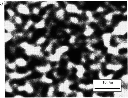
The CL images in figure 4.3 show the similarity between the radiative recombination in each of the described samples. The first image is of sample 2 (figure 4.3a), which has a III-V (In,Ga)P buffer layer that is graded from the lattice constant of GaAs to that of ZnSe. Such a structure should have a low density of misfit dislocations in the ZnSe. The image of sample 3 (figure 4.3b), which has an (In,Al)P layer with the lattice constant of GaAs, shows a very similar recombination structure to that of sample 2, even though this sample contains a 0.27% lattice-mismatch and includes aluminum at the III-V/II-VI heterointerface. Finally, sample 5 (figure 4.3c) is a lattice-matched (In,Ga,Al)P structure. The images of samples 3 and 5 look nearly identical, showing the small role that lattice match plays in the defect density of these samples, since sample 3 is lattice-mismatched and sample 5 is lattice-matched.
Figure 4.3a: CL of Sample #2--lCtm ZnSe on 4ptm relaxed graded layer of (In,Ga)P. T = 300K; Mag = 1700x.
5tm
Figure 4.3b: CL of Sample #3--lCtm ZnSe on 4ptm relaxed stepped layer of (In,Al)P. T = 300K; Mag = 1700x.
5 m
Figure 4.3c: CL of Sample #5--1itm ZnSe on 4jpm relaxed graded layer of (In,Ga,Al)P. T = 300K; Mag = 1700x.
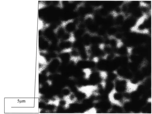
To determine the actual defect density for these structures, etch pit density measurements were performed (see appendix). The defect density in each of these samples was greater than 10' cm-2. Thus, initial CL characterization of ZnSe on lattice-matched (In,Ga,Al)P surfaces indicated the presence of an unexpectedly high density of dislocations. The origin of such a high density of defects was speculated to be due to the surface chemistry and to the ZnSe nucleation conditions.
An atomic force micrograph is shown in figure 4.4 for sample 5 (see appendix).
20
500 nm
Figure 4.4: Atomic force micrograph of l gm ZnSe film grown by MBE on 4jtm linearly graded (In,Ga,A1)P buffer layer. The mean roughness value over a 500 nm x 500 nm area was 4A.
Though the corresponding CL image of sample 5 shows a large percentage of non-radiative recombination, the AFM results are indicative of a very smooth growth front
based on the low Ra value (the mean value of the height of the sample's surface) of 4A. The lack of correlation between the defect density and the strain in the samples, however, suggests that the problem with these growths is primarily due to the details of the nucleation. Several ZnSe/GaAs nucleation studies have been recently reported [37].
4.2 ZnSe/GaAs: Effect of Nucleation
A nucleation study is complicated by the many factors involved. At a particular interface, each material can be rich in any one of its constituent elements. Growth of the overlying layer can begin after an exposure to any one of its elements. Thus, the (In,Ga,Al)P/ZnSe heterointerface has numerous nucleation possibilities. To simplify the situation, the ZnSe/GaAs nucleation process can be studied first, to determine the ideal growth parameters in terms of the defect density of the overlying ZnSe. Then this structure, using a very thin layer of GaAs, can be grown on a graded (In,Ga,Al)P buffer layer. In this way, the lattice-match afforded by an (In,Ga,Al)P buffer layer can be used, while taking advantage of the previously studied ZnSe/GaAs nucleation. A very thin, pseudomorphic layer of GaAs will be strained to maintain the lattice constant of the underlying (In,Ga,Al)P.
GaAs
GaAs can be terminated such that it is either Ga-rich or As-rich, and the percentage in each case may be intentionally varied. These different terminations create different GaAs surface reconstructions, which can be monitored by RHEED (see appendix).
different GaAs surface reconstructions, which can be monitored by RHEED (see appendix).
All of the GaAs was grown at a substrate temperature of 6000C, as determined by
an optical pyrometer. After the growth of the buffer layer at 6000C , the surface exhibited an As-stabilized (2x4) reconstruction. As the substrate temperature decreased to 5300C with the sample exposed to an As flux, the (2x4) surface reconstruction changed to a c(4x4) reconstruction. This reconstruction remained stable even after the arsine flow into the chamber was terminated at 3500C. To prepare a buffer layer exhibiting a (2x4) reconstruction at room temperature, the substrate temperature and the As flux were simultaneously lowered after growth. The arsine flow was reduced to 0.1 sccm, which was sufficient to maintain the (2x4) reconstruction. The RHEED pattern was closely monitored during this process, as seen by the similarity of the post-growth (2x4) RHEED patterns at a high and a low temperature in figure 4.5.
fore transfer (Tc=2700C).
surface coverage; the (2x4) figure 4.6. (Top View)
S
o*
010
0
00000;ROO 0'0
0
00
0 00
0
O 00
0 0 040
*
o
1
.ot .o0
~oWeo~
(Side View)I GaAs (100% arsine surface coverage). (reproduced from ref. 38)
a
D
DD
D
Figure 4.6a: Top view and side view of c(4x4)-reconstructed GaAs (100% arsine surface coverage). (reproduced from ref. 38)
(Top View) (Side View) As Ga As Ga
Figure 4.6b: Top view and side view of (2x4)-reconstructed GaAs (75% arsine surface coverage). (reproduced from ref. 38)
ZnSe
ZnSe can be grown in several ways on the GaAs underlayer. Growth may include
a pre-exposure of either Zn or Se, for varying periods of time. Another technique that has
been studied over the past few years for ZnSe growth is Migration-Enhanced Epitaxy
(MEE) [39]. MEE involves alternately chopping the beams produced from the effusion cells in a cyclic fashion. One cycle of MEE represents one opening of each shutter.
Many variables are involved in MEE-each shutter must be opened long enough to fill
all surface sites (to allow a full monolayer of the element to form on the surface) and enough time must be allowed in the interim between shutter openings to ensure that the
previously deposited atom finds an energetically favorable site to incorporate into the
AEv = 0.62 eV AEv = 1.59 eV
AEV= 1.17 eV AEv = 1.05 eV
[110] L=As D=Se o=Ga *=Zn
[001]
Figure 4.7: Surface configurations for ZnSe on GaAs. The trend in band offsets is based on theoretical analysis.
lattice. MEE increases the atom mobility on the surface by allowing time for surface diffusion prior to incorporating. This technique has been investigated in this study.
ZnSe/GaAs
The surface stoichiometry for the growth of ZnSe on GaAs can be varied in many ways, as discussed above. One way to vary the surface chemistry is to change the surface reconstruction pattern of the III-V buffer layer. Another means of varying the surface chemistry is to start the ZnSe growth with a pre-exposure of zinc or selenium atoms.
Figure 4.7 shows several possible surface configurations, each corresponding to a different valence band offset between the ZnSe and the GaAs, with the GaAs having a higher valence band energy, hindering hole injection into the II-VI layer in a ZnSe-based LED structure. The trend in the band offsets, based on theoretical analysis, is related to the establishment of neutral interfaces with different atomic configurations [40].
The top two configurations can result from 1:1 compositions of gallium to arsine and zinc to selenium at the interface. The lower left configuration shows an arsine-rich GaAs surface and a zinc-rich ZnSe growth start. The lower right configuration shows a gallium-rich GaAs surface and a selenium-rich ZnSe growth start.
Thus the variety of possible nucleation processes is evident, even for the seemingly simple growth of ZnSe on GaAs.
MBE-ZnSe/c(4x4)-reconstructed GaAs
The first set of growths involved ZnSe grown on c(4x4)-reconstructed GaAs, with and without pre-exposures of Zn and Se. The table below details the growths.
Sample # GaAs Buffer? Pre-Exposure? Pre-Exp Time
6 Yes Se 1 min
7 Yes Zn 2 mins
8 Yes No
Table 4.2: Pre-exposures used in MBE-ZnSe/c(4x4)-reconstructed GaAs growths
These growths were intended to primarily give information about the effect of the various nucleation techniques on the defect densities in the overlying ZnSe. Therefore, the growths were primarily characterized by CL and EPD. Figure 4.8 shows the CL images for each sample. Each has an estimated defect density of over 107 cm 2, as determined both by CL and by etch pit measurements.
Figure 4.8: (a) MBE-ZnSe/c(4x4)-reconstructed GaAs with Zn and Se shutters opened simultaneously; (b) MBE-ZnSe/c(4x4)-reconstructed GaAs with a 2 minute Zn pre-exposure; (c) MBE-ZnSe/c(4x4)-reconstructed GaAs with 1 min Se pre-exposure.
Though the contrast in these three images differs, the percentage of radiative to non-radiative recombination seems nearly identical. This suggests that the c(4x4)-reconstructed GaAs surface results in a high defect density (> 107 cm-2), regardless of the pre-exposure before the MBE-ZnSe growth.
Another means of characterizing the effects of the nucleation conditions is the use of atomic force microscopy (AFM) (see appendix). Figure 4.9 shows the atomic force micrograph from a sample of ZnSe grown on c(4x4)-reconstructed GaAs with a two minute Zn pre-exposure. A mean roughness (RI of 9A was measured over a 500 nm x 500 nm area.
Figure 4.9: Atomic force micrograph of 1 ýtm ZnSe film grown by MBE on a Zn pre-exposed c(4x4)-reconstructed GaAs buffer layer (sample 7).
MBE-ZnSe/(2x4)-reconstructed GaAs
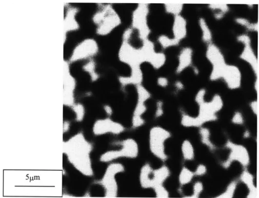
The second set of growths involved ZnSe grown on (2x4)-reconstructed GaAs, with two minute pre-exposures of Zn (sample 9). This same structure was grown twice to strengthen the validity of the results. Figure 4.10 shows the CL image obtained from this sample.
The CL image of this sample shows that the growth of ZnSe on (2x4)-reconstructed GaAs results in a much lower density of defects than for the growth on c(4x4)-reconstructed GaAs. This is clear by the decreased percentage of dark areas, which are representative of non-radiative recombination sites. The dark area in the upper left portion of the image is the result of the sample mount.
~ ~
Figure 4.10: Room temperature CL image of MBE-ZnSe/(2x4)-reconstructed GaAs with a 2 min Zn pre-exposure (sample 9); Mag=1700x.
AFM was also performed on this sample and the results are shown in figure 4.11. The mean roughness (I) value was 7A over a 500 nm x 500 nm area, lower than that found for ZnSe grown on a c(4x4)-reconstructed GaAs buffer layer.
In other sets of similar films, the R, values from the ZnSe epilayer grown on c(4x4)-reconstructed GaAs were consistently larger than the values measured from the ZnSe epilayers grown on (2x4)-reconstructed GaAs.
Etch pit density (EPD) measurements of ZnSe grown on (2x4)-reconstructed GaAs reveal an EPD of less than 106 cm-2, a factor of ten lower than that of ZnSe grown on c(4x4)-reconstructed GaAs.
Reduced defect densities in ZnSe epilayers grown on (2x4)-reconstructed GaAs agrees with another recent study [41]. The complexity of the ZnSe/GaAs interfacial layer makes it difficult to isolate the reason for the reduced defect density in ZnSe grown on (2x4)-reconstructed GaAs surfaces compared to ZnSe grown on c(4x4)-reconstructed GaAs surfaces. A contributing factor for the difference is that a more charge neutral interface is formed on a (2x4)-reconstructed GaAs surface as opposed to a c(4x4)-reconstructed GaAs surface. A completely charge neutral interface can be formed if the anion plane is 50% As and 50% Se. (2x4)-reconstructed GaAs has, on average, a 75% As surface coverage, which is lower than the 100% surface coverage of c(4x4)-reconstructed GaAs [42].
20 nm
500 nm
Figure 4.11: Atomic force micrograph of 1 }.m ZnSe film grown by MBE on a Zn pre-exposed (2x4)-reconstructed GaAs buffer layer (sample 9).