Design and Test of a 94 GHz Overmoded
Traveling Wave Tube Amplifier
by
c(D LC) l LU~~ iOLU- Cf) <~ :~UL
E
co
< 0or -ClElizabeth J. Kowalski
B.S. Electrical Engineering, the Pennsylvania State University (2008)
S.M. Electrical Engineering and Computer Science, Massachusetts
Institute of Technology (2010)
Submitted to the
Department of Electrical Engineering and Computer Science
in partial fulfillment of the requirements for the degree of
Doctor of Philosophy
at the
MASSACHUSETTS INSTITUTE OF TECHNOLOGY
February 2015
@
2015 Massachusetts Institute of Technology. All rights reserved.
Signature redacted
A u th o r .... ...
Department of Electrical Engineering and Computer Science
December 31, 2014
Certified by...Signature
redacted
Richard J. Temkin
Senior Research Scientist, Department of Physics
Thesis Supervisor
Accepted by ...
Signature
redacted
/ Prif isor Leslie A. Kolodziejski
Chairman, Committee on Graduate Students
Department of Electrical Engineering and Computer Science
Design and Test of a 94 GHz Overmoded Traveling Wave
Tube Amplifier
by
Elizabeth J. Kowalski
Submitted to the Department of Electrical Engineering and Computer Science on December 31, 2014, in partial fulfillment of the
requirements for the degree of Doctor of Philosophy
Abstract
This thesis discusses the design and test of an overmoded W-band Traveling Wave Tube (TWT). The TWT was designed to operate in the rectangular TM3 1 cavity
mode at 94 GHz. The unwanted lower order, TM 1 and TM2 1, modes were suppressed
using selectively placed aluminum nitride dielectric loading. Simulations in 3-D CST Particle Studio confirmed suppression of unwanted modes due to dielectric loading and operation in the TM3 1 mode. The TWT was designed to operate at 31 kV with
310 mA and a 2.5 kG solenoid magnet. Simulations in both 1-D Latte and 3-D CST
predicted 32 dB of gain, 200 MHz bandwidth, and 300 W peak output power for the TWT at 94 GHz. Test structures of 9- and 19- cavities were made via CNC direct machining. Cold test measurements showed suppression of the unwanted modes and transmission of the TM3 1 mode, which correlated well with HFSS simulations. Two
final 87-cavity structures were built and cold tested.
The experiment was designed and built in-house at MIT (with exception of the electron gun cathode, manufactured by industry). It was operated with a 3 microsec-ond pulsed power supply. A beam test was implemented which confirmed operation of the TWT set up and electron gun. The electron gun operated at 31 kV with 306 6 mA of current detected at the collector and 88 % transmission of current. Initial operation of the TWT showed zero-drive stable operation and demonstrated 8 dB of device gain and 10 W peak output power at 95.5 GHz. Following these first tests, the magnetic field alignment was improved and the second structure, which showed better circuit transmission in cold test, was installed. The overmoded TWT produced 21 2 dB device gain (defined as P0,t/Pi,) at 94.3 GHz and 27 W of saturated output
power in zero-drive stable operation. The TWT was estimated to have about 6 dB of additional loss due to coupling into and out of the circuit. Taking that loss into account, the gain on the TWT circuit itself was estimated to be 27 2 dB circuit gain.
CST simulations for the experimental current and voltage predict 28 dB circuit gain,
in good agreement with measurements.
This experiment demonstrated the first successful operation of an overmoded TWT. The overmoded TWT is a promising approach to high power TWT
opera-tion at W-Band and to the extension of the TWT to terahertz frequencies.
Thesis Supervisor: Richard J. Temkin
Acknowledgments
This thesis would not have been possible without my advisor, Dr. Richard J. Temkin. Always willing to help, offer advice, and teach the finer points of vacuum electronics, he guided me through this project and helped to make my PhD successful. Every member of the Waves and Beams Group in the PSFC also helped me in my research. Particularly, my officemates Dr. Emilio Nanni and XueYing Lu dealt with my dis-tracting conversation, pungent teas, and research woes. Ivan Mastovsky's expertise helped my experiment to be operational, while Dr. Michael Shapiro ensured that my theory and simulations were correct. In addition, Dr. Sudheer Jawla, Dr. David Tax, Dr. Brian Munroe, Jason Hummelt, JeiXi Zhang, Sam Schuab, Alexander Soane, and Haoron Xu all offered their advice and help, from Friday evening brainstorming to unexpected company in the lab on Saturday.
Graduate Women at MIT, GWAMIT, helped me to realize I was not alone in my endeavors and introduced me to some amazing women at MIT who encouraged me and became great friends. It was amazing to be a part of shaping GWAMIT, and I hope that the organization continues to grow in the future.
Of course, my family and friends helped me through the long nights, weeks,
months, and years of research. My parents taught me how to learn, and my sis-ters taught me how to have a life. My husband, Edward Loveall, provided endless support. He listened to me practice countless presentations, so he may even under-stand 31 % of this thesis.
Elizabeth Kowalski Cambridge, MA December 22, 2014
to Edward
onion ('anyan) noun. An edible bulb with
a pungent taste and smell, composed of several concentric layers, used in cooking.
Contents
1
Introduction
21
1.1 M otivation . . . . 21
1.2 A Brief History of TWTs . . . . 29
1.2.1 Vacuum Tubes and Radar . . . . 29
1.2.2 Invention of the TWT . . . . 32
1.2.3 More Vacuum Devices . . . . 35
1.3 Modern Day W-Band Vacuum Tubes . . . . 36
1.3.1 W-Band TWTs . . . . 36
1.3.2 Other W-Band Devices . . . . 38
1.3.3 Overmoded TWTs . . . . 39
1.4 Overview of Thesis . . . . 40
2 Theory of Traveling Wave Tubes 41 2.1 TWT Overview . . . . 41
2.2 Electron Beams in Vacuum Tubes . . . . 44
2.2.1 Pierce Electron Gun . . . . 44
2.2.2 Magnetic Field Confinement . . . . 51
2.2.3 C ollector . . . . 53
2.3 Analytical Theory for Slow-Wave Structures . . . . 53
2.3.1 Gain in the Circuit . . . . 59
2.4.1
Helical TW Ts . . . . ...
.. . . . .
.
63
2.4.2 Coupled-Cavity TWTs . . . . 65
3 Design of a 94 GHz Overmoded Coupled-Cavity TWT 69 3.1 Problem Statement ... ... 69
3.2 Electromagnetic Cavity Design ... ... 70
3.2.1 Cavity Fields ... ... 71
3.2.2
The TM
31M ode
...
.
73
3.2.3 Other Modes and Dielectric Loading . . . . 76
3.2.4 Final Design Parameters . . . . 81
3.2.5 Other Design Considerations . . . . 89
3.3 Analytical Calculations and Simulations . . . . 91
3.3.1 Pierce TWT Analytical Theory . . . . 91
3.3.2 3-D CST Simulations . . . . 94
4 Cold Tests of the Overmoded TWT Circuit 99 4.1 Machining Techniques and Tolerances . . . . 99
4.2 Low Power Cold Test Measurements . . . . 103
4.2.1 M aterials . . . . 103
4.2.2 Dielectric Loading . . . . 110
4.3 87-Cavity Design Cold Test Results . . . . 112
5 Experiment Design and Set-up 119 5.1 Experiment Overview . . . . 119 5.2 Solenoid M agnet . . . . 122 5.3 Electron G un . . . . 125 5.3.1 D esign . . . . 126 5.3.2 M anufacturing . . . . 130 5.4 D riving Sources . . . . 133
5.4.1
94 G H z EIO . . . .
133
5.5
RF Vacuum Windows
...
136
5.6 High Power Pulse Modulator ...
138
5.7 Safety Interlock System and Controls . . . .
141
5.8 Installation . . . .
143
6 Experiment Results 147 6.1 Electron Gun Beam Test . . . . 147
6.2 94 GHz TWT - Structure A . . . . 151 6.2.1 Full D ielectric . . . . 151 6.2.2 H alf D ielectric . . . . 156 6.3 94 GHz TWT - Structure B . . . . 157 6.3.1 R esults . . . . 157 6.3.2 A nalysis . . . . 162 7 Conclusions 171 7.1 Summary of Results . . . . 171 7.2 Discussion of Relevance. . . . . 173 7.3 Future W ork . . . . 174
The Haystack Observatory 94 GHz antenna. . . . . Average output power vs. frequency for vacuum and solid state devices.
1-3 Transmission (%/km) vs. frequency for sea-level conditions. Examples of electronic warfare usages [1]. . . . . The U. S. Military Active Denial System. . . . . Early vacuum tubes diagrams. . . . . Drawings of the first TWT design. . . . . A diagram of the first TWT experiment and John Pierce. .
A block diagram overview of a TWT amplifier circuit. . . . .
The i-directed electric field in the TWT. . . . . Diagrams with different anode-cathode configurations .. . . . . A diagram showing the ideal design of a Pierce electron gun... The electron beam compression and magnetic field confinement. The space charge reduction factor, R vs. eb. . . . .
B vs. non-synchronous parameter, b, for various conditions. . . . . .
The helical TWT slow-wave structure. . . . . A folded waveguide coupled-cavity design. (Picture from [37].) . . . A rectangular folded-waveguide coupled-cavity TWT. . . . . The dispersion relation and period length for a coupled-cavity TWT.
List of Figures
1-1 1-2 22 23 . . . . 25 . . . . 26 . . . . 27 . . . . 30 . . . . 32 . . . . 33 1-4 1-5 1-6 1-7 1-8 2-1 2-2 2-3 2-4 2-5 2-6 2-7 2-8 2-9 2-10 2-11 42 43 47 49 49 57 62 63 65 6566
3-1 An illustration of the electric and magnetic fields in the TM1 1 0 cavity
mode. (Figure modified from [121.) . . . . 72 3-2 Contour plots of the electric field, E2, for the lowest order cavity modes. 74
3-3 Two cavities of the TWT structure linked via staggered coupling slots, as seen with an isometric view and from the top of the structure. . . 75
3-4 The electric field patterns of the three lowest order TM modes in a rectangular cavity tuned to 94 GHz for the TM31 mode. . . . . 77
3-5 The dispersion relation for the lowest order TM modes of the cavity. . 78 3-6 Placement of dielectric on the top and bottom of the cavity. . . . . . 79 3-7 The electric field patterns of the three lowest order TM modes in a
rectangular cavity. . . . . 80 3-8 The transmission through a single cavity with and without dielectric
loading for the lowest four TM modes. . . . . 81 3-9 Simulation results showing the variation of current, K, and C as
de-pendent on cavity parameters. . . . . 82 3-10 The effect of beam tunnel size on calculated coupling impedance through
the m iddle of the circuit. . . . . 83 3-11 IO/V ratio vs. operation voltage, Vo, for different electron beam radii. 85 3-12 The final cavity design showing the dielectric loading and
manufactur-ing fillets. . . . . 86 3-13 The dispersion relation for the first three cavity modes of Design A, as
calculated by HFSS.
. . . .
87
3-14 The coupling impedance and dispersion relation for the TM3 1 mode of
D esigns A and B . . . . 88 3-15 The input coupler from standard waveguide into the first cavity of the
T W T . . . . 90 3-16 Linear gain vs. operation voltage for 94 GHz operation and design
parameters discussed in Table 3.2. . . . . 93 3-17 Linear gain vs. frequency for LATTE simulations. . . . . 93 3-18 The full 87 cavity structure with dielectric loading as simulated in CST. 95
3-19 Power out vs. time for a 90 mW input signal along with an FFT of the
output signal. . . . . 95
3-20 The energy of the particles in the beam tunnel at the end of the circuit, and the particle density along the length of the cavity. . . . . 96
3-21 Output power vs. input power for the simulated TM3 1 coupled-cavity T W T . . . . 97
4-1 The assembly of 4-plate and 2-plate 9-cavity cold test structures. . . . 101
4-2 HFSS simulations showing a WR-08 waveguide with gaps at the top, mid-plane, and bottom of the waveguide. . . . . 102
4-3 CAD drawings and machined 9- and 19-cavity cold test structures. . . 104
4-4 The measured transmission through (a) 9- and (b) 19-cavity OFHC copper structures compared to HFSS simulations. . . . . 105
4-5 The measured transmission through (a) 9- and (b) 19-cavity glidcop structures compared to HFSS simulations. . . . . 106
4-6 The measured transmission for copper cold test structures. . . . . 108
4-7 The measured transmission for glidcop cold test structures. . . . . 109
4-8 Detailed pictures of the final 87-cavity structure. . . . . 113
4-9 Transmission measurements for the first 87-cavity structure (A). . . . 114
4-10 Transmission measurements for the first 87-cavity structure (A) with dielectric loading . . . . 115
4-11 Transmission measurements for Structures A and B with no dielectric load ing . . . . . 116
4-12 Transmission measurements for the assembled structures that under-w ent hot test. . . . . 116
5-1 The full experimental set up. . . . . 120
5-2 A rendering of the TWT tube assembly inside of the solenoid magnet. 121 5-3 The 2.5 kG solenoid magnet installed for testing. . . . . 122
5-4 Poisson calculation of the solenoid electromagnet. . . . . 124
5-6 The 2-D cylindrical electron gun geometry. . . . . 126
5-7 The beam envelope calculated via Michelle . . . . . 127
5-8 The equipotential lines and particle trajectories as calculated by Michelle. 128 5-9 The electric field in the electron gun for operation at 31 kV. . . . . . 129
5-10 A cross-sectional view of the electron gun modeled in Autodesk Inven-tor with cold dim ensions. . . . . 131
5-11 Pictures of the electron gun and beam test assembly. . . . . 132
5-12 A picture of the 94 GHz EIO. . . . . 134
5-13 Frequency vs. power for the Millitech AMC. . . . . 135
5-14 Measured and calculated transmission through the RF windows. . . . 137
5-15 One of the fused silica RF windows in a 2-3/4 con flat flange, installed on the TWT. The input WR-28 waveguide can be seen . . . . 138
5-16 A block-diagram of the PFN and high voltage pulse transformer set-up with dual-experiment access. . . . . 139
5-17 The modulator set-up of the TWT experiment. . . . . 140
5-18 An electronic schematic of the high voltage pulse transformer and TWT experim ent. . . . . 141
5-19 The control system for the experiment and safety interlock system. . 142 5-20 Installation of the TWT structure onto the anode. . . . . 143
5-21 Installation of the WR-10 90 degree waveguide bends and support structures into the tube. . . . . 144
5-22 Completion of installation for the TWT experiment. . . . . 145
5-23 The fully assembled TWT experiment. . . . . 146
6-1 A cross-sectional rendering of the beam test experiment. . . . . 148
6-2 Sample voltage and collector current measurements from the beam test. 149 6-3 The Child-Langmuir curve for the electron gun. . . . . 150
6-4 Device gain (and output power) vs. input power observed at 95.5 GHz w ith V7 = 27 kV . . . . . 152
6-5 Sample traces of the collector current and output power measurements for Structure A . . . . 154 6-6 Device gain vs. bandwidth for operation at V=27 kV. . . . . 155 6-7 Device gain and output power vs. input power, showing 20.9 dB linear
g a in . . . . 158
6-8 Circuit gain in the TWT as compared to simulated gain. . . . . 160 6-9 Device gain vs. frequency in the TWT for two different operation points. 161 6-10 The diagnostic measurements for high-gain operation at 94.27 GHz. . 163 6-11 The diagnostic measurements for saturated power operation at 94.26
G H z . . . . 165
6-12 The diagnostic measurements for an oscillation observed during the start of operation. . . . . 167
List of Tables
3.1 Dimensions of Final Structure . . . . 87 3.2 TWT Operation Parameters . . . . 92
Chapter
1
Introduction
1.1
Motivation
In this technology-dependent world, electromagnetic applications are present in our everyday lives. Household microwave ovens, commercial cell phone communications, radar, satellites, and advanced military capabilities are just a few of the varied ways that electromagnetic waves are used. For the most part, these applications exist at low frequencies and low powers where solid state transistors and other devices are able to satisfy the needs of the applications. Advances to higher frequency bands require the development of new devices at those frequencies. Currently, there are few devices which are capable of operating in the regime of high-frequency and high-power. Vacuum electronics are extremely useful for high power applications, but extending these devices to high frequencies is difficult for reasons that will be explored. As we expand our scientific knowledge, applications are available at high frequencies and for higher powers, but they require devices for practical implementation which don't yet exist.
The need for both higher power and higher frequency devices for millimeter wave, microwaves, and terahertz waves is easily understood by looking at radar and com-munications systems. Simply put, operating with higher powers means that we can communicate over longer distances. In addition to power, we must consider the band-width of communication, i.e. the range of frequencies over which a transmission can
(a)
(b)
Figure 1-1: The Haystack Observatory 94 GHz antenna. Two sets of simulated data
show a satellite that has been imaged with (a) 2 GHz or (b) 4 GHz bandwidth [11].
occur. Operation at higher frequencies means that larger bandwidths are available to
transmit data, leading to higher resolution imaging. For example, Haystack Radar,
shown in Figure 1-1 is a radar system located in Westford, MA that is used for space
tracking, communications, and astronomy. The system originally operated at 10 GHz,
and was recently upgraded to have a second operation point at 94 GHz. The
band-width available at 94 GHz can be as large as 4 GHz. The figure shows the simulated
detection of a satellite by the Haystack radar via two different operation bandwidths
for comparison [11]. It's easily observed that more details can be seen with a larger
bandwidth. Operation at 94 GHz allows for this large bandwidth to be achieved and
for details to be resolved which would not otherwise be detected.
Space communications also benefit from large bandwidths due to large distances
requiring long transmission times. NASA has built most of their communications
systems around 10 GHz, like those on board the Mars Curiosity Mission, because it
has a relatively high bandwidth for communication and reliable, high power devices
are available to operate at that frequency.
Some NASA missions, like the Mars
Reconnaissance Orbiter, operate at higher frequencies, about 32 GHz, in order to
support higher bandwidths and higher data rates
[47].
It is likely that future NASA
0 0. (U
10
106
10 5 10 3 10 210
1
10-10-2
10
0001
0.001
0.01
0.1
Frequency (THz)
1
10
Figure 1-2: Average output power vs. frequency for vacuum and solid state devices.
This graph demonstrates the THz gap, from 0.3-10 THz, a frequency range for which
no or limited devices exist. Figure adapted from [23].
missions will be at even higher frequencies for better communications; but reliable,
high power, devices must exist at those frequencies first.
Many more applications for high power, high frequency devices exist, but all
electromagnetic applications are limited by our abilities to produce and amplify
elec-tromagnetic signals at the frequency of operation. At low frequencies, high power
sources and amplifiers are readily available. However, at higher frequencies there
is an undeniable need for reliable, high-power, and cost-effective power sources and
amplifiers.
Unfortunately, there is a range of frequencies with radar and communications
applications for which there are no viable devices which offer high output powers.
Figure 1-2 displays the power limits of electronic devices as they depend on frequency.
Solid state and vacuum electronic devices provide a wide range of available power for
diverse applications below 1 GHz. Vacuum electronics are robust and able to provide
higher power at frequencies up to 100 GHz (and even higher). In general, vacuum
cacuum
Devices
Gyrotron
Klystron
Gridded Tubes]
I\ CFA
Helix TWT
TWVT
BT
FETBW
Solid State
J
Devices\
impAT
devices are less desirable because they can be large, complex systems. However, their ability to provide high power makes them viable options for certain applications. For all electronic devices, the relative size of interaction circuits inversely scales with frequency. At high frequencies, above 300 GHz, the small wavelengths of operation severely limit the types of devices that can perform at high powers. At even higher frequencies, above 10 THz, laser photonic devices are able to provide high power for applications in the visible light spectrum, x-rays, and gamma-rays. These devices have wavelengths less than 30 micrometers. The output power for devices such as quantum-cascade lasers drops off rapidly at frequencies lower than 100 THz due to physical limitations at relatively large wavelengths of operation [63]. In addition to vacuum devices, quantum-cascade lasers in the THz range of frequencies are a large area of interest.
At present, the two opposing frequency limits between electronic and photonic devices leads to the range of frequencies for which there are no high power devices. The range is between 300 GHz and 10 THz and is referred to as the terahertz gap. In this gap there is very limited power output from all types of devices. Though, many vacuum electron devices have recently been able to output relatively high power in this frequency range. Recent experimental achievements with gyrotrons, klystrons, and Traveling Wave Tubes (TWTs) have demonstrated that vacuum electronics are able to perform well in the Terahertz Gap, though limitations in power output still exist in all types of devices [5]. The characteristics and benefits of these devices will be described in the next section.
For practical applications, several frequency ranges, referred to as "windows" or "bands," are commonly used in communications and are the subject of research de-velopments. These bands take advantage of the earth's atmospheric conditions, as shown in Figure 1-3, which shows the transmission associated with an electromag-netic wave traveling through the earth's atmosphere. They are called "windows" since they refer to a range of frequencies that can be "seen", or transmitted, through the atmosphere. The ability of a certain frequency to transmit changes due to several atmospheric factors, but, for simplicity, sea level conditions with moderate humidity
- 100 C U) -C CL 0 60-E ,: 40- -.0 U) E 20 C 50 100 150 200 250 300 350 Frequency (GHz)
Figure 1-3: Transmission (%/km) vs. frequency for sea-level conditions. The black dotted line indicates the atmospheric window at 94 GHz.
were assumed in calculation. Several frequency windows can be seen in Figure 1-3 where there are transmission peaks in the atmosphere. Resonances in the atmosphere, which absorb large quantities of electromagnetic waves leading to transmission dips at certain frequencies, are due to molecules in the air. In the frequency range shown in the figure (0-350 GHz), oxygen and water particles dominate the loss effects. Atmo-spheric losses- are dependent on a wide variety of conditions that affect the molecules in the air, most importantly weather conditions and altitude, but the windows of
low losses shown in the figure are still the best transmission frequencies to use in communication applications [59]. The low loss windows can also be referred to as high transmission bands, i.e. it takes less power to transmit electromagnetic waves at those frequencies for longer distances than at the resonance frequencies. In addition, higher frequencies have larger windows, allowing for larger operation bandwidths at those frequencies.
Several systems and agencies have built communications infrastructure in the frequency bands that have low losses in atmosphere. At 94 GHz there is a large window of communications that is often associated with air force communications and many developments in vacuum devices have been aimed at developing high power tubes for use in that frequency range. In addition, there is a window at 220 GHz which is also an area of large development for communications due to the large bandwidth
J
Figure 1-4: Examples of electronic warfare usages [1].
that is possible. These high frequency windows are also in use for weather research
due to atmospheric transmission characteristics, the small wavelength of operation,
and the large bandwidth available. These two bands at 94 and 220 GHz are below
the defined Terahertz Gap in frequencies, and vacuum tubes exist which provide
useful output powers. However, high power devices are still in development at these
frequencies due to a need for more power than is currently accessible and a desire
for cheaper alternatives. It is also relevant that development of devices at these
frequencies will lead to more robust devices that can be modified for use at even
higher frequencies in the following years.
Just below the Terahertz Gap is a band of frequencies known as the W-band,
between 75-110 GHz, for which there are many applications. This range includes
the 94 GHz transmission window in atmosphere. The possibility of high data rates
and the crowding of communications at lower frequencies make the W-band a good
communications channel. Though no commercial systems exist in the W-band yet,
many research and military applications are already implemented. The Haystack
Radar, shown in Figure 1-1 takes advantage of the transmission window in order to
image objects in space. Gyrotron devices are used to power the system since they
Figure 1-5: The U. S. Military Active Denial System, which operates at 95 GHz. A
humvee is necessary to move the equipment.
can provide the necessary high powers and bandwidths that are needed for operation.
Figure 1-4 shows electronic warfare applications, such as a frequency jammer, which
involves disrupting electronic systems with high power microwave and millimeter wave
signals. These applications require very high power devices to disrupt appropriately
and from a safe distance. There are many other communications capabilities that
exist at 94 GHz, many involve devices installed on satellites and airplanes. As such,
it is often necessary that the devices are robust, reliable, light weight, and have long
operation life-times. Traveling Wave Tubes (TWTs), which will be discussed in the
next section, satisfy these requirements.
Besides communications there are, of course, several other applications in the
W-band of frequencies. Passive imaging systems to detect concealed weapons typically
operate around 94 GHz. Intelligent cruise control in cars uses frequencies around
77
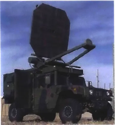
GHz to detect surrounding traffic. The Active Denial System (ADS) is a military
application which uses a high-power beam at 95 GHz for non-lethal crowd control and
perimeter security; it is depicted in Figure 1-5. If the ADS is pointed at a human, the directed energy at about 95 GHz heats up water molecules that are present in skin and creates a near-instantaneous sensation of burning without causing any physical harm or injury to the subject. The subject will retreat from the area of directed energy, relieving oneself of the burning sensation. This is effective in creating an area of
denied
access, where people are unable to enter. It may also be used in riot control todisperse a crowd without causing physical harm. Unlike the rubber bullets or pepper spray that are used in these situations today, the ADS causes no physical harm to the subject. In its current iteration, the ADS system is large and cumbersome, requiring gyrotrons to power the high-energy beam and a large transport vehicle. In addition to being difficult to transport, it is currently incapable of covering a significant area due to power restraints of the gyrotron and the need for extremely directed energy.
This thesis focuses on the W-band, but there are a wide array of applications for higher frequencies. Communications channels, radar, and imaging at higher frequen-cies have increasing benefits in bandwidths, data rates, and resolutions. For example, there is another peak in the transmission through atmosphere at 220 GHz, which could have even larger bandwidths and data rates for communications. By focusing this thesis on the W-band, we are creating an increase in our capabilities to produce high power at high frequencies which can easily be converted to even higher frequen-cies in a future experiment. In this regard, the ability to scale the experiment to higher frequencies was kept under consideration. It is not enough to just design in the W-band, one must also think toward the future of our applications and the need for power within the Terahertz gap.
The development of Traveling Wave Tubes (TWTs) at high frequencies is signif-icant because of their uses in wireless communications, satellite transponders, and electronic warfare applications. They are small, reliable, and efficient devices that provide high power for relatively high frequencies. The history of the device will be explored in the next section. Among the available vacuum electronic devices for the terahertz frequency range, TWTs are shown to be one of the most promising based off of previous experimental results and current TWT applications. Currently, TWTs
are one of the best amplifiers available in the W-band. Experimentally, they have reached average powers up to 100 W at 94 GHz. The only other amplifiers which outperform TWTs in the W-band frequency range are gyrotron devices, but they require superconducting magnets to operate. These devices are generally large and cumbersome making them impractical for many applications. TWTs offer a cheaper and more portable alternative.
Therefore, the development of a high power TWT at 94 GHz is of immediate practical use. In addition, there is a motivation to develop a new design for TWTs which has a size that is not as limited by the wavelength of operation as the traditional TWT design. A TWT of such a design would be able to easily be scaled to higher frequencies and bridge the Terahertz gap. An experimental TWT at 94 GHz with a novel cavity design is a profound scientific advancement.
1.2
A Brief History of TWTs
In the modern day, vacuum tubes are seen as a specialty field in electrical engineering. However, in the early twentieth century, even well into the 1970s, vacuum tubes were the core of electrical engineering studies. The various types of vacuum tubes were the dominant form of creating electronic systems up until the invention of the transistor in 1947. As the transistor and solid-state electronics emerged as the power-house for everyday, low power electronic devices, vacuum tubes still remained as the dominant driver in high power microwave systems. To this day, vacuum tubes are still the driving force of high power systems, and cannot be matched in performance by solid-state devices.
1.2.1
Vacuum Tubes and Radar
The first and most generic vacuum tube, the thermionic tube, was invented in 1907. These devices were the simplest form of an electronic switch and were the drive behind the first commercial electronic devices. In its most generic form, a vacuum tube consists of a cathode and anode which emit and accelerate electrons, respectively.
Output COAXIAL --TUNING
Anode
Grid- Plate OUTPUT GAP
Resonator DRIFT DISTANCE So Cathode INPUT GAP Grid- Cathode
Resonator
FLEXILE- RESONATOR
-Filaments DIAPHRAGM GRIDS
ELECTRON
. ()Input
(a)
(b)
Figure 1-6: Early vacuum tubes diagrams of (a) a tetrode
a klystron, and (c) a cavity magnetron [571, [25].
ln'erocf/on Hole S/o --A A -- Cathode (b) En7d shield End space Hole /nteract/on space
s(of
(C)tube with resonators, (b)
When a voltage is applied, the cathode emits and turns "on" the vacuum tube.
Vacuum tubes are easily used to oscillate at certain frequencies, act as relays, or
amplify signals due to a complex interaction between the electron beam in the system
and an electromagnetic wave. An early tetrode tube is shown in Figure 1-6(a), which
is designed to amplify a certain frequency.
As World War II approached, Britain began development of the first radar system
in 1935. The first military demonstration used a BBC (British Broadcasting
Corpo-ration) transmitter in order to "see" airplanes passing near. The reflected radio signal
from the planes was easily detected. The first radar system used triode thermionic
tubes with large antenna towers. It operated at 11 MHz (but the frequency was
quickly increased to 30 MHz) and able to detect airplanes up to 100 miles away
de-spite weather conditions for low visibility [55]. These systems were installed along the
coast of the UK to detect incoming airplanes, but it was quickly apparent that range
and accuracy for detection would be a key component in developing a better radar
system. It was also apparent that the installation of such a system on an airplane
would lead to superior air defenses. These requirements led to a search for higher
frequency components with high power signals.
The klystron was developed shortly after in 1937, by Russel and Sigurd Varian at Stanford. They were developing a small tube for radar which had enough power
to detect oncoming airplanes. The klystron, a powerful tube in its own right, is also important because it directed the military radar research that was being developed prior to World War II and led to the development of countless other vacuum devices. In a klystron, the electron beam travels from the cathode through a series of cavities which oscillate at specific frequencies when the beam passes through, as shown in Figure 1-6(b). The electron beam transfers energy into the electromagnetic wave in the klystron, creating an oscillation of the cavity frequency. If the klystron is driven
by an input signal, it is possible to cause an amplifying device which creates a high
power output signal in the electromagnetic wave at the input frequency.
During World War II, Germany developed radar systems with klystrons, but the
U.K. developed radar systems which used a different device, the magnetron, that was
able to provide higher power outputs. The magnetron was developed in 1939 by John Randall and Harry Boot in the UK based on previous similar devices; it is shown in Figure 1-6(c). This is the same device which, years later, would go on to power microwave ovens. (You probably have one in your kitchen.) Electrons from the center cathode are directed circularly with a magnetic field around the cavities and to the anode. The circular motion creates bunching and resonances that develop within the cavities of the magnetron. These resonances are able to be combined, leading to a high-power device. While klystrons were able to give decent power (about 500 W) at
500 MHz, the cavity magnetron provided about 50 kW at nearly 2-5 GHz, providing
a phenomenal improvement in both power and frequency.
In a key collaboration between the U.S. and U.K. in 1940, the Tizard Mission sent one of the first magnetrons to the United States. The mission led to a key international exchange of radar technology. Once in the U.S., the MIT Radiation Laboratory and Bell Laboratories quickly optimized the magnetron output and put it into mass production as part of the war effort. The magnetron was a large component of the superior British air force in World War II, and was a large driving factor in winning the war. The success of tubes in radar systems led to the development of many known types of vacuum tubes and providing the scientific knowledge to pursue new tube designs after the war.
/2. Ii.
jV*-~JI
I
C.T.
r.
Figure 1-7: Drawings from Kompfner's notebook in 1942, when he first began work
on the helical TWT. First, the TWT concept is shown with a hollow electron beam,
traveling outside of the helix. Kompfner supposed it would be a "completely untuned
amplifier" and questioned, "Would it work?" Second, a diagram of the first TWT
experiment is depicted, which has a solid pencil beam traveling through the center of
the helix [39].
1.2.2
Invention of the TWT
While working on the magnetron and related radar technology in the U.K., Rudolf
Kompfner developed the initial idea for the Traveling Wave Tube Amplifier
(Abbre-viated TWAT or TWTA in some publications, but more commonly simply called
a TWT). Figure 1-7 shows drawings from his 1942 notebook. The design involves
sending an electron beam through a slow-wave circuit; in this case, the circuit is a
helical wire which acts as the center of a coaxial input line. The helical wire slows
down the phase and group velocity of the electromagnetic wave traveling through the
device, such that the phase velocity of the wave matches the velocity of the beam.
ELECTRON GUN FOCUSING COIL INPUT 'U MATCHING * UMBIATRON 14EUX - OUTER CONOUCTOR OUTPUT FLUORESCENT SCREEN
Figure 1-8: A diagram of the first TWT experiment from Kompfner's laboratory and
a picture of John R. Pierce holding one of the first successful TWTs [39] [55].
Energy can transfer from the beam into the wave and amplification can occur. This
device was proposed as an untuned amplifier, meaning that the device would have
a significant bandwidth in comparison to its klystron and magnetron counterparts.
A detailed drawing of the TWT is shown in Figure 1-8. A focusing magnetic coil
along with other magnets (not shown) direct the electron beam through the device,
while a matching input and output circuit couple to the electromagnetic wave that is
amplified. A detailed theory of the TWT will be provided in Chapter 2.
Near the end of World War II, Kompfner and John Pierce worked together on
developing the theory and optimizing the output power and bandwidths of a working
TWT experiment. The goal was to develop a low-noise device that could be used in
radar and communications applications. John Pierce is shown in Figure 1-8 holding
one of the first successful TWTs. The helical TWT was shown to be a highly efficient
and high bandwidth device with low noise, up to 80 % efficiency, and the capability
for an octave of bandwidth (50%) [55]. Though Kompfner invented the TWT, Pierce is credited with developing the theory which ultimately led to a successful device.
The development of other types of TWTs followed. Though the helical TWT is a high bandwidth device, it has low output powers and gain characteristics. For radar transmitting, high power and gain is often necessary. In the basic theory of a TWT, a slow-wave device must be used; this device can be anything which causes the electromagnetic wave to travel at a slow velocity (less than the speed of light) such that it can be phase-matched with the electromagnetic wave. In each device, the theory remains the same, and the phase velocity of the wave can be calculated via electromagnetic field theory. Different types of TWTs led to different ranges and design trade-offs for bandwidth, gain, and power.
Using concepts from accelerator physics, high power TWTs were developed. The folded waveguide TWT is a design which uses a meandering (or serpentine) waveg-uide structure and a beam tunnel that cuts through the wavegwaveg-uide. The wave is slowed down relative to the electron beam by traveling a longer distance through a rectangular waveguide structure that folds repeatedly across the beam tunnel axis. When the beam passes through the meandering structure, it interacts with the wave.
A cooling system on the folded-waveguide TWT allows for it to be more powerful
than the helical TWT, while maintaining a relatively high bandwidth. Similarly, in a coupled-cavity TWT, the electromagnetic wave couples through subsequent cavities along the electron beam line, in much the same way as the folded-waveguide struc-ture. The coupling from one cavity to the next slows down the phase velocity of the wave to match the electron beam. The coupled cavities allow for a high power device due to the strong resonances that occur in the circuit. However, the cavities are frequency specific, and the highest achievable powers are only obtained by limiting the bandwidth capabilities of the circuit. The coupled-cavity TWT will be discussed further in Chapter 2. The varied array of possibilities with TWTs mean that a device can easily have an optimized, gain, power, and bandwidth which best suits the needs of the application at hand.
1.2.3
More Vacuum Devices
The development of the klystron, led to an array of vacuum devices that all used very similar concepts of phase-matching between the electromagnetic wave and the electron beam. These devices can be split into slow-wave devices (like magnetrons and TWTs), where the phase velocity of the wave is less than the speed of light such that the velocity matching occurs, or fast-wave devices (gyrotrons), where the phase velocity of the electromagnetic waves travel faster than the speed of light and RF interaction occurs via the angular velocity of the electron beam. It is also worth mentioning backward-wave oscillators, which are slow-wave devices that use resonances within a circuit similar to a TWT structure. The resonances cause oscillations (instead of amplifications) with a negative group velocity wave in the structure. This leads to a high power output device with a tuned frequency.
When it comes to high power in millimeter waves, no other device can match the achievements of the gyrotron. Gyrotrons are fast-wave devices which can operate as either oscillator or amplifier circuits. In gyrotrons, an annular (or hollow) electron beam is bunched azimuthally with the electric field. Gyrotron oscillators are capable of achieving extremely high output powers (more than megawatts of power) at the highest frequencies of any vacuum device, up to 100 GHz and above. Gyrotron amplifiers are capable of producing high gain at those frequencies, as well. Gyrotrons at even higher frequencies exist, and many designs are being pursued to bring gyrotron devices into the Terahertz gap. In practical applications however, gyrotrons are often seen as cumbersome; they often require high magnetic fields (10 T) which must be achieved with a superconducting magnet and are not robust to alignment issues within the magnetic field, making them hard to transport and maintain. Though gyrotrons have many applications, gyrotron devices placed in airplanes or satellites are not a practical implementation.
1.3
Modern Day W-Band Vacuum Tubes
Many advancements in vacuum tubes have occurred since the development of the device in the 1940s and 1950s. With the advent of highly accurate computer-driven simulations and optimized designs, many devices which could not be completely de-rived and understood with direct theoretical calculations can be explored without much experimental cost. In addition, machining techniques have improved, making practical implementation in the W-band easier to achieve. As such, tubes at high-frequencies have been rapidly developed in recent years.
After extensive development in the 1960s, helical TWTs have been demonstrated to provide about 1 kW of power at 10 GHz. Helical TWTs also have large bandwidths, providing up to two octaves of bandwidth at lower frequencies [21]. Folded waveguide and coupled cavity TWTs operating in the fundamental mode were developed shortly after and shown to provide approximately 100 kW of power with 10 % bandwidth up to 10 GHz in frequency [20], [37]. Scaling to higher frequencies is difficult due to small wavelengths and proportionally small structures that are difficult to manufacture.
1.3.1
W-Band TWTs
In the W-band, vacuum tube designs must deal with smaller wavelengths than the original TWT designs. (Wavelengths in this frequency range are from 4 mm to
2.7 mm.) Small operation wavelengths lead to mechanical difficulties in experimental
implementation. At 94 GHz, the wavelength of about 3.2 mm means that components that interact with this wavelength will be much smaller in size. When dealing with a TWT, this scaling also means that the electron beam must be subsequently smaller in size and will be traveling through a small beam tunnel, too. Beam compression is incredibly difficult at small sizes, and leads to extremely large magnetic fields necessary for TWT operation. (The concept of Brillouin flow will be discussed in Chapter 2.) Due to these limitations, development of high power TWTs in the W-band is not straightforward.
circuit known as the Bill James Tube developed in 1986 at Varian. With a 20 GHz bandwidth, it achieved up to 100 W continuous (CW) power and 1 kW peak output pulsed power [34], [33]. In the 25 years since, W-band TWTs have only achieved
50-100 W average power with less than 5 GHz bandwidth.
Commercially, W-band Coupled-Cavity TWTs are available with limited output power today. Off the shelf, a W-band TWT with 50 W output power from 93 to
95 GHz can be purchased from Communications & Power Industries (CPI), a
com-pany that specializes in vacuum tube manufacturing. With a limited bandwidth, a TWT with 3 kW peak power with pulsed operation can be purchased from CPI. Wide bandwidth, helix TWTs are not commercially available in the W-band. At that frequency the necessary helix size is simply too small for operation since manufactur-ing the small helix is difficult and transmittmanufactur-ing a significant electron beam through the helix requires a large magnetic field (10 T or higher is not achievable without a superconducting magnet).
Higher power TWTs are in development at industry locations as well as research labs. Research at L-3 Communications has shown the capabilities to produce a coupled-cavity TWT with 4 GHz of bandwidth and 75 W average output power for pulsed operation (150 W peak power) at 94 GHz [43]. Most notably, a complex integral-pole-piece-ferruleless-coupled-cavity folded-waveguide circuit was capable of
100 W average power, 30 dB of gain, and 1
%
bandwidth [68]. The high average power of the device was obtained through sacrificing bandwidth in the circuit, mak-ing a strongly resonant coupled-cavity device. Recent research at the Naval Research Lab has used a 3-stage folded-waveguide TWT circuit with a 3-beam electron gun, though results are forthcoming [51].In addition, theoretical analysis of many types of structures for W-band TWTs shows the limits of fundamental structures and diverse range of ideas to circumvent those limits. These investigated structures include a micro-fabricated helical struc-ture with two electron beamlets [41], a suspended ladder strucstruc-ture [42], a wood-pile electromagnetic-bandgap waveguide [16], groove-loaded folded waveguide [27], or se-lectively metalized micro-fabricated folded waveguide [62]. A cylindrical dielectric
omniguide photonic band gap TWT was in development with a 10 % bandwidth
ex-pected [64], but achieved limited success. None of these designs have been successfully
implemented in experiment and all would require small electron beam radii with large
currents and significantly larger magnetic fields than lower frequency TWTs in order
to achieve high gain conditions.
Success has come using UV-LIGA fabrication techniques. A 50 W, 220 GHz
folded waveguide TWT was successfully built at the Naval Research Lab [36]. The
small device, with a beam tunnel of about 100 microns, uses a patented UV-LIGA
method which is susceptible to small manufacturing and alignment errors. With
the development of a manufacturing process for small components, devices at high
frequencies will see larger possible gains in the coming years. However, the sizes of
the components at these frequencies puts a very strict limit on the peak output power
that can be safely handled by the devices.
Development in TWTs has also focused on complex electron beam formation.
Sheet beams, which are elliptical, as opposed to circular, solid electron beams have
been successfully used in experiments [53] [18]. In addition, multiple-beam TWTs
have up to 8 circular beams in a single device [52]. These devices are successful,
but they often require extremely precise magnetic fields and complex beam focusing
mechanisms.
1.3.2
Other W-Band Devices
Gyrotron oscillators are capable of producing extremely high output powers in the
W-band. Fueled by ITER, 1-2 MW gyrotron tubes are in development at 170 GHz.
W-band devices are also achievable with over 1 MW of output power. These designs
often have interactions in over-sized cavities and operate in an extremely high-order
mode in order to maximize interaction with an azimuthal beam [30], [38], [46], [7].
They are phenomenal devices, but require significant magnetic fields and extremely
high voltages to operate.
Extended Interaction Klystrons and Oscillators (EIKs and EIOs) in the W-band
have produced extremely high power as well. Commercially, an EIO can be purchased
which gives up to 1 kW of power in the W-band. However, the instantaneous band-width of operation is limited, at only 250 MHz for high power devices
[58].
Larger bandwidths, up to 2 GHz are available for devices with less output power [31].Solid-state devices are also not to be ignored. With advances, Amplifier Multi-plier Chains (AMCs) are capable of producing significant power in the W-band and are extremely efficient. Though expensive, purchasing a solid state device which pro-duces 50 mW of power across 10 GHz in the W-band is reasonable [48]. AMCs have a distinct scale between power and bandwidth. Devices are available with large band-width, 20 mW over the entire entire W-band (75-110 GHz), or high power, 3 W over 4 GHz [491 [61]. Though 3 W is hardly considered high power for vacuum devices, it is a great achievement for solid-state amplifiers. AMCs can be cascaded together, but reaching high powers is often prohibitively expensive, especially as the available power in solid-state devices rapidly drops off at higher frequencies.
The TWT has been shown to be a robust and capable device for numerous applica-tions. It is seen as one of the most practical vacuum tubes for modern-day endeavors, capable of producing high power and high frequency. It is also an extremely reliable device, already used for many space applications. Though devices with better output power characteristics exist at 94 GHz, it is the goal of this thesis to develop a TWT for these reasons.
1.3.3
Overmoded TWTs
Overmoded W-band TWTs have been proposed which would allow the possibility of larger beam tunnels and the need for less magnetic field overall [9], [10], [22]. An overmoded design, meaning a design which operates in a cavity mode which is at a higher frequency than the fundamental cavity mode, is oversized for its intended frequency of operation. By operating in a higher order mode, the overmoded design offers the possibility of creating a larger device than the fundamental coupled cavity equivalent at the same frequency. An oversized device offers many benefits that can lead to higher gain and power in the TWT; these benefits will be explored in this thesis.
Sheet beam EIKs are oversized devices that have been shown to be successful at
high frequencies and the technology could be applied to TWTs. By nature, these
devices are oversized for their intended frequency of operation, though they operate
in the fundamental device mode. The elliptical beam structure takes advantage of
peaks in the electric fields of the mode in the cavity or folded waveguide [53] [44].
Though moderately successful, strong and precise magnetic fields must be used to
successfully implement these devices due to the complex electron beam.
1.4
Overview of Thesis
This thesis will develop and experimentally test a novel 94 GHz overmoded
coupled-cavity TWT. Overmoded TWTs were first explored at MIT by [10].
The design
presented in this thesis is for a 94 GHz TM
31cavity mode with lower order modes
suppressed by selective dielectric loading. With the goal of experimental validation,
the design considers the practicality, manufacturing, and experimental testing of the
overmoded TWT. As the first experimental validation of an overmoded TWT, this
experiment will further expand the use of TWTs to higher frequency ranges,
imping-ing on the terahertz gap. The experimental success of an overmoded W-band TWT
will offer the possibility of scaling to higher frequencies and expanding to other modes
for operation.
In this thesis, Chapter 2 will discuss the theory of TWT design. Chapter 3 will
cover the design of an overmoded TWT circuit and Chapter 4 will discuss low power
testing of the cavity. Chapter 5 will discuss the experimental implementation of the
overmoded TWT, including the electron gun and solenoid magnet design. Chapter
6 will discuss the electron gun beam test and overmoded TWT experiment results.
Chapter2
Theory of Traveling Wave Tubes
The equations that govern Traveling Wave Tube (TWT) amplification and operation are easily described using theory derived from Pierce, and further refined over the decades, to describe different slow-wave structure interactions. This chapter will first consider an overview of the TWT interaction. A discussion on the electron beam compression with the magnetic field considerations will follow. Finally, there will be a detailed analysis of the slow-wave structure and beam-wave interaction theory.
2.1
TWT Overview
First, consider the generic TWT circuit, as shown in Figure 2-1. In this figure, an electron gun produces a beam of a specific quality. The electron beam is solid, typically round, and it is often described as a "pencil beam." It is confined and directed by a magnetic field along the -axis of the system and travels through a TWT interaction structure, as described in the next section. An electromagnetic wave is fed into the interaction structure, which interacts with the electron beam and gains energy along the length of the structure before exiting. The structure and beam-wave interaction will be described in Section 2.3 along with interaction equations. After the interaction structure, the beam exits the confining magnetic field, expands, and is deposited on a collector. All of these components are outlined in Figure 2-1 for simplicity. The beam, shown in pink, travels through the slow wave
![Figure 1-1: The Haystack Observatory 94 GHz antenna. Two sets of simulated data show a satellite that has been imaged with (a) 2 GHz or (b) 4 GHz bandwidth [11].](https://thumb-eu.123doks.com/thumbv2/123doknet/14681696.559403/22.918.124.761.122.441/figure-haystack-observatory-antenna-simulated-satellite-imaged-bandwidth.webp)

![Figure 1-6: Early vacuum tubes diagrams of (a) a tetrode a klystron, and (c) a cavity magnetron [571, [25].](https://thumb-eu.123doks.com/thumbv2/123doknet/14681696.559403/30.918.113.769.122.368/figure-early-vacuum-diagrams-tetrode-klystron-cavity-magnetron.webp)