HAL Id: hal-01159227
https://hal.archives-ouvertes.fr/hal-01159227
Submitted on 4 Jun 2015
HAL is a multi-disciplinary open access
archive for the deposit and dissemination of
sci-entific research documents, whether they are
pub-lished or not. The documents may come from
teaching and research institutions in France or
abroad, or from public or private research centers.
L’archive ouverte pluridisciplinaire HAL, est
destinée au dépôt et à la diffusion de documents
scientifiques de niveau recherche, publiés ou non,
émanant des établissements d’enseignement et de
recherche français ou étrangers, des laboratoires
publics ou privés.
Long-term Electromagnetic Robustness of Integrated
Circuits, Challenge and Trends
Alexandre Boyer, Sonia Ben Dhia
To cite this version:
Alexandre Boyer, Sonia Ben Dhia. Long-term Electromagnetic Robustness of Integrated Circuits,
Challenge and Trends. Minapad Forum 2015, Apr 2015, Grenoble, France. 6p. �hal-01159227�
Minapad 2015, April 22 and 23th, Grenoble; France
Long-term Electromagnetic Robustness of Integrated Circuits,
Challenge and Trends
A. Boyer, S. Ben Dhia
LAAS-CNRS, Université de Toulouse ; UPS, INSA, INP, ISAE ; UT1, UTM, LAAS, Toulouse, France [email protected]
Abstract
Electromagnetic compatibility (EMC) is an essential requirement to electronic systems in which integrated circuits have a major influence. Intrinsic degradation mechanisms, which produces anticipated wear-out in deep submicron (DSM) components threat not only the reliability of circuits, but also EMC performances. The need to predict and ensure long-term EMC has become a key challenge. This paper aims at presenting the last results on the long-term EMC topic, with a special focus on DSM components. The paper clarifies the effect of device degradation mechanisms on EMC level drifts during lifetime and present some attempts to predict these evolutions.
Key words: deep submicron circuit, electromagnetic compatibility, reliability, modeling
I. Introduction
Introducing new high performance and highly integrated electronic components and commercial off-the shelf (COTS) components in automotive, avionics and aerospace applications allows system manufacturers to reduce time to market delivery and manufacturing costs but forces them to analyze closely the reliability and life time with regard to the mission profiles of their applications. This trend has triggered off an increasing demand for conclusive statements about future lifetime and function of the product at early design stage, ranging from electromagnetic compatibility effects (EMC) to thermal management issues and thermo-mechanical reliability forecasts. EMC is a major requirement to electronic systems for years, in order to ensure their
insensitivity to external electromagnetic
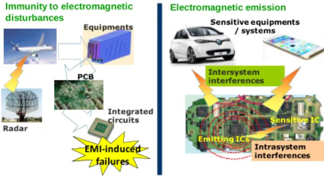
interferences (susceptibility or immunity) and their low electromagnetic radiation (emission) that could disturb neighbor equipments and systems. Ensuring both low emission and susceptibility is required to guarantee a sufficient compatibility of the different electronic systems and hence reach the functional safety level required for industrial, critical, and long duration applications. In this way, electronic integrated circuits (ICs) are at the heart of EMC concerns as they may be both perturbing (electromagnetic emission EME) and perturbed elements (electromagnetic susceptibility EMS) (Figure 1) [1].
Under market pressure toward performance and
integration increase and cost reduction,
technological evolution of CMOS technologies brings a shrink of dimensions, an introduction of new materials, a better integration rate and an enhancement of performances such as switching
speeds. However this also leads to an increase of transient current that has a direct impact on ICs parasitic emissions. Moreover the reduced supply voltages, the increased number of interfaces and mixed-signal integration tend to decrease the immunity to radio-frequency (RF) interference. EMC has become a major concern and a key differentiator in overall IC performance.
Immunity to electromagnetic disturbances Equipments PCB Radar Electromagnetic emission Intersystem interferences Intrasystem interferences Integrated circuits EMI-induced failures Emitting ICs Sensitive equipments / systems Sensitive IC
Figure 1: Central role of integrated circuits in EMC issues.
During their lifetime, ICs may be affected by failure mechanisms mainly activated by harsh environmental conditions. Intrinsic degradation mechanisms, which produces anticipated wear-out in deep submicron (DSM) components (e.g. features size 90nm and below), threat the reliability of circuits. Even if failure mechanisms may not compromise the circuit operation, IC intrinsic degradations can have a significant impact on EMC performances, as shown by recent research works. The acceleration of internal degradation mechanisms of components (passives and ICs) may lead to variations of emission and/or susceptibility levels and affect EMC margins required by the final
application. This issue is called "Long-Term EMC" and is described in Fig. 2 [2]. The need to predict EMC of ICs after several years of operating life is driven by the trend towards extended warranty. Ensuring the long-term EMC of DSM integrated circuits has become a key challenge.
This paper aims at presenting the last results on the long-term EMC topic, with a special focus on DSM components. The paper clarifies the effect of device degradation mechanisms on EME and EMS level drifts during lifetime. The paper present some attempts to predict these evolutions. Finally, the paper present on-going research axis to predict the impact of IC aging on final application EMC level.
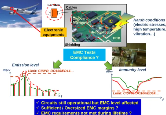
IC Electronic equipments Shielding On-board filtering Cables Ferrites PCB HF decoupling Emission level f dBµV EMC Tests Compliance ? Immunity level f dBm Harsh conditions (electric stresses, high temperature, vibration…)
Limit: CISPR, DO160/ED14…
Limit: CISPR, DO160/ED14…
Circuits still operational but EMC level affected Sufficient / Oversized EMC margins ? EMC requirements not met during lifetime ?
Figure 2: Presentation of long-term EMC issues.
II. From CMOS circuit physical degradation to EMC level drifts
1. Identification of CMOS device degradation mechanisms affecting EMC
During their lifetime, CMOS devices are affected by intrinsic failure mechanisms, such as Electro Migration (EM), Hot Carrier Injection (HCI), Negative Bias Temperature Instability (NBTI), Time Dependent Dielectric Breakdown (TDDB), mainly activated by harsh environmental conditions such as high or low temperature and electrical overstress. Among them, HCI and NBTI are the major contributors to the device electrical performance degradation in advanced CMOS technologies, since they contribute to gate oxide layer degradation. The degree of degradation of a device and, hence, its lifetime depend on the stress level and duration (Table 1). HCI and NBTI affect transistor parameters such as threshold voltage (VTH) and carrier mobility (µ), which could lead to circuit characteristic changes. Thus they have a major roles in gradual modification of IC emission and immunity levels as explained in [2], since they affect electrical behavior of internal functions such as noise margins, jitters, current consumptions, delays.
HCI NBTI Transistor type NMOS PMOS Acceleration factors High Vds, low temperature High Vgs, high temperature VTH Increase Increase µ Decrease Decrease Drain current Decrease Decrease
Other Substrate current
increase
Ioff current
increase
Table 1: Impact of oxide defects based degradation mechanisms.
2. Effect of circuit aging on electromagnetic emission
These last years, numerous experimental studies consisting in emission measurements combined with accelerated-aging conditions have been done on various type of ICs (small digital cores [3], oscillators [4], I/O buffers [5]) designed in CMOS 0.25 µm, 90 nm and 65 nm technologies. Globally, the same conclusion has been drawn from all these experiments: applying electrical or thermal stress to ICs leads to a time dependent reduction of the power integrity issues, conducted and radiated EME, whatever its technology. The technology changes only the sensitivity to stress conditions.
The studies presented in [3] clarify the link between the intrinsic degradation mechanisms accelerated by electrical stresses in a CMOS 90 nm technology and the variation of electromagnetic noise produced by I/O buffers and digital blocks. A test chip containing NMOS and PMOS transistors with various sizes and digital structures is characterized under electrical stress conditions. Figure 3 (top) shows the evolution of the threshold voltage of PMOS transistors with stress time for two different stress conditions which activate NBTI
mechanism. The threshold voltage increases
gradually with stress time according to power law. Then, these conditions are applied on a digital circuit and the power supply voltage fluctuations and conducted EME are measured according to the stress time. Figure 3 (middle) shows that the amplitude of the power supply drops due to the switching activity of the digital core decreases with stress time. The analysis of EME in frequency domain shown in figure 3 (bottom) shows that the spectral content of the conducted noise is reduced, especially in high frequency. It should emphasized that the circuit remains operational during all the stress period. The average current consumption is not affected. Only the timing characteristics such as propagation delays through the digital core increase.
0 5 10 15 20 25 30 0,1 1 10 100 1000 10000 100000 V th c h a n g e ( % ) Stress Time (s) Measurement Vstr = 1.2 V Measurement Vstr = 3.2 V Model Vstr = 1.2 V Model Vstr = 3.2 V 1548 . 0 91 . 4 t Vth = × ∆ 2627 . 0 62 . 0 t Vth= × ∆
NBTI
activation
59 mV 42 m VFigure 3: Link between NBTI (top) and power integrity (middle) and conducted emission level
(bottom) evolutions of a CMOS 90 nm digital
circuit [3].
Experimental analysis coupled with CAD simulation (see part III) helps to understand the mechanisms which lead to the general reduction of the EME. It is associated to the reduction of the amplitude and the temporal spreading of the dynamic current consumption of the IC. The acceleration of degradation mechanisms such as NBTI leads to decrease of transistor drive current and the increase of switching time, which have a direct impact on EME from electronic functions such as digital circuits or I/O buffers.
Although these results are very positive for the control of EME at IC level, the impact of aging on EME should not be overlooked. Around the IC, passive devices such as capacitors, inductors or ferrites constitute efficient filtering elements of EME. However, their characteristics drift under high temperature and high voltage conditions leading to a significant increase of conducted and radiated EME over large frequency ranges, as shown in [6]. The reduction of EME of ICs may be compensate by the filtering efficiency ensured by decoupling capacitors and HF filtering. Predicting the evolution of EME at printed circuit board (PCB) level relies on an accurate modeling of the contribution of each part: ICs and passives.
3. Effect of circuit aging on electromagnetic susceptibility
Comparing to the conclusion drawn about the impact of aging on EME, the effect of aging on EMS is less straightforward. Numerous studies have been leaded these last years to clarify the impact of aging on DSM circuit susceptibility to electromagnetic interferences. Several types of functions have been tested such as digital circuits [7], I/O buffers [5], voltage regulator, bandgap, operational amplifiers [8] and phase-locked loop [9], designed in CMOS 0.25 µm, 90 nm, 65 nm. Both positive and negative variations of the susceptibility levels have been measured after aging accelerated by electrical or thermal stresses, depending on the nature and the design of the tested functions.
The following example is proposed to illustrate the potential effect of aging on EMS of ICs, and the necessary analysis to identify the source of EMS drift [10]. A low dropout (LDO) voltage regulator designed in CMOS 90 nm technology is electrically stressed by applying high bias voltage on its power supply. This function is sensitive to electromagnetic disturbance applied on its power supply, which produces DC offset on its output. Its susceptibility to electromagnetic disturbances applied on its power supply is characterized according to stress time. Figure 4 presents the evolution of EMS level after several stress period T, where T is equal to 24 hours. Although the regulator is still functional in nominal conditions, the susceptibility level is gradually reduced over a large frequency range. In other words, this result means that the regulator operation fails for a smaller amount of electromagnetic disturbances. Experimental characterization of degradation mechanisms at transistor level and CAD simulations are necessary to understand the origin of the EMS increase. The increase of power supply voltage leads to an acceleration of NBTI some PMOS transistors of the circuit, especially the bias transistor of the internal operational amplifier (opa) of the regulator. The electrical characteristics of this transistor has a significant influence on the transconductance of the opa and on the output offset induced by the electromagnetic disturbance. Even if the characteristics of the opa are affected moderately, the regulator function is still valid in nominal conditions. However, the regulator becomes more sensitive to electromagnetic disturbances.
Gradual reduction
Figure 4: Effect of electrical stress on conducted susceptibility of a CMOS 90 nm LDO regulator [10].
III. Prediction of long-term electromagnetic compatibility of deep submicron circuits
Predictive simulation constitutes an efficient method to assess the long-term EMC of an IC, since it replaces tedious and costly experimental characterizations that mix EMC and accelerated aging tests on electronic circuits and systems. These last years, the research community which deals with EMC of ICs issues has produced a significant work about the modeling of conducted and radiated emission of ICs. Modeling standards for EMC constitute an interesting basis to propose an EME or EMS model for ICs with the integration of aging effect. Model standards propose formalisms and methodologies to build equivalent IC models dedicated to EMC prediction at PCB level. The advantages of this approach are the non-confidentiality of the IC models and the efficiency of the simulation. The following paragraphs present some first attempts to build aging-aware EME and EMS models for ICs.
1. Modeling of emission level drift
One of the main results was the proposal of the Integrated Circuit Emission Model (ICEM) standard [11], which defines a methodology to build simple and non-confidential IC model dedicated to the prediction of conducted and radiated emission. Basically, ICEM proposes to model the IC in two subblocks: the internal activity (IA) block which models the transient current produced by circuit operation, and the power distribution network (PDN) which models the filtering effect of the transient current due to IC and package.
This modeling standard constitutes an
interesting basis to propose an IC emission model which integrates the aging effect. As explained in part II.2, predicting the drift of IC emission relies on an accurate modeling of the evolution of dynamic current consumption. Changing the parameters of the IA block of the ICEM model in order to spread the IC current consumption constitutes an easy method to simulate the effect of aging. Figure 5 describes the proposed methodology to build an aging-aware ICEM model [2]. From the IC netlist and an aging model, the IC current consumption changes can be simulated and the IA block of ICEM can be updated to take into account the IC aging. The aging model may be derived from experimental characterization of degradation mechanisms and their effect on transistors in different stress conditions. Empirical relations between transistor parameters and stress condition and duration can be extracted and used to change the properties of the devices submitted to stress conditions.
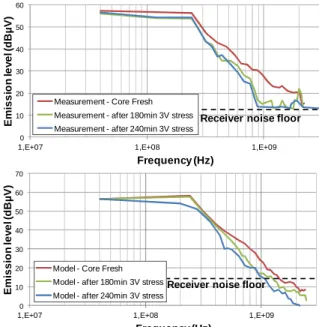
Figure 5: Aging-aware ICEM construction flow [2]. In [12], an aging-aware ICEM model of a CMOS 90 nm digital core is built. The ICEM model is representative of a fresh device. The effect of aging is inserted in the ICEM model through an empirical coefficient called "degradation ratio" which affect the parameters of the IA block according to stress condition and duration. Figure 6 presents a comparison between the measured and simulated evolution of the conducted emission spectrum when the digital core is exposed to an electrical stress. The ICEM model is able to predict with a quite good accuracy the time-dependent reduction of the conducted emission spectrum up to 1 GHz. This result demonstrates that a simple and non confidential approach based on an ICEM model ensures reasonable estimation of the evolution of the EME. 0 10 20 30 40 50 60
1,E+07 1,E+08 1,E+09
E m is s io n le v e l ( d B µ V ) Frequency (Hz)
Measurement - Core Fresh Measurement - after 180min 3V stress Measurement - after 240min 3V stress
Receiver noise floor
0 10 20 30 40 50 60 70
1,E+07 1,E+08 1,E+09
E m is s io n le v e l ( d B µ V ) Frequency (Hz)
Model - Core Fresh Model - after 180min 3V stress Model - after 240min 3V stress
Receiver noise floor
Figure 6: Measurement (top) and simulation (bottom) of the evolution of the conducted emission of a CMOS 90 nm digital core exposed to a 3 V electrical stress. [12].
2. Modeling of susceptibility level drift
The same type of approach has been followed to propose IC susceptibility models which integrate the aging effect. If the formalism described in ICEM is
reused, IC susceptibility model may be composed of two subblocks: the Power Distribution Network (PDN) which describes the coupling path of the incoming disturbances, and the Internal Behavior (IB) block which describes the nominal operation of the IC and detects the induced failures. As the PDN is not affected by aging, only the IB block will be modified. The IB block construction can be based either on experiments or on CAD simulation of the circuit netlist and modified transistor models to take into account the effect of stresses.
In [13], an aging-aware susceptibility model of a CMOS 90 nm opa is built. The opa is mounted in follower configuration. The model is representative of a fresh device. Electromagnetic disturbances coupled on the opa input lead to a voltage offset on the output, which depends on disturbance frequency and amplitude. The PDN block of the circuit has been extracted by S parameter measurements, while the IB block is formed by the circuit netlist (figure 7). The circuit is submitted to electrical stress conditions that accelerate NBTI on PMOS devices, especially M0 and M6 devices. The change of their
threshold device has been characterized
experimentally and its dependence according to stress voltage and duration is modeled by an empirical relation. V- V+ Vbias Vout Vdd Vss M1 M2 M3 M4 M5 3.3 kΩ Vbias M0 M6 M7
Figure 7: Operational amplifier structure [13]. The threshold voltage variation with stress time is then included in the transistor netlist in order to simulate the evolution of the susceptibility level according to the stress time. Figure 8 presents the measured and simulated evolution of opa output offset vs. the amplitude of a 200 MHz harmonic disturbance after various stress time. The simulation predicts correctly the increase of the offset voltage with stress time. The evolution of threshold voltage of M0 and M6 transistors leads to an increase of the slew rate of the opa and differential pair bias current but the opa remains functional in follower configuration. Nevertheless, after aging, the same amount of electromagnetic disturbance induces a larger voltage offset.
-0,6 -0,55 -0,5 -0,45 -0,4 -0,35 2 3 4 5 O ff se t (V ) Injected Power (dBm) Initial Aged_1 min Aged_10 mins Aged_100 mins Aged_1000 mins -0,6 -0,55 -0,5 -0,45 -0,4 -0,35 2 3 4 5 O ff se t (V ) Injected Power (dBm) Initial Aged_1 minute Aged_10 minutes Aged_100 minutes Aged_1000 minutes
Figure 8: Measurement (top) and simulation
(bottom) of the opa offset voltage vs. disturbance amplitude and electrical stress time [13].
IV. Towards a prediction of long-term EMC at system level
The examples presented in the previous parts have shown that IC aging leads to a gradual drift of EME or EMS levels. The amount of drifts it not straightforward since it depend on the function of the IC, the technology and the stress conditions. A major issue for manufacturers of embedded electronic systems, especially those which are intended to operate in harsh conditions, is the impact of the combined aging of all the embedded components of the electronic application. The questions that arise are: What are the risks of non compliance to EMC requirements ? Are the margins sufficient or disproportionate to compensate aging effect on EMC level ?
The development of aging-aware equivalent IC model for EMC prediction constitutes a solution to this issue. The impact of the combined aging of several embedded devices on EME and EMS may be simulated for various stress conditions. Aging-aware EMC models of circuit have to fulfill several constraints in order to reach this objective. First, a macromodeling approach should be favored in order to ensure both circuit confidentiality and a low model complexity. This last point is essential to keep reasonable simulation effort. Secondly, EMC level drifts are mainly due to degradation mechanisms activated by high temperature and electrical stress conditions. The model must reproduce the evolution of EME and EMS according to stress duration and conditions. These stress conditions should be representative of the actual operating conditions of the embedded systems. The choice of the stress conditions covered by the model has to be guided by the mission profile. Thirdly, aging process has a
statistical nature. Even if several ICs have similar EMC levels initially and are placed in identical stress conditions, a larger dispersion in EMC levels will be measured after stress. The evaluation of the risks of non compliance to EMC requirements due to aging needs statistical simulation. The stochastic approach remains underemployed for the prediction of EMC at IC level.
Figure 9 describes a simulation process dedicated to the prediction of long-term EMC of an electronic systems based on EMC-aware aging models of the embedded circuits. This process reuses the typical modeling/simulation process for EMC at PCB level. The prediction of EME or EMS level relies on models of embedded components, PCB interconnects and cables, which are subblocks of the system model. The development of these models are based on different methodologies and tools which belong to a large state-of-the-art.
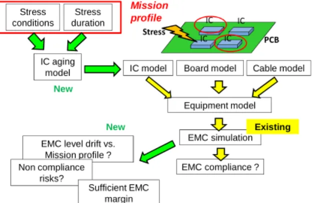
The integration of the aging requires additional information about the mission profile in order to obtain the typical stress conditions and duration. An aging model relates the stress conditions and duration to some parameters of the EMC models in order to simulate the evolution of EME or EMS levels. The results of such a simulation flow is the trend of EMC level with stress conditions and time, probability of non compliance to EMC requirements and relevance of EMC margins. The development and the validation of such a simulation flow is the one of the objective of the on-going research project "Electronic Robustness" leaded by the French institute of technology IRT Saint-Exupéry [14].
IC IC IC IC PCB
IC model Board model
Equipment model EMC simulation EMC compliance ? Stress conditions Stress duration Mission profile Stress IC aging model
EMC level drift vs. Mission profile ? Non compliance risks? Sufficient EMC margin Cable model New New Existing
Figure 9: Simulation flow for long-term EMC
prediction of an electronic embedded system.
References
[1] S. Ben Dhia, M. Ramdani, E. Sicard, "Electromagnetic Compatibility of Integrated Circuits – Techniques for Low Emission and Susceptibility", Springer, 2006.
[2] S. Ben Dhia, A. Boyer, "Long-term Electro-Magnetic Robustness of Integrated Circuits:
EMRIC research project", Microelectronic Reliability, vol. 53, pp. 1266-1272, 2013. [3] A. Boyer, S. Ben Dhia, B. Li, N. Berbel, R.
Fernandez-Garcia, "Experimental Investigations on electrical Stress Impact on Integrated Circuit EMC, vol. 56, no. 1, pp. 44-50, Feb. 2014. [4] A. Boyer, S. Ben Dhia, "Effect of aging on
power integrity of digital integrated circuits", 14th Latin American Test Workshop, 2013. [5] S. Ben Dhia, A. Boyer, B. Li, A. C. Ndoye,
"Characterization of the Electromagnetic Modeling Drifts of a Nanoscale IC after Accelerated Life Tests", Electronic Letters, vol. 46, no. 4, pp 278-279, 2010.
[6] A. Boyer, H. Huang, S. Ben Dhia, " Impact of thermal aging on emission of a buck DC-DC converter", 2014 Int. Symp. on EMC, EMC'14 Tokyo, May 2014.
[7] B. Li, A. Boyer, S. Ben Dhia, C. Lemoine, "Aging effect on immunity of a mixed signal IC", Asia-Pacific Symp. on EMC (APEMC 2010), April 2010.
[8] J. Wu, A. Boyer, J. Li, S. Ben Dhia, R. Shen, "Characterization of changes in LDO susceptibility after electrical stress", IEEE Trans EMC, vol. 55, no. 5, Oct. 2013.
[9] A. Boyer, S. Ben Dhia, B. Li, C. Lemoine, B. Vrignon, "Prediction of long-term immunity of a phase-locked loop", Journal of Electronic Test, vol. 28, no. 6, pp. 791-802, Dec. 2012. [10] J. Wu, A. Boyer, J. Li, R. Shen, S. Ben Dhia,
“Effect of Electrical Stresses on the Susceptibility of a Voltage regulator”, EMC Europe 2013, Sep 2013.
[11] IEC62433-2, "Simulation – ICEM-CE, ICEM Conducted Emission Model", International
Electrotechnical Commission, Geneva,
Switzerland, 2008.
[12] A. Boyer, S. Ben Dhia, « Effect of Aging on Power Integrity and Conducted Emission of Digital Integrated Circuits », Journal of Low Power Electronics, vol. 10, no. 1, March 2014. [13] H. Huang, A. Boyer, S. Ben Dhia, B. Vrignon,
"Prediction of Aging Impact on Electromagnetic Susceptibility of an Operational Amplifier", Asia-Pacific Symp. on EMC (APEMC 2015), May 2015.
[14] IRT Saint-Exupéry, Technological Research Center for aeronautics, space and embedded systems, http://www.irt-saintexupery.com
![Figure 3: Link between NBTI (top) and power integrity (middle) and conducted emission level (bottom) evolutions of a CMOS 90 nm digital circuit [3]](https://thumb-eu.123doks.com/thumbv2/123doknet/14395672.509071/4.892.107.422.90.553/figure-integrity-middle-conducted-emission-evolutions-digital-circuit.webp)
![Figure 7: Operational amplifier structure [13] . The threshold voltage variation with stress time is then included in the transistor netlist in order to simulate the evolution of the susceptibility level according to the stress time](https://thumb-eu.123doks.com/thumbv2/123doknet/14395672.509071/6.892.466.787.90.425/operational-amplifier-structure-threshold-variation-transistor-evolution-susceptibility.webp)