HAL Id: hal-01788148
https://hal.archives-ouvertes.fr/hal-01788148
Submitted on 17 Jul 2018
HAL is a multi-disciplinary open access
archive for the deposit and dissemination of sci-entific research documents, whether they are pub-lished or not. The documents may come from teaching and research institutions in France or abroad, or from public or private research centers.
L’archive ouverte pluridisciplinaire HAL, est destinée au dépôt et à la diffusion de documents scientifiques de niveau recherche, publiés ou non, émanant des établissements d’enseignement et de recherche français ou étrangers, des laboratoires publics ou privés.
Architecture, design and technology guidelines for
crosspoint memories
Alexandre Levisse, P. Royer, Bastien Giraud, J.P. Nöel, Mathieu Moreau,
Jean-Michel Portal
To cite this version:
Alexandre Levisse, P. Royer, Bastien Giraud, J.P. Nöel, Mathieu Moreau, et al.. Architecture,
design and technology guidelines for crosspoint memories. 2017 IEEE/ACM International Sympo-sium on Nanoscale Architectures (NANOARCH), Jul 2017, Newport, United States. pp.677 - 686, �10.1109/NANOARCH.2017.8053733�. �hal-01788148�
Architecture, Design and Technology Guidelines for
Crosspoint Memories
A.LEVISSE1,2,P.ROYER1,B.GIRAUD1,J.P.NOEL1,M.MOREAU2,J.M.PORTAL2
1Univ. Grenoble Alpes, F-38000 Grenoble, France; CEA, LETI, MINATEC Campus, F-38054 Grenoble, France
2Aix-Marseille Université, IM2NP, CNRS UMR 7334, F-13453 Marseille, France
Email: [email protected]
Abstract— While standalone Flash memories (NAND) are
facing their physical limitations, the emergence of resistive switching memories (RRAM) is seen as a solution for high density, low cost and low energy NAND replacement candidate. However, it has been shown that deeply scaled, high density RRAM architectures, such as crosspoint, suffer of voltage drop effects (IR drop) in metal lines, periphery overhead and metal line charging time due to injected current during programming operations and sneaking currents through unselected bitcells. In this work, we first propose several innovative models for IRdrop, periphery overhead and array-line charging time accounting for in-array multiple bit-write operation. Then, we introduce a new methodology for crosspoint memory design to determine IRdrop, periphery overhead and timing associated with the optimal characteristics of 1 selector-1 resistance (1S1R) device. We apply the proposed methodology to various half metal pitch memory technology nodes (from 50nm to 15nm) and to several written word sizes (from 1 to 32 bits). We show that for 1 bit programmed per array, the RRAM programming current has to be lower than 30µA and the selector leakage current lower than 10nA and that limitations increase as soon as multiple bits are written simultaneously in the same array. This, suggests massively parallel multi-bank write of a small number of bits per array, as the best solution for the RRAM memories to be competitive with NAND memories
Keywords—RRAM, crosspoint memory, crossbar memory, 1S1R NVM device, NVM
I. INTRODUCTION
The data deluge triggered by the Internet of Things (IoT) arrival in the consumer market spotlights the need for non-volatile memories (NVM) for servers/data centers (standalone NVM) and connected objects (embedded NVM). Both standalone and embedded floating gate Flash memory technologies are facing extreme process complexity and cost increase (due to multiple patterning [1], split gate [2], air gap [3], vertical stacking [4]), as well as performance reduction [5].
Facing this issue, new technologies, such as Resistive Switching Memories (RRAM) are thought as a possible replacement candidate for flash memories. Various RRAM technologies are reported and demonstrated, each based on a specific physical effect. Phase Change Memories (PCM) [6], Magnetic Random-Access Memories (MRAM) [7] and filamentary Resistive Memories (Oxide-based RRAM – OxRAM and Conductive Bridge RRAM – CBRAM) [8,9], are seen as the most popular RRAM technologies and explored as a Flash replacement candidate by both industrials and academics. The major strength of RRAM technologies compared to Flash memories is the low-cost Back-End-of-Line (BEoL) integration
[10], the write speed (down to few nano-seconds [9]) and a high scalability in the BEoL [11].
To increase the RRAM array density compared to 1 Transistor – 1 Resistance (1T1R) architecture, transistor-less architectures, such as crosspoint are reported [12,13]. To ensure operation of the crosspoint array, a BEoL Selection device must be integrated in series with the RRAM device (1S1R). BEoL selectors are widely studied in the literature [14]. However, this additional device doubling the programming voltage [9]. This ending up to a 1S1R programming voltage higher than 2.5 Volts [15]. This force the use of thicker oxide and more area consuming MOS transistors for the peripheral circuitry [16].
1S1R arrays basically enable 4F² density with minimum width and spacing metal lines. Practically, this density is however impacted by the periphery due to the high programming currents that cannot be reduced under a few tens of microamperes required to ensure a reliable writing operation [9]. This effect increases due to voltage drop effects in metal lines [17].
Few studies considering voltage drop in metal lines are reported [18-21]. However, none complete study considers the full structure of the macrocell, i.e. the crosspoint device, the array area, the array metal drop issues, the peripheral circuitry overhead and the in-array timing. Furthermore, no study considering multiple bit-write in a single array is reported. In this paper, we propose three complementary models (in-array timing, IR-drop and periphery overhead) taking into account multiple bit-write in the same array and develop a methodology allowing an extensive study of the crosspoint memories design-space.
The remainder of this paper is organized as follows; section II presents the general background of this paper and the previously published models, Section III extends the previously published models for multiple bit-write and introduce a new timing estimation model. Section IV presents an extensive study of design space of crosspoint memory array while section V discusses the results. Finally, section VI concludes the paper.
II. BACKGROUND
A. 1 Selector – 1 Resistance Bitcell Model
Selective access to RRAM requires specific devices able to drive the high programming currents. On one hand, regular
Complementary Metal-Oxide-Semiconductor (CMOS) transistors can be used for this purpose but will severely increase the bitcell area [22]. Other Front-End-of-Line (FEoL) selection devices can be used (BJTs, vertical gate-all-around transistors) at the expense of increased process cost and complexity [23] [24]. On the other hand, crosspoint transistor-less architectures have been proposed, that integrate one RRAM device at each
crossing point of word-lines and bit-lines (WL, BL) without FEoL devices in the array [12] [13]. These architectures achieve maximum bitcell density but suffer from sneaking currents through unselected bitcells (Sneakpath – SP) that quickly overtake the programming current as soon as the array size grows [25] [26]. To overcome these limitations, a BEoL selector has to be integrated in the RRAM stack. In 1S1R configuration, the SP effect is mitigated and can be efficiently compensated [25] [27] still allowing a dense 4𝐹2 bitcell area only limited by
metal pitch. However, this BEoL selector causes an increase of the programming voltages of a factor 2 at least increasing the programming voltage of the bitcells from 1 to 1.5V [6] [9] up to more than 2.5V [14] [28].
The considered 1S1R bitcell is simply modeled by two parameters introduced in Fig. 1-a. The programming current (Iprog) corresponds to the current needed to program the selected RRAM in both High (HRS) by a reset operation, and Low (LRS) Resistance States by a set operation. Usual values for Iprog are from few tens of µA up to few mA [6] [9]. The non-selected bitcells, that are polarized in half bias scheme, see a potential under the BEoL selector threshold voltage (VTH).
The unselected bitcells SP current (Isp) is determined as the leakage current of the selector at half of the RRAM programming voltage as shown in Fig. 1-b. Usual values for Isp are from pA to µA [14] [28].
Figure 1: (a) I-V curve of RRAM (blue) and 1S1R (red) bitcell. (b) Illustration of the SP in a transistor-less array architecture using 1S1R bitcells.
B. Voltage Drop Model
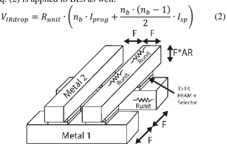
In crosspoint memory arrays, the Iprog current combined with the sum of the Isp currents results in important voltage drops that have to be considered to correctly size the RRAM-array and periphery. The line resistance equivalent to a bitcell length is defined with the half metal pitch (F), the metal aspect
ratio (AR) and the metal resistivity (σ) of the WLs/BLs (that are
supposed identical). The physical structure of a crosspoint array with detailed parameters is introduced in Fig. 2. An aspect ratio of 2 is considered for the metal lines, as suggested in the ITRS roadmap for high density memory technology nodes [29]. This, results in an increase of the resistance per bitcell as the technology is scaled, as inferred by Eq. (1), that assumes a minimum pitch bitcell.
𝑅𝑢𝑛𝑖𝑡= 𝜎 ∙ 𝐿 𝑆 = 𝜎 ∙ 2𝐹 𝐹 ∙ (𝐴𝑅 ∙ 𝐹)= 2 ∙ 𝜎 𝐴𝑅 ∙ 𝐹 (1)
The worst-case voltage drop that corresponds to the farthest bitcell being programmed is considered. The first unit resistance (Runit) sees the Iprog and Isp currents of all the bitcells in the line. For every next bitcell, the current is reduced by one-unit SP current until the last bitcell in the line is reached with only Iprog left. In the end, the total voltage drop in a WL is as shown in Eq.
(2), where 𝑛𝑏 is the number of BL connected to the selected WL.
Eq. (2) is applied to BLs as well. 𝑉𝐼𝑅𝑑𝑟𝑜𝑝= 𝑅𝑢𝑛𝑖𝑡∙ (𝑛𝑏∙ 𝐼𝑝𝑟𝑜𝑔+
𝑛𝑏∙ (𝑛𝑏− 1)
2 ∙ 𝐼𝑠𝑝) (2)
Figure 2: Physical schematic of a 2 x 2 crosspoint array with detailed physical parameters from [17].
C. Periphery Area Estimation Model
While the array area scaling is usually considered as the most critical parameter of crosspoint memories, peripheral circuitry is poorly seen in the literature as a constraint since large arrays are considered. Beyond pitch matching issues (not considered in this work) that will substantially increase the complexity of peripheral circuitry layout (due to the thicker oxide transistors needed), this section introduces a periphery area overhead model of the ratio between the multiplexer (MUX) and the decoder and the crosspoint memory array.
The area estimation methodology is described in [17]. It considers two contributions: the active area width of the transistors (that scales with the required current) and the minimum size constraints (width, length, transistor-to-transistor spacing) that has to be considered in order to provide accurate area estimation. In this work, a 150nm gate length IO transistor from a 28nm CMOS technology, reliable up to 3V, is considered. Each cell of the MUX contains two blocks, one driving WL or BL when selected, and one driving the WL or BL when not selected. The selected driver width is scaling with Iprog and Isp while the non-selected driver only scales with Isp. The decoder topology is detailed in [17] where minimum width transistors are considered.
III. MODELS
In this section, we introduce a timing estimation model based on metal lines parasitic capacitance, and extend the previous IR drop and periphery area models from [17] to include the multiple-bit programming case.
A. Timing Estimation Model
Beyond the IR-drop and overhead estimation, with the scaling of the array, the time required to charge and discharge the selected WL and BL might have a significant impact on the overall programming and access time.
The parasitic capacitance is defined as the facing lateral and vertical capacitances of crosspoint memory metal lines (while crosspoint arrays with aggressive pitch can be integrated in high BEoL levels [12], coupling capacitance with silicon substrate is not considered in this work). Two different unit capacitance contributions are considered based on the physical schematic presented Fig.2: (i) the lateral capacitance 𝐶𝑙𝑎𝑡, between the selected line and the ones running in parallel; (ii) the vertical
capacitance 𝐶𝑣𝑒𝑟, between the studied line and the ones crossing it perpendicularly.
A vertical spacing of 𝐴𝑅 ∗ 𝐹 with a typical SiO2 permittivity
(𝜀𝑟≈ 3.9) is considered. As the distance between the considered
line to the crossing lines (𝐴𝑅 ∗ 𝐹) is higher than the crossing lines pitch (F) those can be approximated by a plane. This leads to an opposing surface of 2𝐹² which considers only the fringe capacitances in the direction of the studied line.
The horizontal spacing corresponds to the pitch of the technology. This makes 𝐶𝑙𝑎𝑡 capacitance more critical. Hence, Flash NAND process commonly uses low-K insulator [30], such as air-gap (𝜀𝑟≈ 2). The opposing surface of horizontal capacitance is 2 ∗ 𝐴𝑅 ∗ 𝐹² as seen in Fig. 2. While integrating airgap represents a huge additional process cost, in the following simulations we consider typical SiO2 permittivity.
Considering all these parameters, 𝐶𝑣𝑒𝑟 and 𝐶𝑙𝑎𝑡 unit
capacitances are shown in Eq. (3) and (4), respectively. Those inferred equations only take into account fringe capacitances in the bottom metal layer direction for the vertical capacitances. An increase of 50% and 20% of the 𝐶𝑣𝑒𝑟and 𝐶𝑙𝑎𝑡 capacitances,
respectively, would still be optimistic as benchmarked with a 50nm half pitch-pitch technology.
𝐶𝑣𝑒𝑟= 𝜀𝑣𝑒𝑟∙ 𝜀0∙ 2𝐹 ∙ 𝐹 𝐴𝑅 ∙ 𝐹 = 𝜀𝑣𝑒𝑟∙ 𝜀0∙ 2𝐹 𝐴𝑅 (3) 𝐶𝑙𝑎𝑡= 𝜀𝑙𝑎𝑡∙ 𝜀0∙ 2𝐹 ∙ 𝐴𝑅 ∙ 𝐹 𝐹 = 𝜀𝑙𝑎𝑡∙ 𝜀0∙ 2𝐹 ∙ 𝐴𝑅 (4)
Once the equivalent capacitance is calculated, the worst-case bitcell is considered, that is the one laying in the last BL and WL from the MUX. Thus, the delay is calculated for a line length corresponding to the considered array parameters.
Figure 3: Two major capacitance contributions are considered, the vertical capacitance and the lateral capacitance. The equivalent schematic diagram is a ladder RC network.
The considered RC network, presented Fig. 3, is a Ladder
RC network. To simplify the calculation, an Elmore delay [31]
is considered, that approximates the time constant of 𝑛 RC units (Eq. (5)).
𝜏𝑅𝐶,𝑛=𝑛
2
2 ∙ 𝑅 ∙ 𝐶
(5) Then, the array delay is determined for 95% of the full charging time, i.e. 3 ∗ 𝜏𝑅𝐶,𝑛. The sum of charge and discharge
times of the line is considered for the last bitcell of the line and the column. Runit, and the sum of 𝐶𝑣𝑒𝑟and 𝐶𝑙𝑎𝑡 capacitances are
injected in Eq. (5) to determine the time constant.
It is interesting to note that in the considered model, the metal resistivity is proportional to 1/𝐹 while the capacitance is
proportional to 𝐹. This results in a timing estimation that is independent of the half pitch physical dimension.
B. Multiple-Bit In-Array Voltage Drop Model
When writing multiple bits, in addition to the SP current, the WL MUX has to provide Iprog times the number of bitcells that are written. These bitcells are spread along the WL. Each accessed bitcell is distributed every 𝑛𝑏/𝑛𝑝, where 𝑛𝑝 is the number of programmed bitcells and 𝑛𝑏 is the total number of bitcells in the WL, i.e., number of BLs. The BL MUX drives a single bitcell but 𝑛𝑝 BL MUX are activated simultaneously. Fig.
4-a presents an example of 2 bit-write in a 4WL-8BL array. Each red dot corresponds to selected WLs, BLs and bitcells, while each orange dot corresponds to non-selected WLs, BLs and bitcells, biased to half of the programming voltage.
The first Runit of the WL sees a total current of 𝑛𝑝∙ 𝐼𝑝𝑟𝑜𝑔+
(𝑛𝑏− 𝑛𝑝) ∙ 𝐼𝑠𝑝 corresponding to 𝑛𝑝 bitcells being programmed plus the SP currents on all the bitcells in the WL (𝑛𝑏− 𝑛𝑝). The
total current is reduced by 𝐼𝑠𝑝 every non-selected bitcell and by 𝐼𝑝𝑟𝑜𝑔every programmed bitcell (𝑛𝑏/𝑛𝑝). Eq. (6) shows the total IR drop in the selected WL. The voltage drops in both WL and BL are then added. IR drop in the WL is based on Eq. (6) while the one in the BL is based on Eq. (2). Eq. (7) shows the worst case total voltage drop when programming 𝑛𝑝 bits in a 𝑛𝑤WL and 𝑛𝑏 BL crosspoint memory array.
C. Multiple-Bit Periphery Area Estimation Model
The periphery area model has been extended to consider multiple bit writing. In particular, the sizes of the MUX are changed according to the required drives, as foreseen in Fig. 4-a. TP transistors in the BL side still only require to drive 1xIsp as only 1 active WL crosses each unselected BL.
Figure 4: (a) Organization of the decoders, MUX and array, with driving requirement for each WL and BL. (b) Schematic diagram of the proposed optimized MUX. DA0-n signals are generated by WL
and BL decoders from [17]. Unselected lines are connected to the half bias circuit through TP (orange), while selected lines are connected to the Write (WrA) and Sense (SA) Amplifiers through the transfer gates (red).
𝑛𝑏∶ n. of bit-lines (BL) 𝑛𝑤∶ n. of word-lines (WL) 𝑛𝑝∶ n. of bits programmed 𝐼𝑠𝑝∶ sneak-path current 𝐼𝑝𝑟𝑜𝑔∶ programming current 𝑉𝐼𝑅𝑑𝑟𝑜𝑝𝑊𝐿 = 𝑅𝑢𝑛𝑖𝑡∙ (𝑛𝑏∙ (𝑛𝑝+ 1) 2 ∙ 𝐼𝑝𝑟𝑜𝑔+ (𝑛𝑏− 𝑛𝑝) ∙ ((𝑛𝑏− 𝑛𝑝) + 1) 2 ∙ 𝐼𝑠𝑝) (6) 𝑉𝐼𝑅𝑑𝑟𝑜𝑝 𝑅𝑢𝑛𝑖𝑡 = (𝑛𝑏∙ (𝑛𝑝+ 1) 2 + 𝑛𝑤) ∙ 𝐼𝑝𝑟𝑜𝑔+ ( (𝑛𝑏− 𝑛𝑝) ∙ (𝑛𝑏− 𝑛𝑝+ 1) 2 + 𝑛𝑤∙ (𝑛𝑤− 1) 2 ) ∙ 𝐼𝑠𝑝 (7)
On the other hand, WL side TP transistors has to drive as many Isp as active BLs, that is, the amount of programmed bits. TG transistors driving the WLs additionally need to drive as many Iprog as written bits, while on the BL side TG transistors size remains unchanged.
The periphery area estimation model takes as an input the MUX proposed in Fig. 4-b. This MUX is more compact than the one previously published in [17]. When unaccessed, the array is disconnected from the writing circuitry and biased to
GND when 𝐸𝑁_𝑊𝑅 signal is low. When accessed (𝐸𝑁𝑊𝑅=
′1′), the Half-Bias generator (repectively the Write or Sense Amplifiers – WrA and SA) is connected to TP gate (resp. TG). TP and TG are controlled by the DA0-n signals generated by the
dynamic decoder proposed in [17]. When TG is activated, TG is turned off. TP contains only a p-type transistor because the driven voltages are higher than its threshold voltage (half of the programming voltage). TG is made of p-type + n-type MOS transistors in parallel because the selected WL or BL has to be driven to a low or high voltage without voltage loss through the MOS transistors.
IV. DESIGN SPACE EXPLORATION METHODOLOGY
In this section, we explore the design space of crosspoint memories. We introduce a design methodology that we first apply to a 1-layer crosspoint memory with 1 bit-write per array.
For filamentary-based RRAM technologies (OxRAM,
CBRAM), the assumption is taken that electro-forming step was achieved with a Iprog current. While this step is performed once in the lifetime of the device [9] MUX transistors reliability is assumed not critical and this step is considered as already achieved. During each programming operation (set or reset), programming conditions (current and voltage control, variability compensation, SP compensation) are controlled from the WrA. WLs and BLs MUX transistors have to sustain huge voltage differences across their terminals, forbidding cascode strategy. Such voltages make impossible the use of thin gate oxide transistors from sub-30nm CMOS nodes [16]. Thereby, thicker oxide 150nm gate length MOS IO transistors from a 28nm CMOS technology node are considered. Assuming a 3V CMOS operating voltage and a 2.5V 1S1R programming voltage, an IRdop of 0.5V is considered as the maximum in the following.
Figure 5: Maximum possible array size and area versus selector leakage per 1S1R and RRAM programming current. The array size is limited by the leakage and the programming current.
First, we calculate the maximum possible array size based on the IR drop model presented in section II-b and III-b. For each Isp/Iprog couple, we determine the maximum possible array size for a given set of technology parameters taken from [29]. The maximum array size is calculated by increasing progressively the array size until the IR drop reaches the 0.5V criterion introduced previously. Square arrays are considered in order to provide equalized IRdrop between the selected WL and BL. It also provides an identical sizing between WLs and BLs MUXs.
In the following, a copper metal half pitch of 25nm with a conductivity (σ25nm) of 6.8µΩ.cm-1 at 300°K and anAR) of 2 are
considered. Contacts and vias resistivity between the access transistors and the array are not considered.
Fig. 5 shows the array size (WL and BL amount) and area (µm²) versus Iprog and Isp currents. The array area is 4F²*WL*BL. Logically, the lower Iprog and Isp, the lower the effects of the IR drop, i.e., the bigger the array can be. Two main array size limitation zones are identified: the selector limiting zone and the RRAM limiting zone. While the Isp are summed along the selected WL and BL, only one Iprog is required as only one bitcell per array is programmed in this section. Thus, Isp has a higher impact in the limitation of the array size. The maximum design-able array size is directly limited by the 1S1R device specifications. As an example, a couple Iprog=40µA and Isp=10nA per device gives a 2048 WLs and BLs array.
Once the array size is determined, the total SP current consumed on the unselected WLs and BLs can be calculated. Thus, using the periphery estimation model presented in sections II-c and III-c, we calculate the MUX and decoder area of the peripheral circuitry. The MUX area is calculated using the schematic presented Fig. 4-a. In the proposed MUX, for 1 bit-write in the array (p=1 in Fig. 4-c), the p-type transistor (TP) drives Isp current while the n-type + p-type transmission gate (TG) drives Iprog + m*Isp (where m is the number of WL and BL of the considered array). The transistors width is thus calculated depending on the current consumed by the array. The total MUX area is the sum of the WL and BL MUXs. The decoder is calculated using the same methodology than the MUX. Fig. 6 presents the area of TG (blue) and TP (red). It appears that the TP transistor impact on the MUX area is negligible in regards with TG area. TG area scales with both Iprog and Isp. In this section, the dynamic decoder area is not detailed, but will be taken into account in the area overhead estimation. For high Iprog and Isp, the TP area is negligible in regards with the TG area.
Once the peripheral circuitry (MUX and decoders) and the array areas are determined, the area overhead of the periphery w.r.t. the array is calculated by dividing the periphery area by the array area. Fig 7 presents the area overhead versus Isp and Iprog current. The previous example, Iprog=40µA and Isp=10nA per device giving a 2048 WLs and BLs array, has a resulting area overhead of 45%.
With these data, it is possible to determine the requirements of a RRAM and BEoL selector devices for a specific application. As an example, in order to be competitive with Flash NAND memories, the area overhead must be lower than 20%. Thus, considering that constraint, Iprog must be lower than 30µA and Isp lower than 10nA. The resulting array size is bigger than 2500 WL and BL. As a reference, in Fig. 7, the red zone shows how a
20% area overhead limit, reduce the field of possible device specifications for the RRAM and the BEoL selector.
Figure 6: Detailed area of the TP transistor (red) and TG tranmission gate (blue) constituting the line and columns MUX, versus selector leakage per 1S1R and RRAM programming current. For high programming current and selector leakage, TP area is negligible compared to TG area.
Figure 7: area overhead of crosspoint array versus selector leakage and RRAM programming current for F=25nm.
Two 1S1R specific limitations are also presented in Fig. 7. The first one is the non-volatile minimum Iprog (Min NV Iprog). Depending on the RRAM technologies, it has been shown that a too low Iprog will result in volatile behavior or increased variability of the resistive state [32]. Thereby, this limitation gives a lower bound in the Iprog. The second limitation comes from the selector Isp that may be difficult to achieve below tens of pA.
With the increase of the array size, as introduced in section III-a, the array WL and BL charging time may become a limiting parameter. Fig. 8 presents the charging time of a crosspoint array line versus the technology node and the number of WLs and BLs. For deeply scaled half metal pitch, copper lines resistivity increases from 6.8µΩ.cm-1 (50nm) to
8.5µΩ.cm-1 (15nm) [29] [33].
Considering that, the lines charging time should not take more than 10% of the total programming pulse that can be as short as 10ns still ensuring a reliable RRAM operation [9], array size is limited by the timing. At F=25nm, 1ns charging time is achieved for a 3100 WL and BL array. In Fig 7, this maximum array size limitation is shown as a blue zone.
In this section, we explored the design space of crosspoint memories using the IR drop, the periphery area overhead and the in-array line charging time. In order to detail the methodology, we took as an example an F=25nm copper interconnect 1-layer crosspoint memory in which only one bit is written at a time.
We showed that IR drop limits the maximum possible array size whereas reduction of periphery overhead would tend to design the biggest array possible. We also demonstrate that the lower the Iprog and Isp are, the bigger arrays can be designed for an equivalent area overhead. These parameters are however physically limited and thus arbitrary large arrays cannot be achieved. Moreover, large arrays would severely impact the time required to charge and discharge the lines.
Figure 8: Charging time and discharge of a crosspoint array versus the array size and the metal half pitch F. Increase of the metal resistivity with the scaling is taken into account.
V. DISCUSSION
The proposed design methodology can be applied to any technology node used to implement a crosspoint memory array. However, when scaled, metal line resistivity and periphery overhead becomes a strong limitation. The extension to multiple-layer crosspoint memory will not impact the density due to a peripheral circuitry that will be multiplied as much as the amount of stacked crosspoint layers.
This study shows that Isp has a major impact, however, regarding the literature, arrays sizes are commonly small (576*2048 in [13] and 2048*4096 in [12]). Thus, from the point of view of the IRdrop, designing a selector providing less than 1nA SP current is not critical while the programming current cannot be reduced under few tens of micro-ampere without reliability reduction [32].
Due to huge area overhead, crosspoint bit density is lower than Flash NAND memory even though the bitcell area is the same (4F²). This gap increases as more bits are written in parallel. Fig. 9 shows the bit density of a crosspoint memory using Iprog=30µA and Isp=10nA versus the metal half pitch (from 50nm down to 15nm) for different word-length written in a single array (1bit to 32bits), and compared to other memory technologies (Flash NAND and DRAM). The presented bit densities are determined using the methodology presented in section IV and the multiple-bit write IR drop and periphery estimation models presented in section III-b and III-c. It appears that as the programmed word grows, the density quickly decreases.
While 1 bit-write enable bit densities (47Gb/cm² at F=15nm) almost competitive with planar Flash NAND densities (76Gb/cm² for F=16nm [30], 56Gb/cm² for F=19nm [34] and 28Gb/cm² for F=32nm [35]), 16 and 32 bit-write per array strongly reduce the bit density (less than 5Gb/cm² for 16 bit-write at F=15nm) lower than DRAM density (9.4Gb/cm² for F=20nm [36] and 3.8Gb/cm² for F=37nm [37]). This result
highlights the need for write a small number of bits per array in order to maximize the density.
VI. CONCLUSION
In this work, we first present 3 innovative models (IR drop, periphery overhead and timing estimation) accounting for multiple bit-write in crosspoint memory arrays. We then introduce a design methodology for crosspoint memory arrays based on the proposed models. This methodology consists in, first, calculating the maximum array size taking in account the IRdrop effects in the metal lines and then, using the array size in order to determine both the area and the overhead of the periphery. Finally, the optimal IPROG, ISP, array size and physical
BEoL specification can be determined considering the physical specifications of the 1S1R device and the in-array timing constraint. Finally, we apply this methodology to several application cases (1 to 32 simultaneous bit-write per array) and various technology nodes (from 15 to 50nm half metal pitch). We show that the area overhead and IRdrop strongly limits the crosspoint memory density (47Gb/cm² in 15nm for 1 bit-write) making it not yet competitive with flash NAND and even with DRAM for more than 16 bit-write per array. Reducing the written word length by spreading it in parallel in several banks appears as an effective way to provide competitive bit density for crosspoint memories.
VII. REFERENCES
[1] F. G. Pikus et al., "Advanced multi-patterning and hybrid lithography techniques,"
ASP-DAC, 2016.
[2] N. Do, "Scaling of split-gate flash memory and its adoption in modern embedded non-volatile applications," ICICDT, 2016.
[3] J. Seo et al., "Highly reliable M1X MLC NAND flash memory cell with novel active air-gap and p+ poly process integration technologies," IEDM, 2013.
[4] K.-T. Park et al., "Three-Dimensional 128 Gb MLC Vertical nand Flash Memory With 24-WL Stacked Layers and 50 MB/s High-Speed Programming," JSSC, 2015.
[5] L. M. Grupp et al., "The bleak future of NAND flash memory," FAST, 2012.
[6] H.-S. P. Wong et al., "Phase Change Memory," Proc. of the IEEE, 2010.
[7] D. Apalkov et al., "Magnetoresistive Random Access Memory," Proc. of the IEEE, 2016.
[8] H.-S. P. Wong et al., "Metal-Oxide RRAM," Proc. of the IEEE, 2012.
[9] E. Vianello et al., "Resistive Memories for Ultra-Low-Power embedded computing design," IEDM, 2014.
[10] F. Clermidy et al., "Resistive memories: Which applications?," DATE, 2014.
[11] X. Xu et al., "Fully CMOS compatible 3D vertical RRAM with aligned self-selective cell enabling sub-5nm scaling," IEEE Symp. on VLSI Technology, 2016.
[12] T.-y. Liu et al., "A 130.7-mm 2-Layer 32-Gb ReRAM Memory Device in 24-nm Technology," JSSC, 2014.
[13] A. Kawahara et al., "An 8 Mb Multi-Layered Cross-Point ReRAM Macro With 443 MB/s Write Throughput," JSSC, 2013.
[14] R. Aluguri et al., "Overview of Selector Devices for 3-D Stackable Cross Point RRAM Arrays," JEDS, 2016.
[15] L. Zhang et al., "Selector design considerations and requirements for 1 SIR RRAM crossbar array," IMW, 2014.
[16] X. Federspiel et al., "28nm node bulk vs FDSOI reliability comparison,"IRPS 2012.
[17] A. Levisse et al., "High Density Emerging Resistive Memories: What are the Limits ?," LASCAS, 2017.
[18] S. Kim et al., «Crossbar RRAM Arrays: Selector Device Requirements During Write Operation,» TED, 2014.
[19] J. Zhou et al., "Crossbar RRAM Arrays: Selector Device Requirements During Read Operation," TED, 2014.
[20] A. Chen, "A Comprehensive Crossbar Array Model With Solutions for Line Resistance and Nonlinear Device Characteristics," TED 2013.
[21] S. Zuloaga et al., "Scaling 2-layer RRAM cross-point array towards 10 nm node: A device-circuit co-design," ISCAS, 2015.
[22] W. C. Shen et al., "High-K metal gate contact RRAM (CRRAM) in pure 28nm CMOS logic process," IEDM, 2012.
[23] C. Wang et al., "Three-Dimensional 4F2 ReRAM With Vertical BJT Driver by CMOS Logic Compatible Process," IEDM , 2011.
[24] X. Wang et al., "Highly Compact 1T-1R Architecture (4F2 Footprint) Involving Fully CMOS Compatible Vertical GAA Nano-Pillar Transistors and Oxide-Based RRAM Cells Exhibiting Excellent NVM Properties and Ultra-Low Power Operation," IEDM , 2012.
[25] A. Levisse et al., "Capacitor based SneakPath compensation circuit for transistor-less ReRAM architectures," Nanoarch., 2016.
[26] J. Liang et al., "Cross-Point Memory Array Without Cell Selectors-Device Characteristics and Data Storage Pattern Dependencies," TED, 2010.
[27] A. Levisse et al., "SneakPath Compensation Circuit for Programming and Read Operations in RRAM-based CrossPoint Architectures," NVMTS, 2015.
[28] E. Cha et al., "Selector Devices for 3-D Cross-point ReRAM," ISCAS, 2014.
[29] "http://www.itrs2.net," [Online].
[30] M. Helmet et al., "A 128Gb MLC NAND-Flash device using 16nm planar cell,"
ISSCC, 2014.
[31] T. Lamdan, "Calculation of 'Elmore' delay for RC ladder networks," Proceedings
of the Institution of Electrical Engineers,, 2010.
[32] A. Grossi et al., "Fundamental Variability Limits of Filament-based RRAM,"
IEDM, 2016.
[33] M. H. Van der Veen et al., "Barrier/Liner Stacks for Scaling the Cu Interconnect Metallization," IITC/AMC, 2016.
[34] N. Shibata et al., "A 19nm 112.8mm2 64Gb multi-level flash memory with 400Mb/s/pin 1.8V Toggle Mode interface," ISSCC, 2012.
[35] B. T. Park et al., "32nm 3-bit 32Gb NAND Flash Memory with DPT (d̲ ouble p̲atterning t̲echnology) process for mass production," VLSIT, 2010.
[36] M. Brox et al., "An 8Gb 12Gb/s/pin GDDR5X DRAM for cost-effective high-performance applications," ISSCC, 2017.
[37] T.-K.-J. Ting et al., "An 8-channel 4.5Gb 180GB/s 18ns-row-latency RAM for the last level cache," ISSCC, 2017.
Figure 9: Extrapolated bit density in Gb/cm² for 1-layer crosspoint memories compared to planar Flash NAND and DRAM product bit densities versus the half metal pitch in nm. For bit-write in a crosspoint array, the bit density is reduced due to the higher amount of current needed in the array, i.e., increased IR drop and periphery area overhead.


![[PDF] Cours pour Apprendre le Référencement des Sites Web | Formation informatique](data:image/gif;base64,R0lGODlhAQABAIAAAP///wAAACH5BAEAAAAALAAAAAABAAEAAAICRAEAOw==)