Analysis of a Transfer Admittance Technique for Automatic Testing of
Flat Panel Displays
by
Paul R. Pilotte
Submitted to the Department of Electrical Engineering and Computer Science in partial fulfillment of the requirements for the degree of
Master of Science in Electrical Engineering and Computer Science at the
MASSACHUSETTS INSTITUTE OF TECHNOLOGY May 1992
copyright (c) Paul R. Pilotte, MCMXCII. All rights reserved.
The author hereby grants to MIT permission to reproduce and to distribute copies of this thesis document in whole or in part.
A uthor... ... Department of Electrical Engineering and Computer Science
C ertified by ... ... ... ... ....o .... ...
John L. Wyatt Professor of Electrical Engineering, MIT Thesis Supervisor
C ertified by
...
...
....4 . ... ... Henry P. Hall Seiior Staff Scientist, GenRad Thesis SupervisorA ccepted by I... ... ... %...
Campbell L. Searle Chairman, Departmental Committee on Graduate Students
MASSACHUSETTS INSTITUTE OF TECHNOLOGY
Analysis of a Transfer Admittance Technique for Automatic Testing of
Flat Panel Displays
by
Paul R. Pilotte
Submitted to the Department of Electrical Engineering and Computer Science on May 8, 1992 in partial fulfillment of the requirements for the degree of
Master of Science in Electrical Engineering and Computer Science
Abstract
A theoretical and experimental study was carried out on the use of measurements of the pixel admittances in a TFT active matrix liquid crystal display (TFT-LCD) for automatic testing of such displays. Series and parallel equivalent circuit models were used to model the admittances of individual pixels. Transmission line theory was used to model the effect of panel line resistances and shunt capacitances on the admittance measurements at various locations on the panel.
The results of experiments taken on a TFT active matrix substrate with 480 gate and 1920 drain lines showed that individual pixel admittances could be measured with a standard deviation of less than .001pF and .05nS. The measurements also showed that the series circuit pixel measurements could measure TFT on conductance with a standard deviation of less than 0. lnS. Measurements along a gate and along a drain showed that the transmission line model accurately predicted the variation in pixel admittance measurements across a panel.
The use of a transfer admittance method for panel measurements and for diagnosing defects on a TFT-LCD substrate has been shown. A test system using the transfer admittance method to quickly and automatically test and diagnose defects and characteristics of TFT-LCD panels is described.
Thesis Supervisor: John L. Wyatt
Title: Professor of Electrical Engineering, MIT Thesis Supervisor: Henry P. Hall
Acknowledgements
I would like to thank all the people at GenRad for their guidance and support over the last three years. I would especially like to thank Henry Hall with whom I have worked very closely since my first day here at GenRad. Henry's enthusiasm for his work and his 40+ years experience in measuring impedance has helped shaped me both technically and personally.
In order to make this thesis a summary of the transfer admittance test method, I have included some background material for which I was a contributor and not the principal designer. The transfer admittance test method was the invention of Henry Hall, who holds a patent for the test technique. In working with Henry since the beginning of this project, I have made contributions in all subjects described here. I was particularly responsible for the admittance measurement hardware and software implementation of the LCD test system for which I built two prototype breadboards as a proof of concept. I worked closely with Henry in developing much of the test theory. I made significant contributions in the pixel model for LCD testing, the transmission line effects, and the improvements for automatic testing. I played a smaller role in the development of the guarding theory presented at the end of chapter 2. All of the measurement data presented in this thesis was taken using the GenRad GTS-1 LCD test and measurement system with an automatic prober supplied by Tokyo Electron Limited (TEL) of Japan with whom GenRad has partnered in the development of the LCD test system.
I would also like to thank GenRad's "Looking Glass" (the company name for the LCD tester project) team with whom I have worked over the last two years in applying the theory Henry and I developed into a working test system: Pete Dolan, John Lyons, David Martin, Geoff Templeton, Tony Suto, Rick Santarpio, Sharon Albertini, Craig Dawson, Joan Schopf, Lisa Martin, Paul Porreca, and everyone else who was involved. I also thank the people at TEL for their gracious hospitality when I was in Japan acquiring data for my thesis. I especially want to thank Mick Nanbu of TEL with whom I have worked very closely over the past three years. I thank Dave Wamock, Fred Otto, and Ron Roetzer with whom I worked when I first came to GenRad and who have since started a successful company.
I want to thank Professor John Wyatt for his support and enthusiasm for my work and his suggestions for possible improvements and future work. I also thank Prof. Walter Reintjes for his work in the success of the Masters in Industry Program which enabled me to study at MIT while working at GenRad.
I would especially like to thank my family for their support in all of my education and upbringing. Thanks Mom and Dad!
Table of Contents
List of Figures. . . . .8
List of Tables . . . 11
1. Introduction . . . 12
1.1 Liquid Crystal Cell Operation. . . . 12
1.2 Liquid Crystal Display Types . . . 14
1.3 TFT Active-Matrix Topologies . . . 15
1.4 Economics of Testing AM-TFT-LCDs . . . 16
1.5 Other AM-TFT-LCD Test Methods. . . . 18
2. Transfer Admittance Test Method . . . 20
2.1 Review of Admittance and Impedance . . . 20
2.2 Summary of Transfer Admittance Test Technique . . . 23
2.3 Admittance Measurement and Calibration. . . . 26
2.4 Measurement Precision and Digital Filtering of Noise. . . . 29
2.5 Varying Measurement Test Conditions . . . 33
2.6 Effect of LCD Substrate Parameters . . . 34 2.6.1 Rprg value
2.6.2 Rcsr value 2.6.3 Rprd value
2.7 Measurement Connections Errors . . . 37
2.8 Guarding of Inactive Gate and Drain Lines . . . 40
3. Pixel Model for LCD Testing . . . 44
3.1 Equivalent Pixel Model for AM-TFT-LCD Pixels. . . . 44
3.2 Parallel Admittance Measurements . . . 46
3.3 Series Admittances to Measure TFT On Conductance. . . . 52
3.4 Measurement of TFT Off Conductance . . . 55
3.5 Characterization of LCD Operation Effects with Pixel Admittance Measurements . . . 55
3.5.1 Effect of TFT "on" Conductance on LCD Operation 3.5.2 Voltage Feedthrough Effect 3.5.3 TFT Threshold Effect 3.5.4 Pixel Leakages 3.5.5 TFT Leakages
4. Transmission Line Effects. . . . .60
4.1 Model for LCD Transmission Line Effect ... 60
4.1.1 Complete Transmission Line Model 4.1.2 Simplified Transmission Line Model 4.2 Row Measurements on a LCD panel. . ... 64
4.3 Column Measurements on a LCD Panel. . . . 67
5.
Conclusion . . . 69
Appendix 1. Glossary. . . . 71
Appendix 3.
Specifications for TFT-LCD Substrate Used for
Experimental Measurements . . . 76
Bibliography. . . . 78
List of Figures
1-1 Operation of the liquid crystal material in a LCD . . . 13
1-2 480x1920 TFT-LCD substrate with storage capacitors tied to a common Cs bus line . . . 16
1-3 Possible faults on a TFT-LCD substrate with storage capacitors tied to a Cs bus line . . . .. . . . . . . . . . . . .. . 18
2-1 Measurement of impedance or admittance. . . . 21
2-2 Two-terminal equivalent circuit models (a) Series equivalent circuit model (b) parallel equivalent circuit model. . . . 22
2-3 Ideal transfer admittance test of an LCD substrate with a guard ring . . . 22
2-4 Transfer admittance test of a TFT-LCD substrate of type "Cs tied to next gate line"... . . . .. . . . . . . . . .. . . 24
2-5 Transfer admittance test of a TFT-LCD substrate of type "no Cs capacitor". . 25 2-6 Transfer admittance test of a TFT-LCD substrate of type "Cs capacitor tied to Cs com m on line" . . . 26
2-7 Current detector block diagram . .. ... 27
2-8 Equivalent noise sources at detector input. . . . 30
2-9 Detector input noise currents as a function of Rprd . . . 31
2-10 The power magnitude response of the DFT filter with M'=23 and N'=128. The abscissa shows the DFT bin number. The Oth bin is dc while the 63rd bin is the Nyquist frequency . . . 32
2-11 Substrate connections which may affect the measurement accuracy and precision. ... 35
2-12 Three-terminal, single guard TFT-LCD substrate measurement connections . 39 2-13 Three-terminal, single guard simplified circuit diagram. . . . 39 2-14 Three-terminal, double guard TFT-LCD substrate measurement connections . 40 2-15 Circuit diagram of the LCD active matrix with some gate and drain lines left unguarded. This diagram shows the alternate current paths through the line crossing capacitances in the LCD matrix. . . . 42 3-1 Equivalent circuit model for TFT "off' and "on" measurements with a Cs common bus topology. . . . 45 3-2 Equivalent circuit model for delta admittance measurements with a Cs common bus topology. . . . 45 3-3 Simulated effect of pixel leakage conductance, Gpixel, on the measured value of AGp. Curves for measured AGp versus Gpixel are shown for three frequencies, 4kHz, 8kHz, and 12kHz. The measurement precision at 8kHz is shown for reference. . . . 48 3-4 Simulated effect of TFT on conductance, Gtft, on the measured value of AGp. Curves for measured AGp versus Gpixel are shown for three frequencies, 4kHz, 8kHz, and 12kHz. The measurement precision at 8kHz is shown for reference . . . . 4 8 3-5 ACp measurement versus dc bias voltage on a 10" panel with "Cs to next gate" topology. Measurements were made at three frequencies, 4kHz, 8kHz, and 12kH z . . . 51 3-6 AGp measurement versus dc bias voltage on a 10" panel with "Cs to next gate" topology. Measurements were made at three frequencies, 4kHz, 8kHz, and 12kH z . . . 51 3-7 ACs measurement versus dc bias voltage on a 10" panel with "Cs to next gate" topology. Measurements were made at three frequencies, 4kHz, 8kHz, and 12kH z . . . 54 3-8 AGs measurement versus dc bias voltage on a 10" panel with "Cs to next gate" topology. Measurements were made at three frequencies, 4kHz, 8kHz, and 12kH z . . . 54
3-9 Voltage waveforms for a TFT-addressed pixel. The solid line shows the voltage on the pixel pad, and the dashed line shows the voltage on the gate or scan line. Edata is the voltage placed on the drain line. . . . 57 4-1 The circuit diagram used to characterize the transmission line behavior across
gate, drain, and Cs lines . . . 61 4-2 Complex admittance diagram showing the effect on ACp and AGp from the transmission line phase shift of angle 0. Since the ideal pixel admittances are mostly capacitive, the phase shift will slightly decrease the measured ACp and will make a more pronounced increase in the measured AGp . . . 62 4-3 Circuit diagram for traditional transmission line. Equations (4.1) and (4.2) describe the voltage and current at the input to the line ... 63 4-4 Circuit diagram for calculating the transmission line effect along the gate line. 63 4-5 Circuit diagram for calculating the transmission line effect along the drain line 64 4-6 ACp measurements for row 240 on a LCD panel with Cs connected to the next gate line . . . 66 4-7 AGp measurements for row 240 on a LCD panel with Cs connected to the next gate line. A curve estimating the change in AGp across the row with the transmission line model is also shown. ... 66 4-8 ACp measurements for column 1 on a LCD panel with Cs connected to the next gate line . . . 68 4-9 AGp measurements for column 1 on a LCD panel with Cs connected to the next gate line. A curve estimating the change in AGp across the column with the transmission line model is also shown. ... 68 A2-1 Cross-sectional view of an amorphous silicon TFT with an inverted staggered structure . . . 74 A2-2 Top view of an amorphous silicon TFT with an inverted staggered structure . 75
A3-1 480x1920 TFT-LCD substrate with Cs storage capacitors connected to the next gate line. This substrate was used for all experimental measurements. . . . . 77
List of Tables
2-1 Effect of unprobed gate and drain lines for a Cs bus topology with M=480, N=1920, Cgs=0.05pF, Cgd=0.05pF, Ccsdl=0.03pF, Cs=0.5pF . . . 42 2-2 Effect of unprobed gate and drain lines for a Cs to next gate line topology with M=480, N=1920, Cgs=0.05pF, Cgd=0.05pF, Cs=0.5pF. . . . 42 2-3 Effect of unprobed gate and drain lines for a no Cs topology with M=480, N=1920, Cgs=0.05pF, Cgd=0.05pF . . . 42 3-1 Measurements of a typical pixel (G2,D4) on a 10" LCD substrate with the "Cs connected to next gate" topology. The test conditions were Ftest=8kHz, acv=3.OVpeak, TFT "off" bias=-5V, TFT "on" bias=+15V, and the unused gate and drain lines were all guarded. The mean and standard deviation were computed using 25 measurements. ... 49 3-2 Measurements of a typical pixel (G2,D4) on a 10" LCD substrate with Cs connected to next gate. The test conditions were Ftest=8kHz, acv=l.OVpeak, TFT "off' bias=-5V, TFT "on" bias=+3V. The mean and standard deviation were computed using 25 measurements. ... 53 4-1 Series R and Shunt C for the transmission line models of the three LCD topologies. . . . 62 A3-1 Specifications for 10" TFT-LCD substrate used for experiments. . . . 76 11
Chapter 1
Introduction
Active-matrix liquid crystal displays (AM-LCDs) have become an attractive solution for applications where a thin profile, light weight, and low power are requirements. AM-LCDs have been targeted for laptop displays, automotive consoles, aircraft consoles, portable televisions, and others. Their success in penetrating these niche markets will largely determine whether they can supplant the CRT in television and HDTV applications in the future.
1.1
Liquid Crystal Cell Operation
1,2AM-LCDs are the latest instance of flat panel displays made by sandwiching liquid crystal (LC) material between two glass plates. The development of room-temperature LC materials was critical to their use in displays. When LC materials are heated above their melting point, the molecules become rodlike. The class of liquid crystal materials most often used for LCDs is called cholesteric. The molecules of cholesteric liquid crystal stack in layers which have a twist and tilt giving the molecules a spiral configuration as shown in Figure 1-1. The structure of the LC molecules can be altered
C.M. Apt, "Perfecting the Picture", IEEE Spectrum, July 1985, pp. 60-63.
2 A.H. Firester, "Advances in a-Si and p-Si Active Matrices", 1990 Society for Information Display Seminar Notes, pp. M8.1-M8.18.
by applying a controlled electric field across them so the LC material serves as a light switch.
The use of LC material in a display is shown in Figure 1-1. The liquid crystal material is sandwiched between two glass plates. Chemicals are used on each plate to orient the long axes of the LC molecules in one direction. The orientation of the LC molecules on the top is designed to form a 90 degree angle with the orientation of the bottom plate. Light polarizers are deposited on each glass plate to selectively pass light which is in the same direction as the LC molecules on the respective plate. With no dc voltage applied across the plates, Figure 1-1(a), the polarized light passing through the top plate is 90 degrees shifted by the twisted liquid crystal material and passes through the second polarizer. With dc bias voltage applied, Figure 1-1(b), the LC molecules line up with the electric field and do not rotate light, and the light is blocked by the bottom plate's polarizer. The intensity of light passing through the LC cell can be controlled by varying the voltage across the two plates.
Polarizer Glass Liquid crystal director Glass Polarizer ON OFF
Figure 1-1: Operation of the liquid crystal material in a LCD. (a) With no dc bias voltage across the LC material, the polarized light is rotated 90degrees and is transmitted through the second polarizer. (b) With a sufficient dc bias voltage across the LC material, the polarized light is not rotated and is blocked by the second polarizer. (photo by Terry Scheffer, Tektronix, Inc. as it appeared in "Flat-panel Displays for Laptop Computers", Information Display, March 1989, p. 13.)
1.2
Liquid Crystal Display Types
The circuit designs for addressing the liquid pixel cells have been evolving ever since the light switching properties of LC material were first discovered. Liquid crystal material was first used in direct addressed LCDs found in watches and calculators. Later, LC material was considered for use as the light controlling element for pixels in flat panel displays. Because of the large number of pixels in a high information content display, a matrix addressing scheme was developed to replace the direct address method. Early flat panel displays used a passive addressing method with transparent conductive film to form the rows and columns. A potential between the row electrodes deposited on the top glass plate and the column electrodes on the bottom glass plate controlled the light transmission of each pixel. Due to problems in their response time, contrast ratio, and pixel cross-coupling, the passive LCDs have been replaced by active-matrix LCDs for high performance applications.
Active-matrix LCDs are expected to be the future for high information content flat panel displays. They use an active device to control the voltage at each LC cell. Unlike the passive matrix displays, the active device can maintain a voltage continuously across the LC cell, thus dramatically improving the display's contrast ratio and viewing angle. Various nonlinear devices, such a MIM diodes, nonlinear resistors and thin-film transistors (TFTs) have been proposed as the controlling pixel element3,4,5. The TFT has become the most popular choice among active-matrix designs because it affords the superior display performance. Since the transfer admittance test technique is tailored for measuring active-matrix TFT-LCDs, this thesis will consider only TFT-LCD panel types.
3 D. Pryce, "Large Area Flat Panel Displays: Diverse Technologies Vie for Dominance", Electronic
Design News, October 11, 1990, pp. 79-88.
4 S. Morozumi, "Active Matrix Displays", 1989 Society for Information Display Seminar Notes, Seminar 10, pp. 10.1-10.27.
5 W.E. Howard, "Active-Matrix Techniques for Displays", Proceedings of the Society for Information Display, 1986, pp. 313-326.
A
1.3
TFT Active-Matrix Topologies
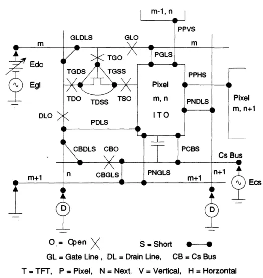
There are three dominant TFT active-matrix topologies. All topologies have the TFT gate terminal connected to the horizontal gate line, sometimes called the row or control line. The TFT drain terminal is connected to the drain line, sometimes called the column or data line. The TFT source terminal is connected to a pixel electrode. Because the TFT is a symmetrical device, sometimes the drain and source terminal names are switched. The first topology, shown in Figure 1-2, has a Cs storage capacitor connected from each pixel electrode to a common bus line. The Cs capacitor helps to maintain the charge on each pixel electrode while other rows in the display are being scanned. This is the most recent topology but is also the one with the highest defect probability because of its complexity.
The second topology is similar to the first, except it has its storage capacitors connected to the next gate line. This removes the need for the common bus line which is not present in this topology. The advantage is a simpler circuit with lower defect probabilities. However, this topology does allow the chance of crosstalk between a given pixel and the pixel to which its Cs is connected. A diagram for this topology is shown in Appendix 1.
The third topology is the oldest and least common of the three. It does not have a Cs capacitor, but instead relies on the capacitance of.the liquid crystal material deposited atop the pixel electrode to maintain the pixel voltage level while other rows are being scanned. Because the liquid crystal capacitance is a nonlinear function of voltage and has significant leakage, this topology has difficulty providing uniform pixel charge storage.
As shown in Figure 1-2, most TFT-LCD topologies use a common "guard ring" to which each gate and drain line is connected through a resistance. The "guard ring" and resistors are necessary to protect the TFTs during manufacturing. To help the liquid
crystal adhere to the glass substrate, the substrate must go through a rubbing process. This process induces static charges on the substrate and could create very large potentials between gate and drain lines which could damage the TFTs if the "guard ring" with resistors were not used.
Guard Ring Figure 1-2: 480x1920 TFr-LCD substrate with storage capacitors tied to a common Cs bus line.
1.4
Economics of Testing AM-TFT-LCDs
The development of AM-TFT-LCDs has been slowed by the difficulty in manufacturing defect-free displays. The complicated active-matrix addressing circuitry requires numerous processing steps each introducing the possibility of defects. Some of the more
A
common defects are opens in the gate or drain lines and shorts between TFT tenninals and gate or drain lines caused by pinholes in insulation layers or contaminants. Figure 1-3 is a diagram of possible faults for a TFT-LCD with storage capacitors tied to a Cs common bus6.
The extremely low yields of perfect AM-TFT-LCDs can be appreciated by considering the size and tolerance requirements. For a conventional 640x480 pixel color laptop display, 921,600 pixels must be integrated on a glass substrate measuring 10" on the diagonal. One third of these pixels are used for each of the red, green, and blue colors to make the color display. The glass substrate must be extremely flat and smooth, the deposition masks must be precisely aligned, there must be very few dust particles in the clean room, and finally there must be virtually no defects for a functional display. These production difficulties will be exacerbated in the larger HDTV displays of the future.
To lower the costs of producing good AM-TFT-LCD panels, a test and repair strategy is being considered. Testing requires an efficient technique to detect, locate, and identify panel defects. The test information could then be passed to a repair station which could use metal film deposition equipment to repair open defects and laser cutting equipment to repair short defects. The benefits of such a strategy are twofold. LCDs which have many defects could be diagnosed and disposed of at an early production stage, thus saving the expense of further production stages. Secondly, panels with a small number of defects could be economically repaired.7,8 Clearly, finding a suitable test method to diagnose pixel defects is of paramount importance in the development of AM-TFT-LCDs.
6 H.P. Hall, "Identification of Faults on TFT-LCD Substrates Using Transfer Admittance
Measurements", SID 1992 Digest, to be published.
7 R.A. Comunale, "The Color TFT-LCD: If It's Not Perfect, Fix It!", Information Display, November 1991, pp. 9-11.
8 L. Branst et al., "Laser Repair of Liquid-Crystal Displays", Information Display, September 1988, pp. 6-9.
Pixel m, n+1
" ' '"''~Ecs
D D
O = pen
X
S = Short*-GL = Gate Line, DL = Drain Line, CB - Cs Bus T = TFT, P = Pixel, N = Next, V = Vertical, H = Horzontal
Figure 1-3: Possible faults on a TFT-LCD substrate with storage capacitors tied to a Cs bus.
1.5
Other AM-TFT-LCD Test Methods
This thesis presents a test method for testing TFT-LCDs by employing transfer admittance measurements.9 10 ,11,12 The measurement theory and application to testing and characterizing these displays is explored in detail. Before beginning the discussion
9 H.P. Hall, "Method of Testing Conltrol Matrices for Flat-panel Displays", United States Patent #
5,057,775, October 15, 1991.
10 H.P. Hall and P.R. Pilotte, 'Testing TFT-LCD Substrates with a Transfer Admittance Method", paper 32.6, 1991 Society for Information Display, pp. 682-686.
11 H.P. Hall, "Identification of Faults on TFT-LCD Substrates Using Transfer Admittance Measurements", paper 21.3, 1992 Society for Information Display, to be published.
12 P.R. Pilotte, "Modeling and Characterization of TFT-LCDs Using a Transfer Admittance Test Method", paper 21.2, 1992 Society for Information Display, to be published.
of the transfer admittance test technique, references to other test methods for diagnosing TFT-LCD defects are given.
R.L. Wisnieff et al. have developed a dc test method which charges a pixel's storage capacitor and then measures the charge with a sensitive current integrating circuit. 13,14,15 F.J. Henley et al. have developed a voltage imaging method which uses the Pockel's effect to measure voltage differences at each pixel.16,17 L.H. Lin et al. have developed a method for testing the TFT array pattern by using optical spatial frequency filtering and laser holography.18
13 R.L. Wisnieff, L. Jenkins, R.J. Polastre, and R.R. Troutman, "In-Process Testing of Thin-Film Transistor Arrays", 1990 Society for Information Display, paper 11.2, pp 190-193.
14 R.R. Troutman, L. Jenkins, R.J. Polastre, and R.L. Wisnieff, "Characterization of TFT/LCD Arrays", 1991 International Display Research Conference, pp. 231-234.
15 R.R. Troutman, "Forecasting Array Yields for Large-Area TFT-LCDs", 1990 Society for Information Display, paper 11.4, pp. 197-200.
16 F.J. Henley and G. Addiego, "In-Line Functional Inspection and Repair Methodology During LCD Panel Fabrication", 1991 Society for Information Display, paper 32.7, pp. 686-688.
17 J.C. Speedy et al., "An In-Process Test System Using 'Voltage Imaging"', 1992 Society for Information Display, paper 21.4, to be published.
18 D.L. Cavan, L.H. Lin, et el., "Patterned Wafer Inspection Using Laser Holography and Spatial Frequency Filtering", Journal Vacuum Science Technology, Nov./Dec. 1988, pp. 1934-1939.
Chapter 2
Transfer Admittance Test Method
2.1
Review of Admittance and Impedance19
To understand the theory of transfer admittance testing, a brief review of the definitions and equivalent circuits for admittance and impedance is required. Since the test method measures pixel capacitances and conductances, the impedance and admittance will be defined in terms of capacitance and resistance. Small inductances in the circuit can be ignored since the impedances are high and a low frequency is used. Impedance, Z, is defined as the complex ratio of ac voltage, Eac, to ac current, Iac, through a two-terminal network, as shown in Figure 2-1. The real part of impedance is the ac resistance, R, and the imaginary part is the reactance, X. Assuming the reactance is capacitive and a radian frequency, to = 2nfrequency, Z is defined by:
Z = Rseries + jXseries = Rseries + (2.1)
J(O~series
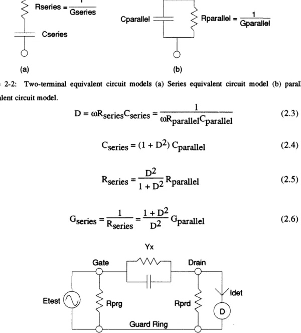
Since the impedance of elements connected in series are additive, the impedance can be modeled as an ideal resistor in series with an ideal capacitor as shown in Figure 2-2. The equivalent series parameters are denoted by the subscript 'series'.
19 "Series and Parallel Impedance Parameters and Equivalent Circuits", GenRad application note, Component Test Division.
Admittance, Y, is defined as the complex ratio of ac current to ac voltage across a two-terminal network, as shown in Figure 2-1. The real part is the ac conductance, G, and the imaginary part is the susceptance, B. Assuming the susceptance is capacitive, Y is defined by:
Y = Gparallel + jBparallel = Gparallel +
joCparallel
(2.2) Since the admittances of elements connected in parallel are additive, the admittance can be modeled as an ideal conductance in parallel with an ideal capacitance as shown in Figure 2-2. The equivalent parallel parameters are denoted by the subscript 'parallel'.lac
Eac ZorY
Figure 2-1: Measurement of impedance or admittance
Either a series or parallel equivalent circuit completely describes the impedance or admittance between two points at any given frequency. The choice of the better equivalent circuit depends on the circuit to be modeled and the frequency range of interest. In measuring pixel admittances, for example, the pixel capacitance is in parallel with some conductance and these are in series with relatively low TFT channel resistance as shown in Figure 2-3. In this case the parallel equivalent circuit is useful for finding the pixel capacitance and conductance while the series equivalent circuit is more useful for finding the TFT channel resistance. Chapter 3 will explore in detail the use of parallel and series admittance parameters to find pixel characteristics. The equations for converting between the parallel and series equivalent circuits are given in (2.3) through (2.6). The dissipation factor, D, is also defined to simplify the equations. When no
subscript is used, the parallel model is assumed for admittances and the series model is assumed for impedances.
A transfer admittance is the ratio of any current to any voltage in a circuit. The transfer admittance method described herein refers to the more specific case where the current and voltage are referenced to a common terminal, the guard ring, as shown in Figure 2-3. 1 Rseries - sre Cparallel Rparallel = 1 1 Gparallel Cseries (a) (b)
Figure 2-2: Two-terminal equivalent circuit models (a) Series equivalent circuit model (b) parallel equivalent circuit model.
1 D = (mRseriesCseries = (2.3) mORparallelCparallel Cseries = (1 + D2) Cparallel (2.4) Rseries = 1 + D2 Rparallel (2.5) 1 +D2 1 1 + D2 Gseseries = 2 Gparallel (2.6) iseries D2 Yx Gate Drain Idet
Etest i) anrn AnA4F
2.2
Summary of Transfer Admittance Test Technique
20,
21The test technique can determine pixel defects by measuring the admittances of each pixel. The main pixel admittances measured are the parasitic TFT gate-source capacitance, Cgs, and the storage capacitor, Cs. These pixel admittances are measured with a three-terminal connection using the substrate guard ring as a common point, as shown in Figure 2-4. Pixel defects are easily detected by noticing gross variations in the measured pixel admittances. For example pixels with high conductances are likely to suffer from short defects, while pixels with zero admittance are likely to suffer from line opens. Since they are directly effected by pixel defects, the pixel admittances can be efficiently used to detect, locate, and identify the many types of open and short defects on LCD panels. The high precision and accuracy measurements of pixel admittances can also be useful in characterizing other phenomena affecting LCD behavior.
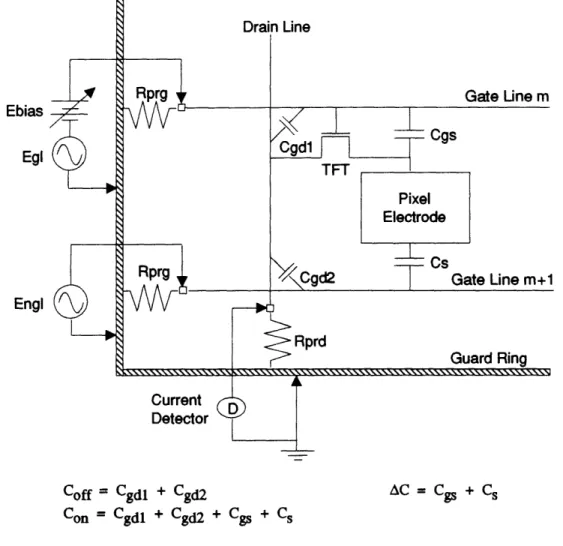
Figure 2-4 shows a pixel model for an AM-TFT-LCD pixel with a Cs storage capacitor tied to the next gate line. The sources used for ac testing and biasing the TFT are also shown. An admittance measurement is made by applying an ac test voltage to the two gate lines and measuring the resultant ac current in the drain line. The test technique requires two admittance measurements to be made, one with the TFT biased in its "on" state and one with the TFT biased in its "off" state. The "off' admittance, Goff+joCoff, is a measure of the crossover capacitance from the gate lines to the drain line. The measured "on" admittance, Gon+jo)Con, is equal to the "off' admittance plus the admittance of the pixel capacitances, Cgs and Cs. A third admittance, called a delta admittance, is calculated by taking the difference between "on" and "off' admittance measurements. This delta admittance, AG+joAC, is the most useful in detecting and
20 H.P. Hall and P.R. Pilotte, "Testing TFT-LCD Substrates with a Transfer Admittance Method", SID 1991 Digest, pp. 682-685.
21 H.P. Hall, "Method of Testing COltrol Matrices for Flat-panel Displays", United States Patent #
identifying defect pixels. In the ideal case of zero leakage across the pixel capacitors and ideal TFT switching, AG=O and AC=Cgs+Cs, for a normal pixel. These ideal assumptions of zero conductance and ideal TFT switching will be relaxed in Chapter 3 where a more detailed analysis of pixel measurements is presented.
Drain Line Rprg " Gate Line m Ebias Cgs EgR pgd T F T P ixe l Electrode Rprg ____ Cgd2 CS Gate Line m+1 E ngl
E
Z
Guard Ring Current Detector Coff = Cgdl + Cgd2 AC = Cgs + CS con = Cgdl + Cgd2 + Cgs + CSFigure 2-4: Transfer admittance test of a TFT-LCD substrate of type "Cs tied to next gate line"
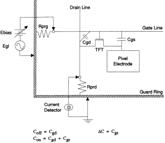
The test connections for the three types of AM-TFT-LCD panels will differ slightly. The case of the CS capacitor connected to the next gate line was just considered. The connections for a substrate with no Cs storage capacitors is shown in Figure 2-5. In this case a single ac source is used to stimulate the gate line. The delta measurement of
Ebias Icgs Egil \\ CgdOg TFT Pixel Electrode Rprd Guard Ring Current Detector Coff Cgd AC = Cgs C = Cgd + Cgs
Figure 2-5: Transfer admittance test of a TFT-LCD substrate of type "no Cs capacitor"
The connections for a substrate with the Cs capacitor connected to a common Cs line is shown in Figure 2-6. In this case the Coff measurement will be very large because of the M crossings between the Cs bus line and the drain line. The capacitance at each of these Cs bus to drain line crossings is defined as Ccsdl, and the total measured Coff capacitance will be M*Ccsdl + Cgd. In some cases the size of the Coff capacitance
forces the use of a smaller ac test voltage to keep the current detectors within their fixed range. The smaller ac test voltage will cause a proportional decrease in measurement precision. This potential problem has been solved by an "admittance subtractor" circuit which can inject a current of arbitrary magnitude and phase into the current detectors.
By appropriate setting of the "admittance subtractor", the large Coff capacitance can be
nulled. This allows the use of a larger test voltage to get improved precision in the delta admittance measurements.
Drain Line Cs Cs Common Line Ebias Egi Figure line" Coff = Cgd + M Ccsdl Con = Cgd + M Ccsd1 + Cgs + Cs
2-6: Transfer admittance test of a TFT-LCD substrate of
AC = Cgs + CS
type "Cs capacitor tied to Cs common
2.3
Admittance Measurement and Calibration
A block diagram of the current detector is shown in Figure 2-7. The small currents are amplified by a high gain transresistance operational amplifier (OpAmp) followed by subsequent moderate gain filter stages. The amplified voltage is digitized with a high-accuracy sampling A/D converter. A multi-order analog low-pass filter is used to prevent aliasing of frequencies higher than the Nyquist sampling rate, and a multi-order
high-pass filter is used to attenuate power line frequency noise at 60Hz.
Guard Ring Current
The admittance measurement utilizes a DSP-based coherent monotone testing scheme2 2. The ac voltage is measured by taking N' samples over M' cycles of the signal. If Fsamp is the converter sampling rate and Ftest is the monotone test frequency, then the fundamental requirement for coherence is shown in (2.7). If M' and N' are chosen to be relatively prime, then each sample is unique resulting in optimal information content
from the samples and a reduction of the effects of harmonics.
O Rca Etest Z or Y Rcal Rf A/D DSP Imeas -PF Converter DSP Rprd ClGl Con, Gon AC, AG
Figure 2-7: Current detector block diagram
Ftest M' (2.7)
Fsamp N'
A DFT (Discrete Fourier Transform) algorithm is used to process the A/D converter samples in calculating the admittances. An efficient DFT algorithm, the Goertzel algorithm2 3, is used to compute the M'th bin of the DFT in real time from the N' sample points. This FFT algorithm is preferable for measuring a single DFT bin because it is computationally fast and does not require extensive sine and cosine lookup tables. The real and imaginary parts of the DFT are used to compute the capacitance and conductance of the unknown. A calibration measurement of the standard resistance, Rs, is used as a reference in computing the unknown admittance. Equations (2.8) and (2.9)
22 M. Mahoney, DSP-Based Testing, Computer Press of the IEEE, 1987, pp. 17-3 1.
give the formulae for computing the unknown admittance (Gx + jBx) in terms of the standard admittance (Gs + jBs), the measurement of the unknown admittance (Gxm + jBxm), and the measurement of the standard admittance (Gsm + jBsm), the calibration
voltage (Ecal), and the measurement voltage (Emeas).
[
Bxm Bsm Gxm Bsm Gs [Gxm+ Gsm a +Bs Gsm -BxmJ Gx = 21(2.8) Emeas Gsm 1 +sm 2 Ecal G Gs Bxm -GxmBsm] + Bs Gxm + BxGBsm] Bx =21
(2.9) Emeas Gsm 1 +sm 2 Ecal GThe calibration measurements are saved for each detector circuit. When measuring an unknown, the calibration measurements for that detector are used to compute the unknown admittance. By measuring and calibrating with the same circuit, any component errors in the detector circuitry will cancel in the above calculations. This allows relaxed tolerances on the detector circuitry while maintaining high measurement accuracy. Note that the calibration and measurement voltages can be different enabling each to be selected for high measurement precision.
A method to test for saturation of the individual current detectors has been implemented in software. The test is to check the magnitude of the real and imaginary parts computed from the DFT against a predetermined upper bound. The DFT magnitude at the edge of saturation is given by the upper bound in (2.10), where Efs is the full scale voltage of the A/D converter and N' is the total number of samples. EmagUB is the Fourier transform of a sinusoid with Efs height and windowed by a boxcar of N' samples. An input voltage which saturates the A/D converter will have a voltage magnitude which is necessarily larger than EmagUB and will approach the
voltage magnitude of a windowed square wave of height Efs., shown in (2.11). The DSP software can check for A/D converter saturation by testing the voltage magnitude of any measurement against EMagUB, or some percentage of EMagUB to account for possible noise in the input voltage. If the voltage magnitude is larger than EMagLB, then the A/D converter is saturated.
Efs N'
EMagUB = 2 (2.10)
4
EMagSW = EMagUB (2.11)
2.4
Measurement Precision and Digital Filtering of Noise
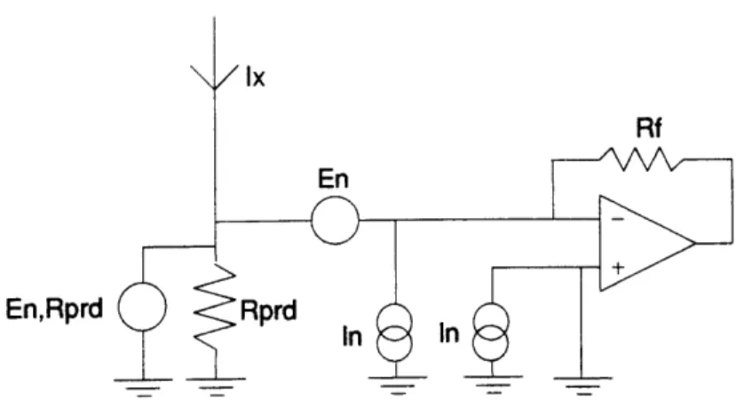
Measurements of pixel admittances must be made with sufficient precision to permit discernable differences in the measurements of good and defect pixels. Because of the very small admittance levels being measured (< .05pF in some cases), the effects of noise on measurement precision must be considered. Most of the noise will result from noise at the input to the detector. Because the detector has very high gain to measure very low currents, any noise at the detector input will likewise be amplified by the high gain.
Any noise current at the input to the first stage will be amplified and will degrade measurement precision. The dominant input noise sources are Gaussian "white" noise in the OpAmp and the Gaussian "white" thermal noise of the Rprd resistor connected across the detector input. The frequencies of interest are high enough that 1/f noise does not have a major noise contribution.
Ix
Rf En
En,Rprd Rprd In In
Figure 2-8: Equivalent noise sources at detector input
The method of modeling OpAmp noise as both current and voltage noise sources referenced at the OpAmp's inputs will be used2 4,2 5. Figure 2-8 shows the current and voltage noise sources at the detector input. In and En are defined as the total input referred OpAmp current and voltage noises. These are found by multiplying the OpAmp's current and voltage noise spectral densities (NSD), expressed in pA and nV per root Hertz, by the square root of the circuit's equivalent noise power bandwidth, (ENBW). En,Rprd is the familiar Johnson or thermal noise of the Rprd resistor as shown in (2.12), where k is the Boltzmann constant (1.38e-23 J/degK), T is temperature (degK), and BW is equal to the ENBW:
En,Rprd- 4(k)(T)(BW)(Rprd) (2.12)
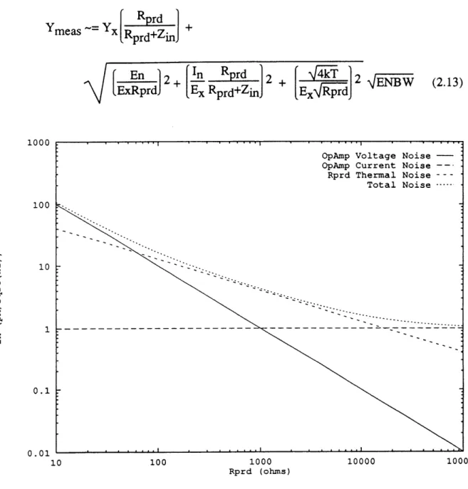
If En and In are uncorrelated, then the error terms in the admittance measurement are as shown in (2.13). The Rprd resistor, which is often integrated onto the LCD substrate for protection against static discharge, becomes a significant noise source. A graph of the total input referred noise current versus Rprd is shown in Figure 2-9. The graph shows that the thermal noise of Rprd dominates for 60ohms<Rprd<20kohms and the transresistance amplifier's current noise dominates when Rprd is larger. Because low operational amplifier voltage and current noise are opposing performance criteria in
24 H.W. Ott, Noise Reduction techniques in Electronic Systems, 1988, pp. 267-272.
25 D. Soderquist, "Minimization of Noise in Operational Amplifier Applications", Precision Monolithics Application Note, pp. 1-11, Dec. 1975.
OpAmp design, a choice of a low current or low voltage noise OpAmp may be beneficial depending on the size of Rprd.
Ymeas ~= x RRprd] +
[IEn
in Rprd 2r .T 2+ -- 2 + 2 VENBW (2.13) ExRprd ExRpdZn E d 1000 100 10 1 1 0.1 0.01 -10 100 1000 10000 100000 Rprd (ohms)Figure 2-9: Detector input noise currents as a function of Rprd.
An important function of the DFT is digital filtering of broadband noise. The DFT parameters set the equivalent noise power bandwidth (ENBW) defined above, assuming adequate low-pass filtering is used to reject noise above the Nyquist frequency. For a rectangular windowing function, the ENBW is defined in (2.14). This clearly
shows that improved measurement precision can be obtained by using a longer test time. The filter power magnitude response is shown in figure 2-10 for a 128-point DFT of 23 test cycles at 8000Hz test frequency. The graph shows that the digital filter has nulls at frequency multiples of Ftest/M', except at the signal of interest, Ftest, where the magnitude response peaks. The ENBW is the power bandwidth which equals the area under the filter's power magnitude response shown in figure 2-10. It can be shown that the rectangular window used is the optimal window for minimizing white noise error because this window has minimal ENBW2 6.
Ftest 1 M' -test time 100 U U LL~ U
I
10-1 10-2 10-3 10-4 0 10 20 30 40 Normalized Frequency 50 (2.14) 60Figure 2-10: The power magnitude response of the DFT filter with M'=23 and N'=128. The abscissa shows the DFT bin number. The 0th bin is dc while the 63rd bin is the Nyquist frequency.
Equation (2.14) can be used to estimate a lower bound for the standard deviation of the admittance measurement. An example is a typical measurement condition of
26 F.J. Harris, "On the Use of Windows for Harmonic Analysis with the Fourier Transform", Proceedings of the IEEE, Vol. 66, No. 1, January 1978, pp. 54,55.
.
---Rprd=500ohms, test time=3msecs., Ex=lVrms, and Zin<<Rprd. For an LT10282 7 low noise OpAmp, En=lnV/rootHz, In=lpA/rootHz. Figure 2-9 shows a total noise current of 6pA/rootHz. From (2.14), the ENBW is 333Hz. Using these numbers, the rms error in admittance, which is equal to the standard deviation, is Gerror=O.1nS and Cerror=.002pF.
There are other noise sources in the measurement circuit which have been neglected because they have negligible contributions to the total noise. These include the noise in the TFT itself which is dominated by the shot noise, the source's voltage noise, the thermal noise from the gate and drain line resistances which will rms add to the source's voltage noise, and electromagnetic interference noise which may couple into the detector through the gate or drain cables. The source's equivalent voltage noise sources are negligible when a very low admittance is being measured since the noise current through the test admittance will be so small. However, these source voltage noises may become important when a large off admittance is measured. For instance a panel with the Cs bus connection has a large Coff and therefore will be more susceptible to source voltage noises than other topologies.
2.5
Varying Measurement Test Conditions
The conditions of test frequency, ac test voltage, and dc bias voltage can be adjusted to optimize the measurement of various panel parameters. The test frequency can be adjusted to reduce or accentuate the transmission line behavior across the gate and drain lines of the LCD panel. Lower frequencies reduce the transmission line effect and permit more accurate measurements of the pixel capacitances. Higher frequency measurements accentuate the transmission line effect which can be used to quantify the propagation
27 Linear Technology 1990 Databook, p. 2-162. 111
delay of signals across the drain or gate lines during operation. These transmission line effect issues will be explored in more detail in Chapter 4.
The dc bias voltage can be adjusted to measure the pixel capacitances at various degrees of TFT turn on. A dc bias voltage test can be used to determine the TFT threshold voltages. The TFT threshold voltage is important because large variations in it may cause poor LCD performance.
The test voltage level can be increased to improve the measurement precision. Equation (2.13) shows that the "white" noise admittance terms can be reduced by increasing Etest. The size of Etest is somewhat limited for the Cs common LCD panel type because a large Coff capacitance results from the many crossovers between the Cs bus and each drain line. Although each crossover capacitance is small (< .03pF), there are typically 480 crossings resulting in a total measured Coff capacitance exceeding l4pF. This Coff takes up almost 98% of the A/D converter's dynamic range for typical pixel capacitances of 0.3pF. The "admittance subtractor" method, which introduces a "bucking" current of arbitrary magnitude and phase, can be used to subtract this large Coff capacitance and allow higher test voltages.
2.6
Effect of LCD Substrate Parameters
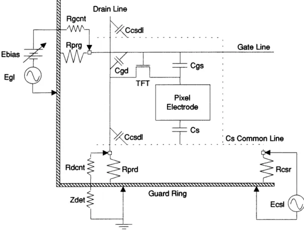
The admittance measurements will depend on the LCD substrate's design parameters and on the imperfections in the test connections. Differences in panel design and connections must therefore be considered when interpreting the measurements. This chapter will analyze the important substrate and connection effects and will present formulae for predicting the effects.
Figure 2-11 shows the various substrate parameters which may influence the admittance measurements. The values of Cgs, Cs, and Ccsdl will have a direct effect on the measured Coff and AC as was shown in Chapter 3. The effect of line resistance was
quantified in the transmission line effect discussion in Chapter 4. The values of Rprg, Rprd, and Rcsr will also influence the admittance test.
Drain Line Rgcnt csdl Rprg Gate Line Ebias gs Eg ~Cgd TFT Pixel Electrode Ccsdl CT Cs Common Line Rdcnt Rprd Rcsr Guard RingA Zdet Es csr
Figure 2-11: Substrate connections which may affect the measurement accuracy and precision.
2.6.1 Rprg value
Rprg is the resistance between the gate probe pad and the guard ring. The value of Rprg must be large enough to allow the current-limited voltage sources to drive the gate line without distortion. A large current will flow through a low Rprg and must return to the source through the guard ring. This creates voltage drops along the gate guard ring which may stimulate other gate lines.
The combination of Rprg and the gate pad contact resistance, Rgcnt, may cause a voltage divider error thus reducing both the ac and dc voltage stimulating the gate line:
-Rgent
Error from Rgcnt = Rprg + Rgnt 100% (2.14) The attenuated ac or dc voltage will result in an accuracy error in all admittance measurements. Perhaps more important than this is a variation in either Rgcnt or Rprg which will cause a relative error in measurements on different gate lines. The variation error between pixels of different gate lines must be included in the pixel measurement precision in determining the ability to detect faults.
Rprg is also necessary in guarding the gate lines when the distributed return connection is not used. This guarding effect and the potential errors caused by improper guarding will be examined in Section 2.8.
2.6.2 Rcsr value
Rcsr is the resistance between the Cs bus pad and the guard ring. The effect of Rcsr is similar to that of Rprg; its value must be large enough to allow the source to drive it and to reduce the voltage attenuation error due to the Cs bus pad contact resistance. In the case where there are multiple Cs bus pads, the Rcsr resistance is the value of the Cs bus-to-pad resistance of a single pad divided by the number of pads.
2.6.3 Rprd value
Rprd is the resistance between the drain pad and the guard ring. The Rprd value will influence three separate effects. First, there will be a current division error due to the finite input impedance of the current detector. Variations in the Rprd value or in the drain pad contact resistance, Rdcnt, or the detector input impedance, Zdet, will cause measurement errors between drain lines as shown in (2.15). The error from Zdet is eliminated by using a calibration procedure. The drain pad contact resistance error will be constant for all measurements on the same column of the display. For this reason and
because all column measurements are made with the same processor, good and bad pixels are diagnosed along a column.
Secondly, the Rprd values must be sufficiently low to guard the drain lines not being detected. An explanation of this error is given in Section 2.8. Thirdly, the Rprd will contribute to the white noise errors at the detector input. As was described in Section 2.3, Rprd causes both a thermal noise error term and a current noise error term at the input of the transresistance amplifier. Figure 2-9 showed the total input referred noise as a function of the Rprd value.
-(Rdcnt + Zdet)
Drain errors = Rprd + Rdcnt + Zdet x 100% (2.15)
2.7
Measurement Connections Errors
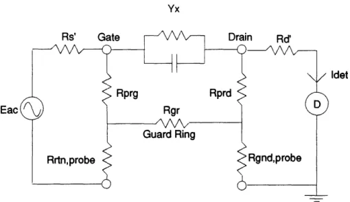
A simplification of the test connections circuit diagram was shown in Figure 2-3. The pixel admittance is measured by the ratio of detected current, Idet, to the source voltage, Etest. Here, all components, sources, and detectors are assumed to be ideal. The source has zero output impedance, the detector has zero input impedance, substrate probe connections have zero contact resistance, and the gate line, drain line, and guard ring all have zero resistance. The source return and detector ground are connected and are each tied to the guard ring. With these simplifications the measured admittance is identical to the desired pixel admittance, Yx, as shown in (2.16).
Imeas = (2.16)
~meas = Etest
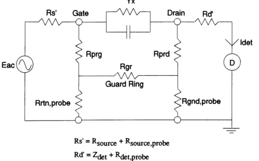
In practice the line resistance, source and detector impedances, and probe resistances must be considered. The non-ideal test connections to the substrate are shown in Figure 2-12. A A-Y transformation2 8 is used to simplify the analysis and the resulting
28 "Electric Circuits: A First Course in Circuit Analysis for Electrical Engineers", MIT electrical
circuit is shown in Figure 2-13. The grounding of the source and detector will have an important effect on measurement accuracy. The simplest grounding scheme, but one which introduces a large error term, is to connect the source return and the detector ground. This topology is called a "three-terminal, single-guard"2 9 measurement. If the error terms are small, the measured admittance can be expressed as:
Y Imeas (Yx[1 Rs' Rd' Rc
(217)
mEtest - (Rs'+Rd')Yx - Rprg Rprd YxRprgRprd(
where:
Rc -= Rrtn.probe Rgnd.probe (2.18)
Rgr
The last term is an error due to resistance in the single guard lead. Using typical numbers, Ftest=8000Hz, Rrtn.probe=3ohms, Rgnd.probe=3ohms , Zx-1=(2n8000)(l5pF), Rgr=100, Rprg=500W, Rprd=500W, the error term results in a -48% error in impedance.
The problematic guard lead error term in (2.17) can be avoided with the use of a double guarded measurement as shown in Figure 5-4. This requires a "floating" source whose return connection is isolated from the detector's ground point. The "floating" source gives a "three-terminal, double guard"3 0 measurement. Now the measured impedance has the small error terms shown in (2.19)
Ym= ~= x 1l - (Rs+Rd)Yx - R - Rd - RgrYx (2.19)
Etest -=Rprg ~Rprd
The "three-tenninal, double guard" measurement is the preferred method of testing TFT-LCD substrates with a guard ring, when the Rprg and Rprd resistors are relatively low. When Rprg and Rprd are very high, the source return must be connected to the detector
29 "Multi-terminal Impedance Measurements, or... Why Do Those New Bridges Use So Many
Connections?", GenRad application note, Component Test Division.
ground to provide a return path for the current. In this case the guard lead error term is very small. Yx Idet Rs' = Rsource + Rsource,probe Rd' = Zdet + Rdet,probe
Figure 2-12: Three-terminal, single guard TFT-LCD substrate measurement connections
Yx Idet Eac Assuming: R Fmprobe << R Tgr Rgnd,probe << Rgr Figure 2-13: Three-terminal, Rprg' ~= Rprg Rprd' Rprd Rrtn.probeRgndprobe s gr
Yx I IIdet Rprg Rprd Eac Rgr D Guard Ring Rrtn,probe Rgnd,probe
Figure 2-14: Three-terminal, double guard TFT-LCD substrate measurement connections
2.8
Guarding of Inactive Gate and Drain Lines
The accurate measurement of the pixel admittances embedded in a matrix of lines requires proper guarding of the unused lines. In this discussion the inactive lines refer to all lines other than the single gate line being stimulated and the drain lines whose currents are being detected. Every gate and drain line crossing in the matrix has some capacitance. These capacitances can provide alternate paths for the test current to flow from the source to the detector. To break these alternate current paths, guarding by connecting the unused gate lines to the source return and the unused drain lines to the detector ground can be very effective.
When the substrate being tested has a guard ring with low-valued Rprg and Rprd resistors, the matrix can be adequately guarded by probing the guard ring in several places. Probes along the gate side of the guard ring should be connected to signal return and probes on the drain sides of the guard ring should be connected to detector ground. This will maintain the preferred "three-terminal, double guard" measurement topology.
In cases where there is no guard ring or the Rpr resistors are very high, proper guarding is done by probing the unused gate and drain lines. In this case both the unused
gate probes and the unused drain probes should be connected to the source return to provide a direct path for the current from the alternate paths to return to the source. If the drain probes were grounded, the current in these probes would return through the guard ring and may cause measurement errors if they cause significant voltage drops in the guard ring.
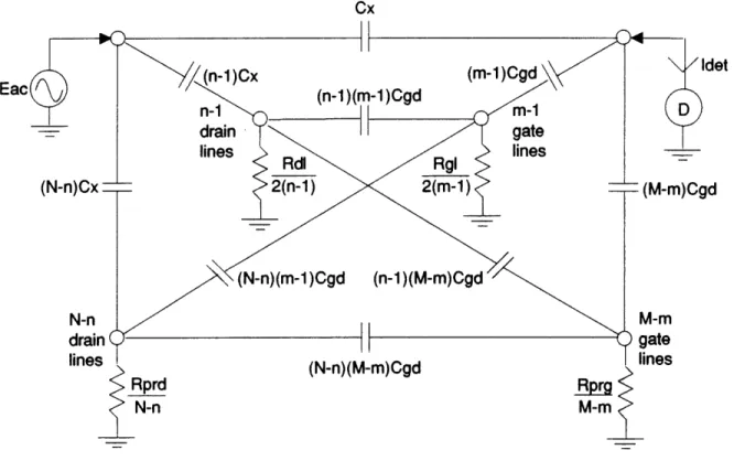
In some cases it is impractical to probe all of the gate and drain lines. Unprobed lines will be left unguarded and may cause measurement errors. Figure 2-15 shows the circuit diagram for the case where some of the gate and drain lines are left unguarded. In this diagram, N is the total number of drain lines, n is the number of probed drain lines, M is the total number of gate lines, and m is the number of probed gate lines. Cx is the capacitance between the gate line and drain line being tested and will be different for the TFT "off" and "on" measurements. In the case where a Cs storage capacitor is connected to a Cs bus or to an adjacent gate line, Cx also includes the capacitance from the extra gate or Cs bus line to the drain line being tested.
The case of infinite Rprd and Rprg is considered here because it causes the largest guarding errors and also simplifies the analysis. Since the probed gate and drain lines are connected to signal return or detector ground, their resistances are ideally zero. The effect of resistance in the gate and drain lines has little effect on the results, and therefore Rgl and Rdl will be assumed to be zero. With these assumptions, the measured capacitance will be:
(N-n) (M-m) Cgd Cx
Cm = Cx + n (M-m) Cgd + N (Cx + (m-1) Cgd) (2.20) The second term in this equation is the error in the measurement due to improper guarding. Tables 2-1 to 2-3 show the errors in Coff, Con, and ACp for different numbers of unprobed gate and drain lines for the three different LCD substrate topologies. The error tables show that it is always preferable to measure with all of the gate and drain
lines probed and guarded. The near zero ACp error with m=1 and n=1 shown in table
5-1 results from the high Cx capacitance for both on and off measurements. This example
of an unguarded measurement is not preferred because of the large errors in the Coff and Con measurements.
Cx
(n-1)Cx (m-1)Cgd Idet
Figure 2-15: Circuit diagram of the LCD active matrix with some gate and drain lines left unguarded. This diagram shows the alternate current paths through the line crossing capacitances in the LCD matrix.
m n Coff Error (pF) Con Error (pF) ACp Error (pF)
1 1 23.92 23.92 0.001
120 480 7.82 7.93 0.11
240 960 2.67 2.72 0.05
360 1440 0.59 0.60 0.01
480 1920 0.000 0.000 0.000
Table 2-1: Effect of unprobed gate and drain lines for a Cs bus topology with M=480, N=1920, Cgs=0.05pF, Cgd=0.05pF, Ccsdl=0.03pF, Cs=0.5pF.
Table 2-2: Effect of unprobed gate and drain N=1920, Cgs=0.05pF, Cgd=0.05pF, Cs=0.5pF.
lines for a Cs to next gate line topology with M=480,
Table 2-3: Effect of unprobed gate and drain lines for a no Cs topology with M=480, N=1920, Cgs=0.05pF, Cgd=0.05pF.
m n Coff Error (pF) Con Error (pF) ACp Error (pE)
1 1 21.28 23.45 2.17
120 480 0.128 0.733 0.605
240 960 0.033 0.194 0.161
360 1440 0.007 0.039 0.032
480 1920 0.000 0.000 0.000
m n Coff Error (pF) Con Error (nS) ACp Error (pF)
1 1 19.15 21.28 2.13
120 480 0.064 0.128 0.064
240 960 0.017 0.033 0.016
360 1440 0.003 0.007 0.004
Chapter 3
Pixel Model for LCD Testing
This chapter introduces an equivalent pixel model used to interpret the transfer admittance measurements. The model will show that the parallel delta admittances, ACp and AGp, and the series delta admittances, ACs and AGs, can be used to detect pixel faults and to characterize individual pixels. To a first approximation the delta admittance measurements are only effected by the components of a single pixel. This model assumes that the line resistances and shunt capacitances are small and have negligible effect on the measurements. Chapter 4 will present a transmission line model which quantify the effect of these line resistances and shunt capacitances.
Experiments made on a 10" LCD substrate will be used to show the validity of the pixel model. Refer to Appendix 1 for more information on the 10" LCD substrate used in these experiments.
3.1
Equivalent Pixel Model for AM-TFT-LCD Pixels
Figure 3-1 shows an equivalent pixel model for the AMLCD topology with Cs connected to a common Cs bus. This topology was chosen for discussion because it shows the clear advantage in measuring with parallel admittances. To isolate each pixel, the measurements of Coff, Goff, Con, and Gon should be made using a parallel equivalent circuit model. Then, the computed delta admittances, ACp and AGp, will cancel the