HAL Id: hal-02104915
https://hal.archives-ouvertes.fr/hal-02104915
Submitted on 23 May 2019HAL is a multi-disciplinary open access archive for the deposit and dissemination of sci-entific research documents, whether they are pub-lished or not. The documents may come from teaching and research institutions in France or abroad, or from public or private research centers.
L’archive ouverte pluridisciplinaire HAL, est destinée au dépôt et à la diffusion de documents scientifiques de niveau recherche, publiés ou non, émanant des établissements d’enseignement et de recherche français ou étrangers, des laboratoires publics ou privés.
Characterization and control of laser induced
modification inside silicon
Xinya Wang, Xiaoming Yu, Hongyu Shi, Xianhua Tian, Maxime
Chambonneau, David Grojo, Brett Depaola, Matthew Berg, Shuting Lei
To cite this version:
Xinya Wang, Xiaoming Yu, Hongyu Shi, Xianhua Tian, Maxime Chambonneau, et al.. Characteri-zation and control of laser induced modification inside silicon. Journal of Laser Applications, Laser Institute of America, 2019, 31 (2), pp.022601. �10.2351/1.5096086�. �hal-02104915�
Characterization and control of laser induced modification inside
silicon
Xinya Wang1, Xiaoming Yu2, Hongyu Shi3, Xianhua Tian4, Maxime Chambonneau 5, David Grojo5,
Brett DePaola 3, Matthew Berg 3 & Shuting Lei1*
1 Department of Industrial and Manufacturing Systems Engineering, Kansas State University, Manhattan, KS 66506, USA
2 The College of Optics and Photonics, University of Central Florida, Orlando, FL 32816, USA
3 Department of Physics, Kansas State University, Manhattan, KS 66506, USA
4 4School of Mechatronic Engineering, China University of Mining and Technology, Xuzhou 221116, People’s Republic of China
5 Aix-Marseille University, CNRS, LP3 UMR 7341, F-13288 Marseille, France
Abstract
Internal modification of silicon is important for wafer stealth dicing. In this paper, we report experimental and simulation results of three-dimensional (3D) modification inside silicon wafers using laser pulses with 1.55 µm wavelength and 3.5 ns pulse duration. Permanent modification is generated inside silicon by tightly focusing and continuously scanning the laser beam inside samples, without damaging the front and back surface. Cross sections of these modifications are observed after cleaving the samples and are further analyzed after mechanical polishing followed by chemical etching. The shape of the modification is found to depend on the input beam shape, laser power, and scanning speed. With proper conditions, nearly circular modification is obtained, which has potential application for waveguide writing inside silicon.
Keywords: Stealth dicing; Modifications; Nanosecond laser; Silicon
* Corresponding author. Tel.: +1-785-532-3731
1. Introduction
When high-intensity laser pulses are focused inside a wafer, each laser pulse results in the production of a subsurface modification. After laser processing, applying tensile stress perpendicularly to this modified-layer, silicon wafer can be separated easily into individual chip without creating any damage to the wafer surface comparing with the conventional blade dicing method. This technology is called “stealth dicing” (SD), and is attracting attentions as a novel dicing technology in semiconductor industries.
The dicing saw is used in conventional dicing of Si wafer. The wafer could be contaminated since this is wet process [1-6]. Besides, large transverse intensity will cause chipping and microcracks in cut end-faces [7]. Moreover, laser ablation [8, 9] or laser thermal breaking have also been used to do dicing [10,11]. The disadvantage of this method is that it will generate heat and debris pollution and affect device property and reliability. In addition, laser ablation generates microcracks and laser thermal breaking results in low end face accuracy. As for the SD method, there is no damage at the surface layer of a wafer where actual devices are formed. There is no debris contamination and thermal effect. Several groups have reported modifications by pulsed laser inside silicon [12-14]. The relevance of SD to meet the highest possible performance in dicing is a strong motivation to study in detail the formation process of subsurface modifications.
In this paper, we investigate the formation of modification inside intrinsic silicon wafers. The wavelength of the fiber laser in this study is 1.55 µm and the pulse duration is 3.5 ns. By tightly focusing the laser beam with spherical aberration (SA) correction, we write continuous lines inside the samples and analyze their cross sections. The shape of subsurface modification is found to depend on the laser pulse energy, scanning speed, repetition rate and input beam shape. This work provides information for future development of stealth dicing technologies.
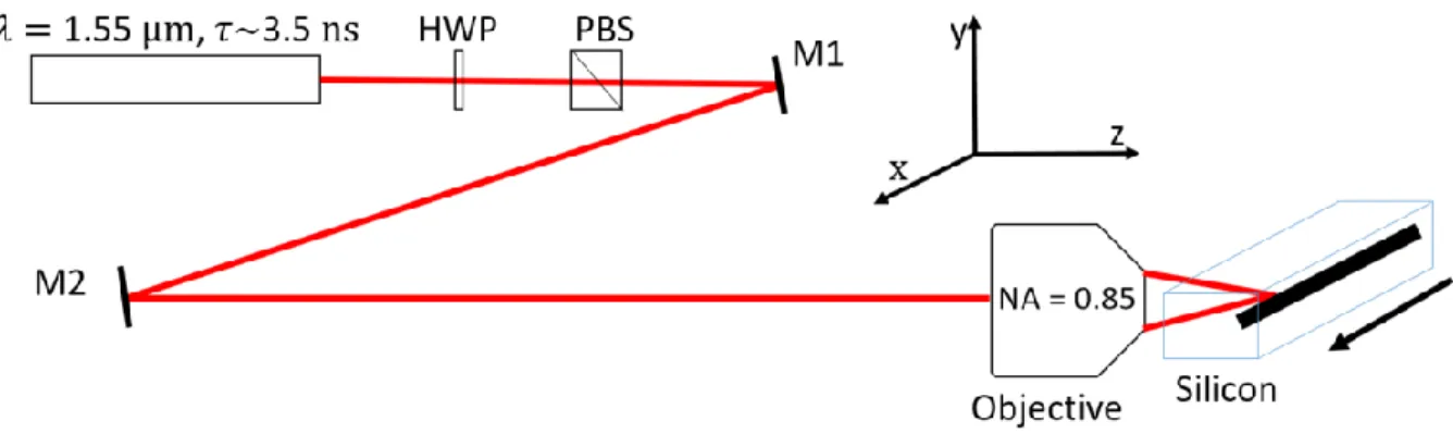
Fig. 1. Experimental setup. M1 and M2 are gold mirrors. HWP and BS are half-wave plate and polarizing beam splitter, respectively.
The experimental arrangement is depicted in Fig. 1. The samples used in this study are (100)-oriented, 1-mm thick intrinsic silicon wafers. The intrinsic samples have a resistivity of >200 Ω∙cm. The laser source (MWTech, PFL-1550) generates pulses at 1550 nm wavelength, and is operated at various repetition rates ranging from 20 to 150 kHz. The pulse duration is τ=3.5 ns (full width at half-maximum). The maximum pulse energy is 20 µJ. The output beam is collimated and has a 1/e2 diameter of 6 mm. The beam is focused
with an infrared objective lens (NA = 0.85, Olympus, Model LCPLN100XIR), which has SA correction for silicon thickness between 0 and 1 mm (adjustable). At the focus, the beam is spatially Gaussian-shaped with a theoretical diameter at 1 𝑒⁄ of 2𝑤2 0 = 1.22 𝜆 NA = 2.2 μm⁄ , with Rayleigh lengths zR(air) = 2.6 μm and 𝑧𝑅 (Si )≈ 9.2 μm in air and silicon, respectively. The wafers are cleaved into small pieces of about
20×20 mm2, which are mounted on a motorized XYZ stage (Newport, Model ILS100PP). The focal depth
is controlled by moving the sample along the laser beam’s axial direction, and modification is induced by scanning the sample transversely at a constant speed. The focus on the front surface is determined when white-light plasma radiation from surface damage is observed, and the desired depth (d) is reached by moving the sample towards the objective by d/n, where n=3.5 is the refractive index of silicon at 1.55 µm. The sample after laser writing is cleaved perpendicularly to the scanning direction and the cross sections (in the (110)-plane) are observed with a visible-light optical microscope. The cleaved surface is then polished and examined with the microscope again. The polished surface is put in a 50 wt. % KOH solution and etched for 5 minutes in an ultrasonic bath. Then the sample is observed with the microscope. In this study, damage is not observed on either front or back surface of the silicon samples. Here, the term “modification” refers to any permanent change in the sample after laser treatment, and “damage” refers to significant modification, such as cracks and voids.
3. Results and discussion
3.1. Optimal focal depth with spherical aberration (SA) correction
Fig. 2. Cross sections of modification lines in silicon at various depths with pulse energy of (a) 2.5 µJ, (b) 2 µJ, and (c) 1.5 µJ. The focusing lens is corrected for spherical aberrations at a depth of 0.5 mm inside silicon (correction collar). Regions in black color and aligned vertically are laser-induced modification. Narrow vertical lines in red color are depth measurements.
Since the difference in refractive index between air and silicon is large, and the beam is focused deep inside the material which extremely increases the spherical aberration, it is necessary to correct spherical aberration. The objective lens used in this study has a correction collar and can compensate aberration in silicon with thickness up to 1 mm. To facilitate later characterization of induced modification, modification is generated in the middle of the samples, and therefore the correction collar is set at 0.5 mm throughout the experiments. However, setting the correction at 0.5 mm does not guarantee optimal focusing at this depth (shown below), since the lens might be designed for a wavelength different from our laser wavelength. To get this optimal focusing depth, continuous lines are made at various depths with 50 µm increments, at a constant speed of 1 mm/s. The samples are then cleaved perpendicularly to the writing direction, and the cross sections are examined with a visible-light microscope. Fig. 2 shows the results for three pulse energies. Regions in black color and aligned vertically are laser-induced modification, and the structures seen outside these regions are caused by the cleaving procedure. Modification is observed within a wider depth range, from 350 to 550 µm, when the pulse energy is 1 µJ. When the energy is reduced to 0.6 µJ, only two
modifications at 400 and 460 µm can be observed. No modification is seen when the pulse energy is reduced to 0.4 µJ, in very good agreement with similar experiments performed with analogous laser facilities [13, 14].
Fig. 3. Calculated focal intensities at various depths inside silicon with the consideration of refractive index mismatch. Z = 0 corresponds to a depth of 430 µm. The intended focal depths are Z = -100, -50, 0,
50 and 100 µm for (a)-(e), respectively. Intensities in all the images are normalized to the peak intensity in (c).
To understand the results in Fig. 2, we calculate the focal shape at various depths, with the consideration of refractive index mismatch. We use the PSF Lab software [18] to obtain focal intensity profiles. The objective lens is assumed to be perfectly corrected for 430 µm thick silicon, and intensities at various depths are calculated, as shown in Fig. 3. We can see that at the depth corresponding to the correction depth (430 µm), the focus is a diffraction-limited spot size consistent with estimation (Fig. 3(c)). When the foci are shifted by about 50 µm ((b) and (d)), the foci are elongated and the peak intensities drop to about 70% of the peak intensity in (c). Further shifting the depth causes even longer foci and lower (35%) peak intensities. This shows that a shift in depth as small as 50 µm can cause reduction of peak intensities and as a consequence disappearance of laser-induced modification, in consistence with the experimental results shown in Fig. 2. We put the laser focus in the optimal depth range of 400 to 460 µm in the following experiments.
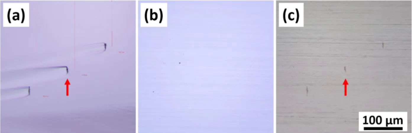
3.2. Observation of modification after polishing and KOH etching
Fig. 4. Cross sections of laser-modified regions after (a) cleaving, (b) polishing, and (c) chemical etching. The laser light is from top to bottom. Two cross sections pointed by arrows are magnified in Fig. 5. Some groups[14-16] directly observe modifications in the bulk. Here, we choose to observe the modification by cleaving the sample, without the limitation in terms of resolution of infrared microscopy. A drawback of this method is that it induces undesired alteration to the samples (Fig. 2). This might be indistinguishable from the modification caused solely by the laser. To avoid confusion, we apply the polishing-and-etching method that is commonly used in the study for dielectrics [21] and has also been used for silicon recently [18]. The sample from the previous experiment (Fig. 2(b), also shown in Fig. 4(a)) is mechanically polished. Interestingly, the modified regions completely disappear after polishing, as shown in Fig. 4(b). A similar behavior is also reported for femtosecond laser writing [15]. For the samples machined by the highest pulse energy (3.75 µJ) and a much slower scanning speed (0.01 mm/s), modification also disappears after polishing (results not shown here). These findings suggest that the laser-induced modification in this study might merely be local change of density [15], not significant damage such as cracks and voids, because otherwise one would expect to see some type of irregularities on the polished surface. The change of density manifests itself after the disturbance during the sample cleaving procedure, and therefore modified regions can be observed in Fig. 4(a). After polishing, we etch the sample by 50 wt.% KOH solution for 5 minutes in an ultrasonic bath. The laser-modified regions reappear as shown in Fig. 4. Meanwhile, the alteration caused by cleaving is absent. Similar etching selectivity is reported in dielectrics [22].
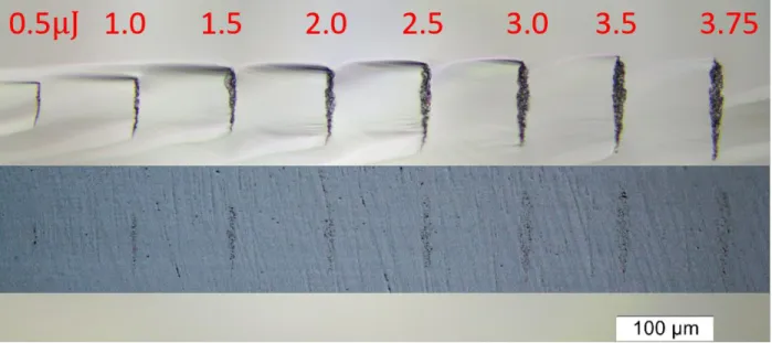
3.3. Morphology of resultant modification
Fig. 5. Laser-induced modification at the same depth (430 µm) and with increasing pulse energy (upper row is after cleaving, and lower row is after polishing and etching). Numbers above the modified regions
represent pulse energy in µJ. The scanning speed is 1mm/s. The laser light is from top to bottom. Laser scanning speed affects the modification morphologies at the same energy density since the speed is related to the number of pulses absorbed by the material based on the equation N=RS/V, where N is the pulse number, R the pulse repetition rate, S the beam focal spot size and V the laser
The absorption of 1.55 µm wavelength light in silicon is a two-photon absorption process. The nature of absorption is complicated since the difference between the photon energy (0.8 eV) and the bandgap (1.1 eV) is small. Previous work shows that the heating of silicon by the laser may cause the bandgap to shrink, leading to linear absorption [16]. Therefore, it is necessary to quantify the size and volume of the absorption regions.
For this purpose, we focus the beam at a fixed depth of 430 µm and write lines with increasing pulse energy. The cross sections treated after the polishing-etching procedure are shown in Fig. 5. As expected, the modifications become larger with increasing pulse energy. The shape of modification is an inverse triangle when the pulse energy is high. We make a simple estimate and find that the energy density in the modified volume is between 0.5 to 4.6 kJ/cm3, orders-of-magnitude below the damage threshold (MJ/cm3
achieve tighter focusing, other mechanisms, such as plasma defocusing [20], might impair the
effectiveness in realizing high energy density. It is critical to understand the fundamental mechanisms in the laser energy deposition process in order to further improve the stealth dicing technique.
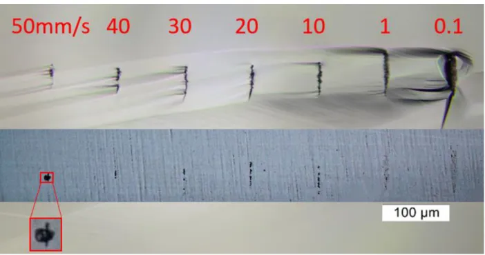
3.4.2 The influence of laser scanning speed on modification morphologies
Fig. 6. Modifications at various scanning speed (upper row is after cleaving, and lower row is after polishing and etching). Pulse energy is 1.5 μJ and repetition rate is 20 kHz. The laser light is from top to
bottom.
Laser scanning speed affects the modification morphologies at the same energy density since the speed is related to the number of pulses absorbed by the material based on the equation N=RS/V, where N is the pulse number, R the pulse repetition rate, S the beam focal spot size and V the laser scanning speed [23]. With fixed pulse energy, repetition rate and focal spot size, the scanning speed is the only parameter that can be varied in order to control the modification shape. Modification length and width at various scanning speeds are shown in Fig. 6. At a low speed (0.1 mm/s), we can observe the modification with the width of 12.5 µm and 68.9 µm, respectively. In particular, at the speed of 10-30 mm/s, the modifications break to several parts. Furthermore, with the speed increasing to 50 mm/s, the modification is almost circular (the length and width are 8.9 µm and 11.3 µm, respectively), which has potential application for waveguide writing inside silicon. Therefore, we can tune the scanning speed to control the modification length and width.
3.4.3 The influence of repetition rate on modification
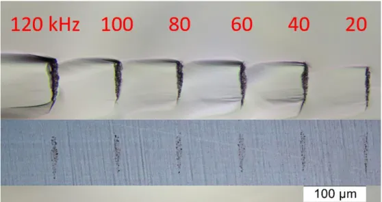
Fig. 7. Modifications at various repetition rate (Up row is after cleaving, and lower row is after polishing and etching). The pulse energy is 1.5 μJ and the scanning speed is 1 mm/s. The laser light is from top to
bottom.
With fixed scanning speed, pulse energy and focal spot size, the repetition rate affects the modification shape. Fig. 7 shows modification length and width at various repetition rates. At a low repetition rate (20 kHz), we can observe the modification with the width of 10 µm and the length of 100 µm. At a higher repetition rate (120 kHz), the length and width increases to 110 µm and 30 µm, respectively.
In Fig. 7, scanning speed is set to 1mm/s, pulse energy is kept at 1.5 μJ , and the focal spot diameter is 2.2 µm. Pulse energy affects morphology of modifications more than repetition rate. For 120 kHz, the length and width of modification are 62.9 µm and 11.9 µm, respectively. For 20 kHz, the length and width of modification are 54.2 µm and 8.7 µm, respectively. Comparing results at 20 kHz and 120 kHz, the repetition rate has a 6-fold difference, while the difference in modification size is significantly less pronounced than varying the pulse energy (Fig. 5).
Fig.8. a, Schematic diagram of the experimental setup with a slit. b, Modifications with and without slit. Up row is without slit, and lower row is with slit. From left to right, the pulse energy is 0.75, 1.0, and 1.25
μJ, respectively. The repetition rate is 20 kHz, and the scanning speed is 10 mm/s. The laser light is from top to bottom.
The dependence of modification morphology on input beam shape is also investigated. Since the sample is translated transverse to the writing beam to form the modification, the cross section is related to the shape of the focal volume. Typically, the focal intensity distribution of a beam focused into a silicon wafer is several times larger in the axial direction than the transverse directions, potentially resulting in highly asymmetric waveguides. To obtain a circular cross sectional profile, one can employ multiple scans of the writing beam across the sample, shifting the beam transversely between each pass [23]. Several methods have been used in the past to shape the writing beam’s focal volume [24]. The simplest of these is to use a physical slit before the objective, effectively reducing the NA in one dimension [25]. In our experiment, we create a slit by two paralleled razor blades. In Fig. 8a, the slit width is set at 1000 µm. We compare the morphology of modification with and without slit under three different pulse energies (0.75, 1.0 and 1.25 μJ ), as shown in Fig. 8b. We can see that the morphology of modification without a slit is much more elongated than with a slit. An aspect ratio close to 1 is expected to be reached if we change the slit width and pulse energy. However, it might be not easy because the refractive index of 3.5 of silicon is so high that the slit width has to be very small, provoking too much energy losses.
4. Conclusion
In conclusion, we use a fiber laser with 1.55 µm wavelength and 3.5 ns pulse duration to generate permanent modification inside intrinsic silicon wafers. Spherical aberration is found to be important and needs to be corrected for tight focusing at desired depth. While laser-induced modification can be clearly observed after cleaving the samples and exposing the cross sections, this modification disappears after mechanical polishing, suggesting the absence of severe damage such as cracks and voids. The morphology of subsurface modification is found to depend on the laser pulse energy, scanning speed, repetition rate and input beam shape. More specifically, the length and width of the modification increase with the increasing pulse energy and repetition rate, but decrease with the increasing scanning speed. The aspect ratio of the modification is affected by the shape of input beam.
References
[1] J. Ikeno, Y. Tani and A. Fukutani: Development of Chipping-Free Dicing Technology Applying Electrophoretic Deposition of Ultrafine Abrasives, Annals of CIRP 41/1 (1992) 351-354.
[2] I.-H. Cho, S.-C. Jeong, J.-M Park and H.-D. Jeong: The Application of Micro-Groove Machining for the Model of PDP Barrier Ribs, Journal of Materials Processing Technology 113 (2001) 355-359
[3] S.B. Lee, Y. Tani, H. Ssato and T. Enomoto: Development of a Dicing Blade with Photopolymeriza Resins for ImprovingMachinability, Annals of CIRP 54/1 (2005) 293-296.
[4] G.C. Lim, A.T. Mai, D. Low and Q. Chen: High Quality Laser Microcutting of Difficult-to-Cut Materials - Copper and Si Wafer, Proceedings of 21st International Congress on Applications of
laser and Electro-Optics, (2002).
[5] F. Fukuyo, K. Fukumitsu and N. Uchiyama: The Stealth Dicing Technologies and Their Application, Proceedings of 6th Laser Precision Microfabrication, (2005).
[6] W. Peng, X.F. Xu and L.F. Zhang: Improvement of a Dicing Blade Using a Whisker Direction-Controlled by an Electric field, Journal of Materials Processing Technology 129 (2002) 377-379. [7] R. Ebutt, S. Danyluk and I. Weisshaus: Method to Evaluate Damage Induced by Dicing and Laser
Cutting of Si Wafers, Microstructural Science 23 (1996) 89-94.
[8] K. Watanabe, Y. Ishizaka, E. Ohmura and I. Miyamoto: Analysis of Laser Ablation Process in Semiconductor Due to Ultrashort Pulsed Laser with Molecular Dynamics Simulation, Proceedings
of SPIE 3933 (2000) 46-55.
[9] P. Chall: ALSI’s Low Power Multiple Beam Technology for High Throughput and Low Damage Wafer Dicing, Proceedings of 65th Laser Materials Processing Conference, (2005), 211-215.
[10] D. Perrottet, A. Spiegel, F. Wagner, R. Housh, B. Richerzhagen and J. Manley: Particle-free Semiconductor Dicing Using the Water Jet Guided Laser Technology, Proceedings of 21st
International Congress on Applications of Lasers and Electro-Optics (2004).
[11] E. G. Gam [10] T. Corboline, C.E. Rea and C. Dunsky: High Power UV Laser Machining of Si Wafers, Proceedings of SPIE 5063, Fourth International Symposium on Laser Precision
Microfabrication, (2003), 495-500.
[12] Chambonneau, M., et al. "Writing waveguides inside monolithic crystalline silicon with nanosecond laser pulses." Optics letters 41.21 (2016): 4875-4878.
[13] Yu, X., Wang, X., Chanal, M., Trallero-Herrero, C. A., Grojo, D., & Lei, S. (2016). Internal modification of intrinsic and doped silicon using infrared nanosecond laser. Applied Physics
A, 122(12), 1001.
[14] P. C. Verburg, G. R. B. E. Römer, and A. J. Huis in ’t Veld, “Two-photon–induced internal modification of silicon by erbium-doped fiber laser,” Opt. Express, vol. 22, no. 18, pp. 21958– 21971, 2014.
[15] M. Mori, Y. Shimotsuma, T. Sei, M. Sakakura, K. Miura, and H. Udono, “Tailoring thermoelectric properties of nanostructured crystal silicon fabricated by infrared femtosecond laser direct
writing,” Phys. Status Solidi, vol. 7, pp. 1–7, Jan. 2015.
[16] Y. Ito, H. Sakashita, R. Suzuki, M. Uewada, K. P. Luong, and R. Tanabe, “Modification and machining on back surface of a silicon substrate by femtosecond laser pulses at 1552 nm,” J.
Laser Micro Nanoeng., vol. 9, no. 2, pp. 98–102, 2014.
[17] D. Grojo, A. Mouskeftaras, P. Delaporte, and S. Lei, “Limitations to laser machining of silicon using femtosecond micro-Bessel beams in the infrared,” J. Appl. Phys., vol. 117, p. 153105, 2015. [18] M. J. Nasse and J. C. Woehl, “Realistic modeling of the illumination point spread function in
confocal scanning optical microscopy,” J. Opt. Soc. Am. A, vol. 27, no. 2, pp. 295–302, Jan. 2010. [19] X. Yu, Y. Liao, F. He, B. Zeng, Y. Cheng, Z. Xu, K. Sugioka, and K. Midorikawa, “Tuning etch
selectivity of fused silica irradiated by femtosecond laser pulses by controlling polarization of the writing pulses,” J. Appl. Phys., vol. 109, no. 5, p. 053114, Mar. 2011.
[20] E. V Zavedeev, V. V Kononenko, and V. I. Konov, “Delocalization of femtosecond laser radiation in crystalline Si in the mid-IR range,” Laser Phys., vol. 26, no. 1, p. 016101, 2016.
[21] S. Leyder, D. Grojo, P. Delaporte, W. Marine, M. Sentis, and O. Utéza, “Non-linear absorption of focused femtosecond laser pulses at 1.3μm inside silicon: Independence on doping concentration,”
Appl. Surf. Sci., vol. 278, pp. 13–18, 2013.
[22] R. Osellame, H.J.W.M. Hoekstra, G. Cerullo, M. Pollnau, Femtosecond laser microstructuring: an enabling tool for optofluidic lab-on-chips. Laser Photonics Rev. 5, 442–463 (2011)
[23] R. Le Harzic, D. Breitling, M. Weikert, S. Sommer, C. Fohl, S. Valette, C. Donnet, E. Audouard, F. Dausinger, Pulse width and energy influence on laser micromachining of metals in a range of 100 fs to 5 ps. Appl. Surf. Sci. 249 (2005) 322-331.
[24] Nasu, Y., Kohtoku, M. and Hibino, Y., 2005. Low-loss waveguides written with a femtosecond laser for flexible interconnection in a planar light-wave circuit. Optics letters, 30(7), pp.723-725. [25] M. Ams, G. D. Mars hall, D. J. Spence, and M. J. Withford, Slit beam shaping method for
femtosecond laser direct-write fabrication of symmetric waveguides in bulk glasses. Opt. Express 13, 5676 (2005).