An ARM-Based Sequential Sampling Oscilloscope
ByQiaodan (Jordan) Jin Stone
S.B., E.E. Massachusetts Institute of Technology, 2013
Submitted to the Department of Electrical Engineering and Computer Science in Partial Fulfillment of the Requirements for the Degree of
Master of Engineering in Electrical Engineering and Computer Science at the Massachusetts Institute of Technology
September 2014
©Massachusetts Institute of Technology, 2014. All rights reserved. The author hereby grants to M.I.T. permission to reproduce and to distribute publicly paper and electronic copies of this thesis document in whole and in part
in any medium now known or hereafter created.
Author: ________________________________________________________ Department of Electrical Engineering and Computer Science Aug 22, 2014
Certified by: ____________________________________________________
Gerald Jay Sussman
Panasonic Professor of Electrical Engineering
Thesis Supervisor
Accepted by: ___________________________________________________ Prof. Albert R. Meyer Chairman, Masters of Engineering Thesis Committee
An ARM-Based Sequential Sampling Oscilloscope
ByQiaodan (Jordan) Jin Stone
Submitted to the Department of Electrical Engineering and Computer Science August 22, 2014
In Partial Fulfillment of the Requirements for the Degree of Master of Engineering in Electrical Engineering and Computer Science
Abstract
Sequential equivalent-time sampling allows a system to acquire repetitious waveforms with frequencies beyond the Nyquist rate. This thesis
documents the prototype of a digital ARM-based sequential sampling oscilloscope with peripheral hardware and software. Discussed are the designs and obstacles of various analog circuits and signal processing methods. By means of sequential sampling, alongside analog and digital signal processing techniques, we are able to utilize a 3MSPS ADC for a capture rate of 24MSPS. For sinusoids between 6-12MHz, waveforms acquired display at least 10dB of SNR improvement for unfiltered signals and at least 60dB of SNR improvement for aggressively filtered signals. Thesis Supervisor: Gerald Jay Sussman
Acknowledgements
My experience here would not have been possible without the generous donations of various organizations internal and external to MIT. Thank you all so much for this opportunity.
I’d like to thank the MIT Electronics Research Society (MITERS) for giving me the confidence to learn (and hack) … well anything. I’ll never forget my first blinky LED, first time I turned on (and fell off) Segboard, the F21 “shopping” trip, mountains of etched PCBs, the time Babycopter bit my finger, and all the other absurd, happy memories. Thank you all for taking me in sophomore year. I hope MITERS exists for decades to come and continues to foster the spirit of engineering in each new generation. Speaking of MITERS, I’d like to particularly thank Charles Guan and Shane Colton for their friendship, guidance, and nearly infinite
patience. I wouldn’t have been half the engineer (or human being) without you two. Thank you for helping me gain the courage to go build.
My gratitude to Taylor Barton and Zhen Li for my excellent circuits education. Just so you know, me being analog is your fault.
A big thanks to Joseph Colosimo whose unwavering support,
encouragement, and cheer has kept me sane the last three years. You’re the best Joe.
I’d like to thank Prof. Sussman for taking the role of advisor quite literally and offering me guidance not only in debugging circuits, but also in debugging life.
Lastly, thank you Dad for all the sacrifices you’ve made. I wouldn’t have gotten this far without you. I know I don’t tell you this enough, but you really are my role model. Thanks for always accepting the unfiltered, unaltered me. Shin-Kay-Low.
Table of Contents
1 Introduction ... 9
1.1 Educational Lab Equipment ... 9
1.2 Previous Personal Computer Oscilloscopes ... 10
2 Oscilloscope Sampling ... 11
2.1 Real-Time Oscilloscopes ... 11
2.2 Sequential Equivalent-Time Sampling Oscilloscopes ... 13
3 Input Attenuator and Gain Circuit ... 17
3.1 Input Stage ... 17
3.1.1 Input Signal Attenuator ... 17
3.2 Input Gain Pre-Amp ... 20
3.2.1 Bandwidth ... 22 3.2.2 Slew Rate ... 26 4 Trigger Circuit ... 28 4.1 Overview ... 28 4.1.1 Comparator ... 28 4.1.2 Pre-Amplifier ... 29 4.1.3 Hysteresis ... 31 5 Firmware Architecture ... 33 5.1 libopencm3 ... 33
5.2 Signal Chain (Real-Time Sampling) ... 33
5.3 Signal Chain (Sequential Sampling) ... 35
5.4 Trigger-Timer Subsystem ... 37 5.4.1 Timer Setup ... 37 5.4.2 Phase Subsystem ... 40 5.5 ADC-DMA Subsystem ... 43 5.5.1 ADC ... 43 5.5.1.1 ADC Off ... 43 5.5.1.2 ADC On/Unpaused ... 45 5.5.1.3 ADC Paused ... 47
5.5.1.4 ADC Register Settings ... 49
5.6 DMA Register Settings ... 51
5.6.1 DMA – ADC Module ... 53
5.6.2 USB ... 55
5.6.3 Summary ... 55
6 Signal Processing ... 56
6.1 Signal Chain ... 56
6.2 MATLAB Reconstruction ... 60
6.2.1 MATLAB Code Overview ... 60
6.2.1.1 Data Packet ... 60
6.2.1.1.1 Fast Fourier Transform ... 62
6.2.1.2 Signal Reconstruction Overview ... 66
6.2.1.3 Signal Reconstruction Issues ... 68
6.2.1.3.1 Moiré Patterns ... 68
6.2.1.4 Signal Reconstruction Later Improvements ... 69
7 Data and Specs ... 70
7.1 Overall Performance (Input Stage + ARM) ... 70
7.1.1 Normal \ Real-Time Mode ... 70
7.1.1.1 Signal Path Description ... 70
7.1.1.2 Issues ... 80
7.1.2 Sequential Mode ... 80
7.1.2.1 Signal Path Description ... 80
7.2 Data Without Gain Circuit (ARM only) ... 94
7.2.1 Normal Mode ... 94 7.2.2 Sequential Mode ... 98 7.3 Issues ... 102 8 Future Considerations ... 103 8.1 Analog Improvements ... 103 8.2 Digital Improvements ... 103
8.3 Signal Processing Improvements ... 104
8.4 Signal Generator ... 104
8.5 Over-Voltage ... 106
8.6 GUI/Automated Software ... 107
9 Conclusion ... 108
10 Firmware Appendix ... 109
10.1 Firmware for STM32F3 Discovery Development Board ... 109
11 Software Appendix ... 125
11.1 Python USB interface ... 125
11.2 MATLAB Signal Reconstruction ... 127
11.2.1 Sinc Filter Program ... 127
11.2.1.1 Conv_fft.m ... 127
11.2.1.2 Sinc_filter.m ... 130
11.2.2 Sinc Interpolation Program ... 133
11.2.3 Real-Time (Normal) Mode ... 134
Table of Figures and Tables
Figure 2-1. Output signal displays aliasing if input frequency higher than Nyquist cutoff
[3]. ... 12
Figure 2-2. Sampling clock must be fast enough to capture edge transitions [3]. ... 12
Figure 2-3 Buffer Memory Depth vs. Sampling Clock Diagram ... 13
Figure 2-4 ... 14
Figure 2-5 ... 14
Figure 2-6 ... 15
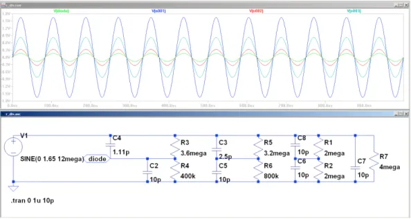
Figure 2-7. Overall System Block Diagram and schematic. ... 16
Figure 3-1. Input attenuator (probe). ... 17
Figure 3-2. Uncompensated probe simulation. Input signal is a 50kHz sine wave with 3.3Vpp. Displayed waveforms are for the four attenuator outputs. As noted, 1/2, 1/5, and 1/10 create a low-pass effect (middle graphs). ... 19
Figure 3-3. Compensated probe simulation. Input signal is 12MHz sine wave with 3.3Vpp. Displayed waveforms are for the four attenuator outputs. With proper tuning 1/2, 1/5, and 1/10 (middle graphs) display no filtering. ... 19
Figure 3-4. Gain system. ... 20
Figure 3-5, AD8032 [5] ... 21
Figure 3-6, AD823 Datasheet [6] ... 22
Figure 3-7 ... 23
Figure 3-8 [7]. From Kent Lundberg, "Internal and External Op-Amp Compensation: A Control-Centric Tutorial ," in American Control Conference, vol. 6, Boston, 2004 , pp. 5197 - 5211. ... 24
Figure 3-9 AD8032 [5] ... 25
Figure 3-10, AD823 Datasheet [6] ... 25
Figure 3-11. Input Signal =1Vpp x 2 Gain at 8MHz. Notice DC shifts for each trace. Green (top) is TP2. Pink (middle) is TP2 with an additional 1.5V offset. Yellow (bottom) is TP1. All test point locations are documented in Fig 2-7. ... 26
Figure 3-12. 1Vpp x 2 Gain, 4MHz ... 27
Figure 4-1. 5MHz sine at 500mVpp. Green is the trigger voltage selected by the user. ... 29
Figure 4-2. Instrumentation Amplifier ... 30
Figure 4-3. Instrumentation amp with windowing diodes. ... 31
Figure 4-4. Trigger with hysteresis. ... 32
Figure 5-1. Flow chart for real-time sampling. ... 34
Figure 5-2. Flow chart for sequential sampling. ... 36
Figure 5-3, from the STM32F3 Reference Manual [9] ... 38
Figure 5-4. Timer Connection Diagram. ... 40
Figure 5-5. Firmware timing diagram. ... 42
Figure 5-6. Flow chart for ADC Off. ... 44
Figure 5-7. Flow chart for turning ADC On/Unpaused. ... 46
Figure 5-8. Flow chart for pausing ADC. ... 48
Figure 5-10. ADC EXTi List. ... 50
Figure 5-11. DMA Block Diagram. ... 52
Figure 5-12. Flow chart for ADC-DMA subsystem. ... 54
Figure 6-1. Frequency domain description of process. ... 57
Figure 6-2 ... 58
Figure 6-3. 2Vpp sine input at 4MHz. ... 58
Figure 6-4. Data Packet Structure. ... 61
Figure 6-5, William Siebert, Circuits, Signals, and Systems. Cambridge, MA, USA: The MIT Press, 1986. [10] ... 63
Figure 6-6. MATLAB code outline. ... 67
Figure 6-7. Moiré Patterning. ... 68
Figure 7-1. 100kHz sine wave. 500mVpp. SNR raw = 33.90dB. SNR interpolated = 37.3dB. ... 71
Figure 7-2. 600kHz sine wave 500mVpp. SNR raw = 23.18dB. SNR interpolated = 29.82dB. ... 72
Figure 7-3. 1.2MHz sine wave 500mVpp. SNR raw = 16.44dB. SNR interpolated = 24.36dB ... 73
Figure 7-4. 1.4MHz sine wave 500mVpp. SNR raw = 15.15dB. SNR interpolated = 22.63dB. ... 74
Figure 7-5. 100kHz triangle. 500mVpp. ... 76
Figure 7-6. 400kHz triangle. 500mVpp. ... 77
Figure 7-7. 100kHz square. 500mVpp. ... 78
Figure 7-8. 400kHz square. 500mVpp. ... 79
Figure 7-9. Eight gels of 1.5MHz unfiltered sine wave with 800mVpp. ... 81
Figure 7-10. Brick wall filter moves depending on center frequency. ... 82
Figure 7-11. 1.5MHz-unfiltered sine wave with 800mVpp. FFT after 2 times interpolation. ... 82
Figure 7-12. 1.55MHz-unfiltered sine 800mVpp reconstructed and FFT. Pre-Interpolated Data SNR = 9.05dB. Sinc-Pre-Interpolated SNR = 26.6dB. ... 82
Figure 7-13. 1.5MHz Filtered sine wave with 800mVpp. FFT after 2 times interpolation. Bottom FFT is after sinc-filtering with brick wall at center frequency (frequency of largest coefficient). ... 83
Figure 7-14. 1.5MHz Filtered sine wave 800mVpp reconstructed and FFT. Pre-Interpolated Data SNR = 9.05dB. Sinc-Pre-Interpolated SNR = 69dB. ... 83
Figure 7-15. 1MHz Unfiltered sine 500mVpp reconstructed and FFT. Pre-Interpolated Data SNR = 12.7dB. Sinc-Interpolated SNR = 21.35dB. Blips are from trigger noise. ... 85
Figure 7-16. 3MHz Unfiltered sine 400mVpp reconstructed and FFT. Pre-Interpolated Data SNR = 2.02dB. Sinc-Interpolated SNR = 43.87dB. Blips are from trigger noise. ... 86
Figure 7-17. 6MHz Unfiltered sine 400mVpp reconstructed and FFT. Pre-Interpolated Data SNR = -3.56dB. Sinc-Interpolated SNR = 13.66dB. ... 87
Figure 7-18. 9MHz unfiltered sine 200mVpp reconstructed and FFT. Pre-Interpolated Data SNR = -7.33dB. Sinc-Interpolated SNR = 7.12dB. ... 88
Figure 7-19. 11MHz Unfiltered sine 200mVpp reconstructed and FFT. Pre-Interpolated Data SNR = -4.82dB. Sinc-Interpolated SNR = 5.57dB. ... 89
Figure 7-20. 400kHz Square. 500mVpp. ... 90
Figure 7-22. 3MHz Square. 500mVpp. ... 92
Figure 7-23. 3MHz Triangle. 500mVpp. ... 93
Figure 7-24. 100kHz sine wave 500mVpp. SNR raw = 31.76dB. SNR Interpolated = 34.08dB. ... 95
Figure 7-25. 600kHz sine wave 500mVpp. SNR raw = 26.06dB. SNR Interpolated = 36.04dB. ... 96
Figure 7-26. 1.2MHz sine wave 500mVpp. SNR raw = 20.6dB. SNR Interpolated = 28.96dB. ... 97
Figure 7-27. 3MHz sine wave 400mVpp. SNR raw = 4.39dB. SNR interpolated = 26.22dB. ... 99
Figure 7-28. 6MHz sine wave 400MVpp. SNR raw = -0.99dB. SNR interpolated = 10.09dB ... 100
Figure 7-29. 9MHz sine wave 200mVpp. SNR raw = -3.54dB. SNR interpolated = 6.09dB. ... 101
Figure 8-1. Output waveform selected by three buttons. The pull-up resistors for each GPIO sets the default “off” state as high. ... 105
Figure 8-2. ADC voltage controls time step value. ... 105
1 Introduction
1.1 Educational Lab Equipment
A recent trend in education is massive open online courses
(MOOCs). Universities such as MIT, Harvard, UC Berkeley, and Stanford have begun developing large online classes based on a limited selection of their course catalogs. These classes are offered from a variety of technical fields: mechanical engineering, computer science, mathematics, etc. A
challenge for these courses is providing hands-on experience for classes that would traditionally have a lab component.
For electrical engineering classes, basic lab equipment such as oscilloscopes and signal generators often easily cost thousands of dollars. Students enrolled in an online course may not have access to a university or hackerspace that could provide such test equipment. Most students cannot purchase such lab equipment. Furthermore, swapfests and eBay are not viable options for beginners to hunt down niche gear, nor are such vendors guaranteed to be globally available.
I have experimented with the design and implementation of a small, affordable digital oscilloscope based off an ARM architecture
microcontroller. The parts are generic, ensuring students access to electronic component vendors online through which they could purchase microcontrollers and oscilloscope peripherals. Additionally, students are then capable of individually installing oscilloscope firmware in the comfort of their own homes. Thus, an oscilloscope based on a common ARM microcontroller would permit students not only to own lab equipment, but also a platform from which they could learn microcontroller programming and build other personal projects. The overall cost of the oscilloscope and
signal generator system should be relatively affordable ($10-$30) with free and accessible example code for future individuals to update and modify.
1.2 Previous Personal Computer Oscilloscopes
Several other oscilloscope microcontroller projects already exist. The majority are software projects with an oscilloscope GUI and a simple PCB to test basic circuit connections. An ADC directly contacts the point of interest with a microcontroller buffering a set of sampled information to a screen. Very little to no signal processing is applied to the collected signal, and the system is bandwidth limited by the input ADC.
While this simplified digital system is perfect for electronics enthusiasts, I intend to deliver a more sophisticated hardware system complete with protection and trigger circuits and basic signal processing. Most importantly, I intend to implement sequential sampling, allowing an input signal to be faster than our Nyquist cut-off frequency.
Unfortunately, my experiments were not entirely successful. While I did create a system that samples at 24MSPS, 6MHz – 12MHz has far worse SNR than the first 6MHz. In addition, grounding and shielding issues plagued the input analog circuits – the “digital” trigger output coupled into the analog signal input and produced spikes with some
ringing. In this document I explain what I tried, what worked and what did not, and what I learned from the experience.
2 Oscilloscope Sampling
In order to achieve a bandwidth higher than specified by our local ADC, a sequential sampling technique is implemented.
Two popular signal acquisition techniques are real-time and sequential equivalent-time sampling. Each has a specific set of pros and cons.
2.1 Real-Time Oscilloscopes
The concept behind the real-time oscilloscope (RTO) is
straightforward. Signal capture is performed in one contiguous stream. The signal bandwidth must be below the Nyquist sampling frequency of the input signal path (typically an ADC with a sample and hold) as seen in Fig 2-1 and Fig 2-2 [1]. On some systems, the signal is captured and stored continuously, allowing a buffer to contain signal information before and after a trigger event. As such, it is possible for an RTO to operate without a trigger circuit; we are simply loading a FIFO and displaying buffer
information. A trigger level can be set externally through software if desired and needs not exist in hardware.
Another characteristic of RTOs is their “one-shot” nature. Signal information is typically stored in some sort of FIFO. As the signal is collected, the buffer is filled. This acquisition can be done specifically for a transient one-shot or repetitively. The buffer also ensures that all transient signals are preserved without additional signal processing. However, due to this buffer architecture, one problem is memory depth as demonstrated in Fig 2-3. During a single buffer acquisition, one obtains all points for that waveform. Therefore memory depth limits the time resolution of our capture signal [2]. For example, were we to have 1000 points in memory,
we could either store 1µs worth of signal at 1GSPS or 2µs worth of signal at 500MSPS. To store more time, one must either obtain more memory or operate at a slower sampling frequency. Due to these design considerations, RTOs tend to utilize faster, yet lower resolution ADCs [2].
Figure 2-1. Output signal displays aliasing if input frequency higher than Nyquist cutoff [3].
Figure 2-3 Buffer Memory Depth vs. Sampling Clock Diagram
Thus the distinct advantages of RTOs are: trigger circuits are not necessary; one may look ahead and behind a “trigger” event in the stored buffer, and transient events are easily stored and captured. Disadvantages include finite buffer memory depth and constrained sampling rates and bandwidths [1].
2.2 Sequential Equivalent-Time Sampling Oscilloscopes
Unlike real-time sampling, sequential sampling allows an oscilloscope to capture an input signal much greater than Nyquist. Outlines for
techniques similar to sequential sampling exist since the 1960s [4]. By inserting a systematic phase delay in the sampling clock, one can amass a set of sampled data with a higher bandwidth than the original sample rate.
ADC
ADC
2XClock
Fig 2-4 demonstrates the first procedural step of sequential sampling. The input signal is first sampled by the ADC and digitized by a sampling rate clock (that is much slower than Nyquist). As expected, aliasing of the signal occurs. This data stream is then stored in memory and the ADC configures itself to capture another stream of the same input signal but with an added phase offset to the previous sample clock.
Figure 2-4
The clock delay allows us to collect another set of samples (Fig 2-5). This sample set again displays aliasing; we have not changed the clock frequency. However, this aliased data is different from our previous aliased set (Fig 2-6).
Figure 2-5
We then iterate through this process adding a constant phase delay for each trial (until our total phase is 360°). Ultimately, we merge all the individual sets of captured data into one total output signal. This master output signal then contains data with time-steps proportional to the difference of phase delays. As shown in Fig 2-6, the end effect is a sample
ADC
Sampled during rising edge
ADC
rate much higher than our original clock frequency (and permissible ADC bandwidth).
Figure 2-6
While this process significantly improves the sample rate, there are limitations. The input signal must be repetitious; we must sample several phase-delayed copies. In addition, precise timing is critical and a trigger mechanism is required. Lastly, one must have enough memory to store several data sets.
Our oscilloscope allows students to surpass the onboard ADC sampling rate of 3MSPS. The oscilloscope system is composed of four main sections: 1) input attenuator, 2) gain circuit, 3) trigger circuit, 4) firmware for sequential sampling and USB communication. Fig 2-7 is a large block diagram and schematic depicting the connections of the systems.
3 Input Attenuator and Gain Circuit
3.1 Input Stage
High input impedance is necessary to capture signals without excessive loading of the signal source. However, all physical attenuators exhibit some amount of reactive impedance. We should expect the input attenuators to display low-pass filter behavior.
3.1.1 Input Signal Attenuator
Our attenuator approximates a passive scope probe. The circuit maintains total 1MΩ input impedance with four different levels of attenuation: 1/10, 1/5, 1/2, 1.
Fig 3-1 presents our attenuator system. A single-pole four-throw switch selects the attenuation level. This switch is connected to four different resistor dividers similar to traditional analog attenuators. An op-amp generates a virtual ground of half-rail. This virtual ground is connected to the output of the system under test (SUT), giving us an additional half-rail voltage bump – critical for our system as the SUT may center at 0V. Our ADC cannot accept negative values - a virtual ground is essential. Clipping diodes are connected to the pole of the switch to prevent the signal from rising above 0V-3.6V (the ADC maximum input voltage is 4V).
Unfortunately the clipping diodes present capacitance. Each 1N4001 diode has 15pF of junction capacitance, creating a low-pass filter for gains 1/10, 1/5, 1/2 (Fig 3-2). To remove this low-pass filter, a compensation capacitor must be placed between the pole of the switch and the positive line of the SUT (Fig 3-1). This variable trimmer capacitor should only be a few pF and allows the user to tune the top impedance of each resistor divider to match the bottom impedance of each resistor divider – we are compensating the bottom impedance’s pole by placing the top impedance’s zero at the same location. If the capacitor is chosen correctly, the signal should pass through without filtering (Fig 3-3). In a traditional analog scope, we would calibrate our probe with a well-defined square wave. We would then carefully tune the variable cap by observing the step response of the probe. The user could use a low-frequency square wave for such fine-tuned capacitor adjustments, or the user could use a pre-defined and well-characterized sine wave and test for the appropriate level of magnitude attenuation on the scope.
Figure 3-2. Uncompensated probe simulation. Input signal is a 50kHz sine wave with 3.3Vpp. Displayed waveforms are for the four attenuator outputs. As noted, 1/2, 1/5, and 1/10 create a
low-pass effect (middle graphs).
Figure 3-3. Compensated probe simulation. Input signal is 12MHz sine wave with 3.3Vpp. Displayed waveforms are for the four attenuator outputs. With proper tuning 1/2, 1/5, and 1/10
3.2 Input Gain Pre-Amp
The input pre-amplifier for our adjustable gain is a simple non-inverting op-amp gain circuit (Fig 3-4). This is to ensure the amplification of not only small signal AC waveforms, but also DC voltages. The feedback resistor is a single-pole four-throw switch with one percent resistors of 1Ω, 1kΩ, 4kΩ, and 9kΩ (offering gains of 1, 2, 5, 10). Clipping signal diodes are present to prevent the ADC from experiencing overvoltage.
Figure 3-4. Gain system.
AD8032 and AD823 are selected for their unity gain bandwidth and DIP packages. All circuits for this oscilloscope are dead-bugged (due to complex routing for proper high-frequency PCBs, and the technique’s low parasitic capacitance and fast production time). Unfortunately, these op-amps have difficulty with large signals and slewing. However they only require 3V power supplies.
The AD8032 is a BJT op-amp with an 80MHz unity gain bandwidth (Fig 3-5). The AD823 is a JFET input op-amp with 16MHz unity gain bandwidth (Fig 3-6). Due to BJT inputs, the AD8032 has low differential
input impedance – about 280kΩ. The minimal impedance for any of the resistor dividers of the attenuator is 400kΩ, so an AD823 is used as a buffer for the AD8032. An AD823 is also placed after the AD8032 to provide additional low-pass filtering for signals below 16MHz.
A few small gain bumps of ~1dB exist near 9-10MHz for AD823 and 11-12MHz for A8032. They produce a slight amplification towards the upper ends of our frequency range. However, more problematic are the slew rates and bandwidths for gains larger than unity.
Figure 3-6, AD823 Datasheet [6]
3.2.1 Bandwidth
The system bandwidth changes depending on the user selected gain. This is due to the feedback nature of our op-amp circuit.
For our gain circuit, varying the amount of feedback allows us to adjust our overall gain (Fig 3-4). Concurrently, this gain change also alters our feedback dynamics (Fig 3-7).
𝐴 𝑠 is the representation of our op-amp in the frequency domain. Typically 𝐴 𝑠 is represented as a first-degree low-pass filter roughly characterized as !"#$ !""# !"#$
! !!∗ !"#$ !"#$%&$'! !"#$%&' !"#$ !""# !"#$ . Fig 9 and Fig
3-10 depict the 𝐴 𝑠 bode plots for our op-amps. Altering the resistor divider controlling our feedback voltage manipulates our bandwidth (Fig 3-7). The largest bandwidth is at unity gain, for the resistor ratio is !!!!!!!!! ≅ 1. This is evident in the of 𝐿 𝑠 , loop transmission, bandwidth of Fig 3-8. For a gain of 1, F = 1; we have the top graph (blue). However, as we increase the
overall system gain of our op-amp circuit, we reduce the size of our resistor feedback divider. For example, a gain of 10 requires a resistor divider of
!!! !!!!!!! ≅
!
!". This modifies 𝐿 𝑠 to now be !
!"∗ 𝐴 𝑠 . Our new plot is the
second to top graph (green). As we increase the overall gain, our bandwidth decreases (Fig 3-8)
Figure 3-8 [7]. From Kent Lundberg, "Internal and External Op-Amp Compensation: A Control-Centric Tutorial ," in American Control Conference, vol. 6, Boston, 2004 , pp. 5197 - 5211.
This presents an obstacle in terms of bandwidth. While our gain of 1 and 2 are capable of over 12MHz, our gain of 5 barely achieves 12MHz and our gain of 10 is capable only of ~2MHz.
Gain (small signal)
Gain 1 Gain 2 Gain 5 Gain 10
3dB
Frequency
Figure 3-9 AD8032 [5]
3.2.2 Slew Rate
The other main issue for our input amplifier is the slew-rate that produces our maximum slope limitation.
The slew rate for the AD8032 is 30 V/µs and for the AD832 is 20 V/µs [5] [6]. Unfortunately, the slew-rate greatly constricts our signal range. We see signal distortion above these slew specs.
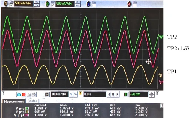
Figure 3-11. Input Signal =1Vpp x 2 Gain at 8MHz. Notice DC shifts for each trace. Green (top) is TP2. Pink (middle) is TP2 with an additional 1.5V offset. Yellow (bottom) is TP1. All test point
locations are documented in Fig 2-7.
TP2 TP2+1.5V
In Fig 3-11, the input signal is originally a 1Vpp sine wave at 8MHz. The bottom signal (yellow) represents the signal after the first unity gain AD832 buffer (Fig 3-4). We can already see some slew distortion. The middle graph (pink) is the signal with a virtual ground of half the rail, and the top graph (green) is the same signal without the virtual ground. The pink and green signals materialize as triangle waves rather than sines.
Figure 3-12. 1Vpp x 2 Gain, 4MHz
Although Fig 3-12 has a slower input signal, we still see slew distortion, in part due to the AD823 only having 16MHz bandwidth for
200mVpp signals. Moreover, we have around a 10pF load from the clipping
diodes for both the attenuator and pre-amplifier. These capacitive loads also decrease our bandwidth for large amplitude signals - we must dump and empty their charge.
TP2 TP2+1.5V
4 Trigger Circuit
4.1 Overview
A trigger circuit is critical for sequential sampling. There are three main sections for the trigger: a comparator, a pre-amplifier, and hysteresis circuit.
4.1.1 Comparator
A comparator is the primary trigger mechanism. The crucial features are propagation and settling time. This is mainly to ensure each trigger occurs quickly and reliably for our sampling frequency of 3MSPS.
Input offset is of some concern as well, however if the input offset is repeatable and well characterized, then triggers will still appear correctly. The main concern for offset is repeatability.
We are using the AD8561 comparator with a 2.3mV input offset with worst-case ~10ns propagation delay at 3V supply with a small hysteresis circuit as shown in Fig 4-4.
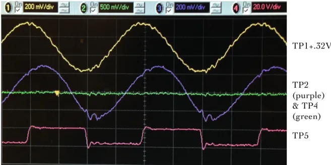
Regrettably, the comparator is a somewhat digital device. Large logic swings produces noise during edge events. This couples into the ADC channel. As seen in Fig 4-1, noise spikes and ringing emerge in the signal path (purple, middle graph) during edges in the trigger signal (pink, bottom graph).
Figure 4-1. 5MHz sine at 500mVpp. Green is the trigger voltage selected by the user.
4.1.2 Pre-Amplifier
The pre-amp is an additional (and optional) add-on for the trigger circuit. As long as the offset for the comparator remains consistent for a fixed input signal, then the overall trigger mechanism will perform
adequately. Should the user wish for a more controlled trigger system, one might implement a pre-amp.
A pre-amp attenuates input referred noise and input referred voltage offset. Often pre-amps are the first input stage of a latched IC comparator as seen in the StrongArm comparator topology [8]. However, we are not interested in IC comparator design. Rather, we wish to improve a pre-existing comparator chip. For a pre-pre-existing discrete comparator, a pre-amp does not have direct access to a latch, and therefore a pre-amp is not
guaranteed to positive feedback. Another challenge is the large common mode range required for use with a discrete comparator. Due to this, a typical differential amplifier is not suggested. However, one could use a windowed instrumentation amplifier (Fig 4-3).
TP1+.32V TP2 (purple) & TP4 (green) TP5
Figure 4-2. Instrumentation Amplifier
The instrumentation amplifier is a suitable proxy pre-amp (Fig 4-2). The amplifier has very low DC input offset, low noise and drift, high input impedance, and high CMRR. The open–loop gain is incredibly large. However, due to its op-amp structure, one must select for speed and
stability. The overall closed-loop gain of the instrumentation amplifier can be fairly small - just enough to boost input signals past the required input offset spec. One should select a conservative closed-loop gain that allows the instrumentation amplifier to remain within the linear regime. This prevents the amplifier from excessive slewing, and thus wasting time.
Figure 4-3. Instrumentation amp with windowing diodes.
4.1.3 Hysteresis
Hysteresis circuits decrease noise near trigger points (Fig 4-4). Two resistors determine the hysteretic loop. The potentiometer (𝑹𝟐) allows the
user to select a trigger voltage. The width of the hysteresis input voltage loop is 𝑹𝑹𝟑
𝟒
𝑽
𝑶𝑯− 𝑽
𝑶𝑳.
For our system 𝑽𝑶𝑯 = 𝟑𝑽 and 𝑽𝑶𝑳 = 𝟎𝑽 and𝑹𝟑 𝑹𝟒
=
!
!"
.
This circuit then generates a rising edge at the user definedtrigger voltage with some added noise immunity due to hysteresis.
A point to note is the trigger voltage exists mainly for signal capture, not as a voltage reference. The trigger voltage must be precise and
repeatable, but not necessarily accurate; we must simply generate an edge for sequential sampling.
5 Firmware Architecture
The firmware consists of four main peripheral systems: ADC, DMA, external trigger/timer, and USB. These four pieces come together to
produce two sampling options: 1) real-time (for signals below the ADC’s inherent Nyquist rate), 2) sequential-sampling (increasing our native 3MSPS to 24MSPS with incremental phase shifts of 42ns). These are then both supplied to the user’s computer whereupon he or she may employ MATLAB or Python to process the raw data signals.
5.1 libopencm3
A peripheral code library created by STMicroelectronics exists for this microcontroller - but in order to use it correctly, a build system such as Keil or Eclipse, is necessary. Libopencm3 is an open source alternative containing peripheral libraries complete with a build system. Firmware can be written in legible C and compiled with GNU Make. Unfortunately, some aspects of libopencm3 are metastable, but the memory mappings are
correct. Register settings are performed through bit assignments mapped to the correct register in the STM32F3’s reference manual.
5.2 Signal Chain (Real-Time Sampling)
For frequencies less than 1.5MHz, real-time sampling is available. In this manner of operation, the ADC is arranged in regular continuous mode, clocking the DMA. This sequence fills a sample buffer that, upon
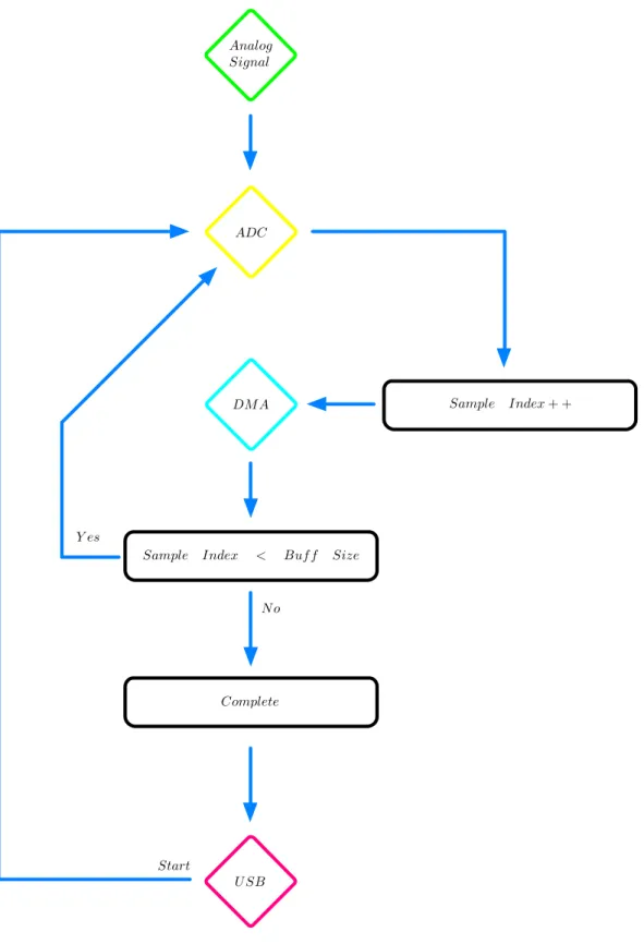
completion, is sent from memory to the USB (Fig 5-1). External triggers during this sequence are ignored. No sequential sampling is used.
Figure 5-1. Flow chart for real-time sampling. Analog Signal U SB ADC DM A Sample Index + +
Sample Index < Buf f Size Y es
N o
Start
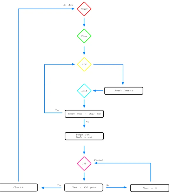
5.3 Signal Chain (Sequential Sampling)
The signal chain for sequential sampling mode is illustrated in Fig 5-2. A user-defined software command arms the trigger for the first sample. An external trigger then initiates the timer that contains the variable for phase. Next, the timer activates the ADC pre-fixed in continuous mode.
Continuous mode allows the ADC to clock the DMA, filling the sample buffer. Once the buffer is full, the data is sent through USB to the user. Afterward, we examine the phase stored in our phase variable. If the phase has not yet reached 360°, we increment the phase by 45° and re-arm the external hardware trigger. After 8 increments of phase, our signal is sequentially sampled at 24MSPS.
The hard-set memory buffer size (due to RAM constraints onboard the microcontroller) can be problematic. One can solve this through further optimization of the USB-laptop communication system. Note: sequential sampling is required only for frequencies above 1.5MHz. The memory buffer should be more than capable of capturing several periods of an >1.5MHz input signal.
Figure 5-2. Flow chart for sequential sampling. T rigger T imer U SB ADC DM A Sample Index + +
Sample Index < Buf f Size Y es
N o
P hase < F ull period
P hase + + Y es N o P hase = 0 Re Arm
F inished Buf f er F ull. Ready to send.
5.4 Trigger-Timer Subsystem
The timer and external trigger systems are interconnected, producing the phase increment mechanism for sequential sampling.
5.4.1 Timer Setup
Our timer (TIM3) must first have the correct settings. From the STM32F3 reference manual [9], we obtain the generalized block diagram of the timer system Fig 5-3. Although the register settings may be somewhat hard to decipher, we utilize only a small section of the overall timer functionality (pink dotted outline).
The main points of interest are: integrating the external trigger (yellow), supplying the counter with the correct phase (green and bottom gold), and connecting the correct interrupt to the ADC (blue).
TIM3_SMCR is the Slave Mode Control Register [9]. To select an external trigger, one must turn on TIM_SMCR_TS_ETRF (External Trigger input (ETRF)) and TIM_SMCR_SMS_TM (Trigger Mode). Note: the trigger event only commands the counter register to begin counting. TIM_SMCR_ETPS_OFF is selected, as we do not need to filter the trigger line. The TIM_SMCR_ETP bit should be zero to ensure that the external trigger polarity is for rising-edge. All other bits in this register can be set to zero as well.
TIM3_CR1 is Control Register 1 [9]. For this register, bits
TIM_CR1_CKD_CK_INT, TIM_CR1_DIR_UP, and TIM_CR1_OPM are set high. TIM_CR1_CKD_CK_INT prevents any clock division. TIM_CR1_DIR_UP directs the counter to count up from 0 to 65535. TIM_CR1_OPM places the timer in pulse/shot mode. The one-shot setting is especially crucial - we must prevent the external trigger from disrupting the ADC-DMA system while collecting a sample buffer.
One-shot is reinitialized upon the completion of each sample buffer, permitting the next phase to be processed.
Figure 5-3, from the STM32F3 Reference Manual [9]
TIM3_CCR1 and TIM3_CNT are Capture/Compare Register 1 and the Counter. TIM3_CCR1 holds the numerical value to which one wishes to count to and TIM3_CNT increments itself until it is the value of
TIM3_CCR1. These two registers hold the phase degree and the counting mechanism to reach the phase.
TIM3_CR2 is control register 2 [9]. In this register we only need TIM_CR2_MMS_COMPARE_OC1REF. This setting brings OC1REF
high when TIM3_CNT equals TIM3_CCR1. Fig 5-4 is part of the “Trigger Controller” block before the TRGO line in Fig 5-3. We see that “the master mode controller” is connected directly to OC1REF. The “master mode controller” is actually a mux controlled by
TIM_CR2_MMS_COMPARE_OC1REF. This mux allows OC1REF to attach directly to TRGO, creating a TRGO event when the OC1REF pin goes high (remember, this occurs when TIM3_CNT equals TIM3_CCR1, indicating we have reached our phase, whether it be 0°, 45°, 90°, 135°, etc.). The only path to the ADC from the timer is through the TRGO line, hence connecting OC1REF to TRGO allows us to control when the ADC conversion sequence begins.
TIM3_CCMR1 is Capture/Compare Mode Register 1. In this register we select TIM_CCMR1_OC1M_PWM2, which specifies that OC1REF is low as long as TIM3_CNT < TIM3_CCR1 and high once TIM3_CNT >= TIM3_CCR1.
TIM3_ARR is the Auto-Reload Register and controls the overall period of the PWM (which we set to the max of 0xFFFF).
TIM3_PSC controls the prescaler for the timer (seen as CK_PSC in Fig 5-3). We have set the prescaler to the default value of one.
TIM3_CCER is the Capture/Compare Enable Register. This can be set to TIM_CCER_CC1E should one wish to see TIM3_TRGO on an external pin for debugging purposes (as seen in Fig 5-4, CC1E sets the subsequent muxes connecting OC1, that can be tied to an external pin, to OC1REF). A pin to use on the STM32F3 Discovery board is PB4 (note: one must then initialize the PB4’s GPIO setting as alternate function two, e.g. GPIO_AF2).
Figure 5-4. Timer Connection Diagram.
5.4.2 Phase Subsystem
The phase increment for sequential sampling is implemented through the timer counter register. The master clock for the STM32F3 is 48MHz. The ADC sample rate is 3MSPS. Given these two conditions, we sample eight phases: 0°, 45°, 90°, 135°, 180°, 225°, 270°, 315°, and 360° - each phase is an additional 42ns. The timing diagram for the phase increments is shown in Fig 5-5 (note not drawn to scale).
Timer 3 (TIM3) is tied to an external trigger circuit that produces falling edges (not shown on diagram) when the input signal reaches the trigger voltage (green dotted line Fig 5-5). This event then activates TIM3’s PWM2 feature (a 16-bit upward counter). Register TIM3_CNT increments until its value matches the number in register TIM3_CCR1. When the two registers are equal, a TIM_TRGO event occurs and a rising edge is
produced on EXT4 (red dashed line Fig 5-5). This then activates the ADC-DMA subsystem that fills a sample buffer (pink dotted box Fig 5-5). Note, should a trigger occur while the ADC-DMA is in the sampling state, it is
ignored. External trigger interrupts are considered invalid until the sample buffer is full.
In the code, each sample buffer is called a “gel” (inspired by the color gels used in theater lighting). Each gel correlates with a phase. When eight gels (and hence eight phases) are collected, we have finished our sequential sampling. To systematically increase the phase, TIM3_CCR1’s value is incremented when the DMA has collected the last sample for a given gel (end of each pink dashed box Fig 5-5). We first begin with TIM3_CCR1 = 0x0h. As 𝟒𝟖𝑴𝑯𝒛
𝟑𝑴𝑯𝒛
=
𝟏𝟔 and we have eight gels, each ofFigure 5-5. Firmware timing diagram. TI M 3 TR G O ev en t on E X T 4 TI M 3 PWM 2 0 1 2 3 4 5 6 7 AD C C a p tu re d W in d ow s In p u t S ig n a l w it h T ri g g er
5.5 ADC-DMA Subsystem
The second large subsystem is our ADC-DMA block. This block captures samples and places them in a buffer, later transmitting them to the user through USB. Sending one ADC sample to the USB at a time is exceedingly slow. Connecting the ADC to the DMA allows us collect a buffer of samples at the maximum ADC sample rate. We then later send them as blocks of data to the USB (which transfers data at a slower rate). We are using ADC1 in regular continuous mode with the DMA in one-shot mode.
5.5.1 ADC
The ADC setup from the reference manual is somewhat difficult to understand and particularly complicated. The ADC is the most complex section of this whole oscilloscope firmware system. Here are some setup elaborations.
5.5.1.1 ADC Off
First, the ADC must be off (not paused) when establishing registers settings. ADC1_CR (control register) controls the bits that activate and disable the ADC. Before attempting any register settings, one must disable ADC_CR_ADEN in ADC1_CR and wait until that bit is cleared by
hardware. Afterwards, set ADC_CR_ADDIS and wait until the bit is cleared. Note: this is the procedure for shutting the ADC off, not pausing the ADC during sampling. The specific procedure is outline in Fig 5-6.
5.5.1.2 ADC On/Unpaused
The ADC on procedure is also very specific (Fig 5-7). The ADC will not activate unless the commands are given in this particular manner.
One must first enable ADC_CR_ADEN then wait until
ADC_ISR_ADRDY is high. After this, the ADC will not capture samples until ADC_CR_ADSTART is set high by the user.
Note: one may pause the ADC during regular continuous mode. In order to un-pause the ADC, this routine must be performed.
Calibration must be completed before the ADC is activated. Simply set ADC_CR_ADCAL in ADC1_CR, and wait until the microcontroller sets the bit in hardware.
5.5.1.3 ADC Paused
Pausing the ADC and disabling the ADC are two different
procedures. One powers off the ADC while the other temporarily suspends ADC capture. Turning the ADC on and off repetitively will erase previous ADC calibrations. Pausing the ADC saves the calibration values from startup.
Pausing is essential for our phase offsets. Each time TIM3_CCR1 is incremented (each time our phase is incremented), we must pause the ADC so as to not collect samples during a phase shift.
First, check that the ADC has already been started (Fig 5-8). Then set the ADC_CR_ADSTP bit and wait until the microcontroller clears it in hardware. Next, ADC_CR_ADDIS must be set, and we must again wait for the ADC_ADEN bit to be cleared by the microcontroller before we can safely assume the ADC is paused.
5.5.1.4 ADC Register Settings
The STM32F3 has four sophisticated ADCs (Fig 5-9). Unfortunately, this causes registers settings to be quite complex.
ADC1_CFGR is the main register for ADC1 settings unrelated to activation/deactivation or interrupts. In this register, we must set
ADC_CFGR_CONT (continuous mode), ADC_CFGR_DMAEN (DMA enabled NOT in circular buffer mode), and ADC_CFGR_RES_8_BIT (8-bit ADC data).
We must also be careful in configuring the ADC trigger. We use TIM3, therefore we must remap TIM3’s TRGO event to the ADC. From Fig 5-9, we see that the ADC can be triggered off of a selection of EXTi (external pin triggers). Listed in the reference manual is a set of external interrupt mappings (Fig 5-10). For this design, we used
ADC_CFGR_EXTSEL_EVENT_4 configured with a rising edge
(ADC_CFGR_EXTEN_RISING_EDGE), as TRGO and OC1REF are connected together and go high when the counter has reached its specific phase.
Figure 5-10. ADC EXTi List.
ADC1_SMPR1 is the Sample Time Register that controls the time between each ADC sample in continuous mode (e.g. sampling rate). Note: there are actually two sample time registers for each of the four ADCs (SMPR1 and SMPR2). This is due to the fact that each ADC has several multiplexed inputs (up to 14 for ADC1 on the STM32F3 Discovery Dev
Board). Other ADCs can have up to 18 multiplexed inputs. One must index into the correct bits for the channel(s) one intends to use. Hence settings for SMPR must be bit-shifted for the correct channel.
The general formula for sample rate is thus:
𝑻𝒄𝒐𝒏𝒗=
(𝑺𝑴𝑷𝑹 + 𝑩𝑰𝑻𝑺 + 𝟎. 𝟓) 𝑹𝑪𝑪 𝑪𝒍𝒐𝒄𝒌
Equation 1
For our 8-bits with a master clock of 48MHz, and an SMPR value of 7DOT5CYC, our 𝑻𝒄𝒐𝒏𝒗= (𝟕.𝟓!𝟖!𝟎.𝟓)𝟒𝟖𝑴𝑯𝒛 = 𝟎. 𝟑𝟑𝝁𝒔, or 3MSPS.
ADC1_SQR1 and ADC1_SQR2 select the port pin joined to ADC1. Before choosing a pin, check both the STM32F3 and STM32F3 Discovery datasheets to ensure the pin is not connected to a strange peripheral (such at as the gyroscope or accelerometer), for those have a tendency to interfere with the ADC.
ADC_CCR is the ADC Common Control Register and manages aspects such as optional battery usage and clock division. In this register, we only need to specify the clock division as
ADC_CCR_CKMODE_DIV1.
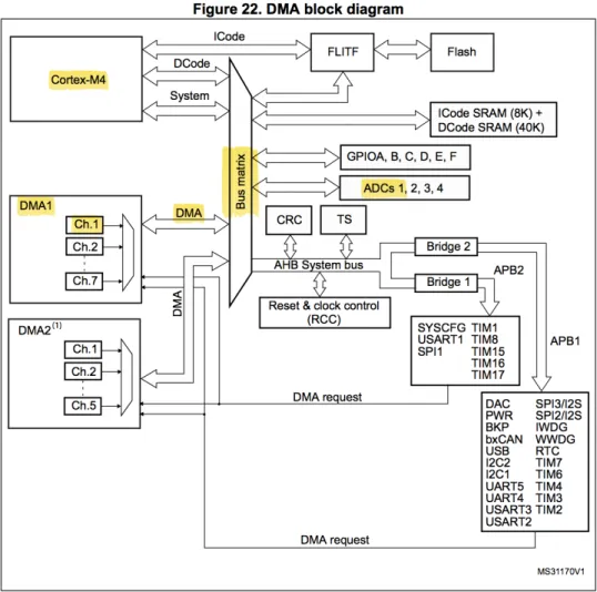
5.6 DMA Register Settings
The DMA module allows us to capture large sections of data at a time, and then send them as a stream over USB. There are two DMA
modules in the microcontroller. We are only using DMA1 channel 1 for this oscilloscope system. The signal path follows the yellow sections of Fig 5-11.
Figure 5-11. DMA Block Diagram.
DMA1_CCR1 is the Channel Control Register for DMA1. We select high priority with both the memory and peripheral size as 8-bit (as the ADC is 8-bit). We also must set the memory increment feature
(DMA_CCR_MINC) and the transfer complete IRQ (DMA_CCR_TCIE). DMA1_CNDTR1 dictates the size of the data buffer for one DMA sweep (after which the DMA transfer complete IRQ fires). This controls the size of the sample buffer for one gel.
DMA1_CPAR1 is the Peripheral Address Register for channel 1 of DMA1. This must be set to the address of the ADC data register. Data is taken from this address and placed in the data buffer.
DMA1_CMAR1 is the memory address register for channel 1 DMA1. This must be set to the address of the data buffer.
Lastly, we must enable the DMA NVIC interrupt, which will go high whenever a sample buffer is filled. We must also enable the DMA module after the register settings have been completed.
5.6.1 DMA – ADC Module
If all the ADC and DMA settings are correct, the system should behave as described in Fig 5-12.
Similarly to Fig 5-2, the trigger activates the timer that then initiates the ADC. The DMA and the ADC have a feedback loop that completes once the memory buffer for data is full. This then generates the DMA transfer complete IRQ. If all 8 gels of data are collected, the data buffer will be sent through USB, otherwise the phase increments and the trigger is re-armed to capture another gel of data.
Figure 5-12. Flow chart for ADC-DMA subsystem.
5.6.2 USB
The USB library employed is native to libopencm3. There are two primary functions: cdcacm_data_tx_cb and cdcacm_data_rx_cb. The cdcacm_data_tx_cb function is called whenever the usbd_ep_write_packet function is called. Likewise, the cdcacm_data_rx_cb function is called whenever the usbd_ep_read_packet function is called (essentially whenever the laptop sends data).
5.6.3 Summary
In short, the four main firmware pieces of this system are the timer, ADC, DMA, and USB. Together all contribute to the sequential sampling system with phase increments. Careful register settings must be executed for the hardware modules on the microcontroller.
6 Signal Processing
The input signal is processed in MATLAB and displayed as a graphical figure.
6.1 Signal Chain
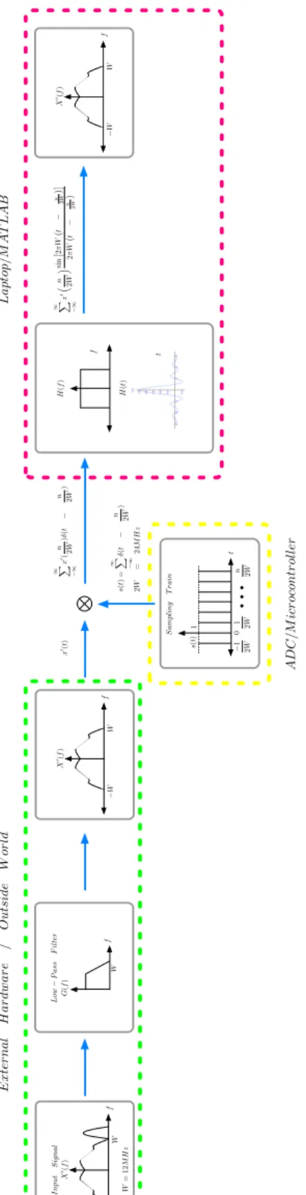
Ideally the signal chain should appear as in Fig 6-1. There are three main sections: 1) the pre-filtered analog signal and input filtering hardware (green), 2) the sampling from the ADC of the STM32F3 (yellow), 3) the reconstruction in MATLAB (pink).
Ideally, the input signal would be filtered by a low-pass filter with a ½ LSB magnitude at the cutoff of 12MHz (Fig 6-1 green-dashed box). The low-passed input would then be sampled by the STM32F3 (modeled as a delta train of 24MHz in the yellow-dashed box of Fig 6-1).
The input signal and the delta train would then produce a series of copies in the frequency domain (Fig 6-2). A brick wall in the frequency domain would afterwards process this train of copied signals; we would return our original low-pass filtered signal (Fig 6-1, pink-dashed box).
Figure 6-1. Frequency domain description of process. x 0(t) Low P a ss F il te r W G (f ) f s( t)= 1X 1 (t n 2W ) 2 W = 24 MH z H (f ) H (t ) X 0(f) f W W In p u t S ig n a l f W X 0(f ) W W = 12 MH z 1X 1 x 0( n)2W (t n 2W ) S a mp li n g T ra in t n 2W 1 2W 0 1 2W s( t) f t 1X 1 x 0 ⇣ n 2W ⌘sin ⇥ 2⇡ W t n2W ⇤ 2 ⇡ W t n2W f W X 0(f ) W AD C /M ic ro co n tr ol le r L a p to p /M AT L AB Ex te rn a l H a rd w a re / O u ts id e W or ld 1
Figure 6-2
A few liberties were taken with this ideal signal chain. The input low-pass filter was somewhat omitted. The input amplifier of our scope provides some inherent filtering to 16MHz. the AD823 op-amp provides 16MHz of bandwidth only for signals of < 0.2Vpp and distorts large amplitude signals as a “shark fin” shape (Fig 6-3).
Figure 6-3. 2Vpp sine input at 4MHz.
One hopes all input signals transmitted to the scope are less than 12MHz. This may be somewhat problematic for signals such as triangle or square waves, for their Fourier coefficients continue infinitely. Such waveforms would result in high-order coefficients aliasing onto our input
W f X0(f ) W 2W⇤ X0(0) 3W 2W 0 2W 3W nW nW (n + 2)W (n + 2)W TP2 TP2+1.5V TP1
waveform. This would manifest as distortion in lower frequency bands if these coefficients were not of small enough amplitude.
Another problem is clock jitter. If the clock is jittery, our samples will contain artifacts, particularly for high frequency input signals. Future characterizations must be performed to minimize this effect. A GPIO pin can be connected to the ADC-DMA clock to measure the clock frequency precision, however one must be aware of the clock cycles necessary to push the GPIO command.
In addition, the 24MHz sampling is approximated through
sequential sampling as 8 gels of 3MSPS. We must not forget we technically only have a 3MSPS ADC and noise may be picked up cyclically during sequential sampling.
6.2 MATLAB Reconstruction
In order to reconstruct our signal, we pass our raw input data through MATLAB code. This code can later be imported to Python so as to be free for potential students and users.
6.2.1 MATLAB Code Overview
The MATLAB code must do two things: 1) parse the data packet into separate components, 2) perform signal reconstruction on these components.
6.2.1.1 Data Packet
The data packet sent by the STM32F3 contains all eight gels of phase information and a beginning packet with eight sampled values of the trigger voltage. Within the microcontroller, the USB send function
(usbd_ep_write_packet) transmits a buffer of 65 characters. We have chosen to use 62 characters in case future modifications require identifying the buffer. We then have 75 sets of 62 characters per gel (Fig 6-4). Hence, the total number of 8-bit samples per gel is 4650.
Figure 6-4. Data Packet Structure. Da ta P a ck et Tr ig g er S a mp le s Ze ro Gel 0 Gel 1 Gel 2 Gel 3 Gel 4 Gel 5 Gel 6 Gel 7 [1 : 8] [9 : 61] [0] Ze ro s [62 : 4711] [4712 : 9361] [9362 : 14011] [14012 : 18661] [18662 : 23311] [23312 : 27961] [27962 : 32611] [32612 : 37261] (Gel 0) [0] (Gel 1) [0] (Gel 2) [0] (Gel 3) [0] (Gel 4) [0] (Gel 5) [0] (Gel 6) [0] (Gel 7) [0] (Gel 0) [1] (Gel 1) [1] (Gel 2) [1] (Gel 3) [1] (Gel 4) [1] (Gel 5) [1] (Gel 6) [1] (Gel 7) [1] (Gel 1) [2] (Gel 2) [2] (Gel 3) [2] (Gel 4) [2] Av er a g e( Tr ig g er S a mp le s[ 1 : 8] ) Amp li tu d e S a mp le s Gel 1[ 0] ,G el 2[ 0] ,G el 3[ 0] ,G el 4[ 0] ,G el 5[ 0] ,G el 6[ 0] ,G el 7[ 0] Gel 1[ 1] ,G el 2[ 1] ,G el 3[ 1] ,G el 4[ 1] ,G el 5[ 1] ,G el 6[ 1] ,G el 7[ 1] Gel 1[ 2] ,G el 2[ 2] ,G el 3[ 2] ,G el 4[ 2] ... In d ex ”0” of al l g el s. In d ex ”1” of al l g el s. In d ex ”2” of al l g el s.
After the data packet is decoded, we then re-order the gels to obtain the 24MHz-sampled waveform. Each gel packet is of length 4650. To construct the waveform, we first take all index “0”s of each gel (gel0[0], gel1[0],…gel7[0]). These samples become the first 8 samples of the 24MHz-sampled signal. To obtain the next eight samples we use gel0[1], gel1[1],…gel7[1], and to acquire the next eight, we use gel0[2],
gel1[2],…gel7[2], and so on and so forth to gel0[4649], gel1[4649],…gel7[4649].
In the re-ordered sine wave in Fig 6-4, we see how sections from each gel (labeled by its color) are then re-ordered. The first rainbow set of samples is index 0 of the eight gels from the data packet. The next rainbow set is index 1 of the eight gels from the data packet. The next rainbow set is index 2 of the eight gels from the data packet. This continues until index 4649 of all eight gels.
6.2.1.1.1 Fast Fourier Transform
To obtain the frequency decomposition of the input signal, we employ a Fast Fourier Transform (FFT) to attain the values of relevant frequency coefficients.
MATLAB’s fft(X,n) command returns the n-point Discrete Fourier Transform of the input vector X. A word of caution – this process is
inherently a circular convolution. If performed carelessly, the input signal is presumed infinite in time and repetitious in waveform, which may lead to distortion. A filtering window such as Hanning should be used beforehand on the signal. For this project, it was not and there are artifacts from this omission.
One point of interest is that this FFT function must later be implemented in Python.
6.2.1.1.2 Sinc Interpolation
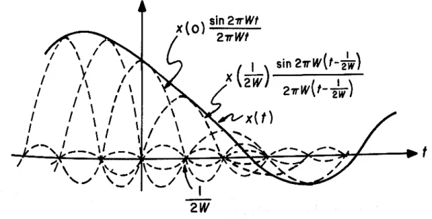
Our primary reconstruction method derives from the Nyquist-Shannon Sampling Theorem:
“Suppose that 𝑿(𝒇), the Fourier transform of 𝒙(𝒕), is identically zero for all 𝒇 > 𝑾 and has no singularities at 𝒇 = 𝑾. Then 𝒙(𝒕) has exactly the representation: 𝒙 𝒕 = 𝒙 𝒏 𝟐𝑾 ! 𝒏! !! 𝐬𝐢 𝐧 𝟐𝝅𝑾 𝒕 − 𝟐𝑾𝒏 𝟐𝝅𝑾 𝒕 − 𝒏𝟐𝑾 Equation 2
That is, samples of 𝒙(𝒕) at points 𝒕 = 𝟐𝑾𝒏 (samples that are 𝟐𝑾𝟏 apart in time) completely determine 𝒙(𝒕) at all points in time” [10].
Figure 6-5, William Siebert, Circuits, Signals, and Systems. Cambridge, MA, USA: The MIT Press, 1986. [10]
One should recognize that this sinc-interpolation method (Fig 6-5) is the time-domain representation of filtering the sampled input signal with an ideal frequency domain brick-wall (pink dashed box in Fig 6-1).
From this, it is possible to reconstruct a continuous signal from a discretized signal. However, the interpolation summation limits would then have to be infinite. This is too time-consuming, so we must be cautious with the selection of our summation limits.
The sinc-interpolation function used, 𝐲 = 𝐬𝐢𝐧𝐜_𝐢𝐧𝐭𝐞𝐫𝐩(𝐱, 𝐬, 𝐮), is credited to Ted Pavlic [11]. A Python version exists as well [12]. In this interpolation function, the inputs are: "𝐬” – a vector of the input signal length spaced 1/24MHz apart, and “𝐮” – a vector of the desired up-sampled time steps (for example a vector of 1/48MHz spaced apart time steps). The input vector, 𝐱, is then remapped to the higher frequency time samples while simultaneously sinc-interpolated. Connecting back to Equation 2, the original input time step vector controls 𝒏 and the desired up-sampled time step vector controls 𝒕. 𝒙 𝟐𝑾𝒏 is the input vector 𝐱, and our output 𝐲 is 𝒙 𝒕 .
This function takes considerably less time than attempting to brute force Equation 2.
Important to note, this function is a finite element method procedure rather than a circular convolution procedure. A brick wall filter is often implemented through the relationship of convolution and multiplication in the frequency domain.
𝒙 ∗ 𝒚 = 𝑭!𝟏 𝑭(𝒙) ∙ 𝑭(𝒚)
Equation 3
In a typical circular convolution approach, we would FFT our input and our sinc, producing a Fourier transformation of our signal and a brick wall. We would then multiply the two and inverse FFT (IFFT) the product.
In one sense, this is easier to visualize. However, these types of FFT and IFFT procedures are typically performed in MATLAB as circular
convolutions that assume the signal is perpetually periodic in time. Regrettably, our signal is finite. Should we attempt to interpolate with a circular convolution, we would witness the appearance of slow time-domain waveforms that do not physically exist in our signal - Moiré patterns
(explained in later section).
Furthermore, an FIR filter with a sinc kernel does not yield as high of an SNR as finite element sinc-interpolation. A limit exists for the FIR sinc kernel window length – some initial values of the convolution between the input and the sinc-filter must be discarded. If the kernel size is too large, we must reject the majority of our convolution. However, decreasing the sinc kernel length creates a less precise and less smooth output signal due to the fact that unlike interpolation, we do not create a higher sample point density with an FIR filter. While the FIR method is faster, it still exhibits Moiré patterns in our frequency range, even with a large kernel window. Ultimately the finite element method was selected.
6.2.1.2 Signal Reconstruction Overview
The main procedure in MATLAB is outlined in Fig 6-6. The
reconstruction depends on the input waveform shape. Should a user select a sine wave input, the code will specifically hunt for the highest frequency component and interpolate with a frequency window. Should the user select a square or triangle wave, the user should not opt for any pre-conditioning filter (so as to avoid accidental deletion of higher order components).
The reconstruction begins by first averaging the trigger values. The reconstructed signal (the main waveform of Fig 6-4) is then
sinc-interpolated by a factor of two to reduce noise in the sampled signal so that the subsequent FFT can locate the center frequency. Depending on the input signal, the user can either select to window the frequency around the center frequency by 1/8th of the Nyquist frequency (limit the band around
the center frequency to 1.5MHz) or to allow the interpolated signal to be processed without additional frequency windowing. After this, the signal is again sinc-interpolated by a factor of 10 (to smooth out any additional Moiré patterns) and the waveform is displayed with the original trigger value.
Figure 6-6. MATLAB code outline.
Data Reconstruction
T rigger V alue Discrete W avef orm
W avef orm Shape
Sine W ave
Y es N o
F F T Data P acket[1 : 8] Data P acket[62 : 37261]
Sinc Interpolate F actor of 2fs
W indow around center f requency by 1 8 of 1st N yquist Band Sinc Interpolate F actor of 10fs Sinc Interpolate F actor of 10fs Display Display
6.2.1.3 Signal Reconstruction Issues
There were a few unexpected issues with the signal reconstruction mainly due to Moiré patterns. Particular waveforms, such as square waves and triangles, present obstacles due to the higher frequency components aliasing into lower bands.
6.2.1.3.1 Moiré Patterns
During the digitization process, a pseudo-aliasing phenomenon called the Moiré effect occasionally occurs [13]. This effect emerges within the first Nyquist band and appears as a slow envelope atop the input signal (Fig 6-7).
Figure 6-7. Moiré Patterning.
The waveforms in Fig 6-6 are MATLAB simulations of an input signal captured within first Nyquist. The original input signal is green and the discretized signal is blue. The discretized signal is sampled at a rate of
𝒇𝒔𝒊𝒈𝒏𝒂𝒍
discretized sine waveform (bottom graph) displays the highest amplitude coefficient at the correct normalized frequency, (𝟏.𝟔𝟏𝟖)𝟏 = 𝟎. 𝟔𝟏𝟖 of 𝒇𝒔𝒊𝒈𝒏𝒂𝒍
𝟐
with rounded amplitudes for the other coefficients, but the time-domain discretized signal has a slow envelope.
This envelope and FFT shape is not due to external noise or aliasing, rather due to discretization and a lack of sinc-interpolation. The actual input signal is windowed and finite in the time-domain. However, as discussed earlier, when we perform an FFT through circular convolution, we imagine the signal as infinite and repetitious. This allows the Moiré patterns to show, for if the signals were infinite and repetitious, the “slow-envelope” signal energy would average to zero. Additionally, this explains the lack of Fourier coefficients for the envelope in the frequency domain.
6.2.1.4 Signal Reconstruction Later Improvements
In the future, the reconstruction could be optimized for speed and refresh rate. Memory allocation between the microcontroller and user laptop could also be improved. A better input filter could be designed with proper impedance matching. An appropriately designed window (Hanning, Gaussian, etc) would also help the FFT aspect of our signal processing.
7 Data and Specs
7.1 Overall Performance (Input Stage + ARM)
In total, we have an oscilloscope with 24MSPS and a gain pre-amp with various bandwidths and a 2.5 V/µs (very, very conservative estimate) slew rate.
7.1.1 Normal \ Real-Time Mode 7.1.1.1 Signal Path Description
In normal mode, we return a stream of samples from the ADC. No trigger is required. In our software, a small interpolation by a factor of ten is performed. This reduces most Moiré effects. Although one can
theoretically capture waveforms up to 1.5MHz, we advise against this. Tektronix does not use the full bandwidth - only !!
!.! to allow for some sinc
interpolation margin [14]. Thus, we suggest operating in normal mode only up to 1.2MHz.
Keep in mind the number of coefficients necessary to view a
waveform. Should the user attempt interpolating a square or triangle wave in this mode, the user must avoid frequencies above or near 500kHz.
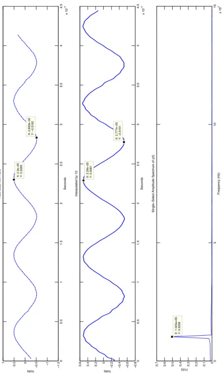
In the following figures, a characterization of normal/real-time mode was performed. Sinusoids of frequencies 100kHz – 1.4MHz were captured with 500mVpp amplitudes (all below 2.5 V/µs slew-rate). As we can see, the 1.4MHz sinusoid displays artifacts. In each figure, the top is the raw data, middle is sinc-interpolated data, bottom is FFT of sinc-interpolated data.
Figure 7-1. 100kHz sine wave. 500mVpp. SNR raw = 33.90dB. SNR interpolated = 37.3dB. 0 0.5 1 1.5 2 2.5 3 3.5 4 4.5 x 10 − 5 − 1.5 − 1 − 0.5 0 0.5 1 X: 2.833e − 05 Y: − 0.5162 Volts X: 2.3e − 05 Y: 0.5065
Raw Data from ADC
Seconds 0 0.5 1 1.5 2 2.5 3 3.5 4 4.5 x 10 − 5 − 0.8 − 0.6 − 0.4 − 0.2 0 0.2 0.4 0.6 X: 2.777e − 05 Y: − 0.5161 X: 2.29e − 05 Y: 0.5081 Interpolated by 10 Seconds Volts 0 5 10 15 x 10 5 0 0.1 0.2 0.3 0.4 0.5 0.6 0.7 X: 1.025e+05 Y: 0.5058 Single −
Sided Amplitude Spectrum of y(t)
Frequency (Hz)
Figure 7-2. 600kHz sine wave 500mVpp. SNR raw = 23.18dB. SNR interpolated = 29.82dB. 0 0.5 1 1.5 2 2.5 3 3.5 4 4.5 x 10 − 5 − 0.4 − 0.3 − 0.2 − 0.1 0 0.1 0.2 0.3 X: 2e − 05 Y: − 0.2313 Volts X: 2.067e − 05 Y: 0.2219
Raw Data from ADC
Seconds 0 0.5 1 1.5 2 2.5 3 3.5 4 4.5 x 10 − 5 − 0.4 − 0.3 − 0.2 − 0.1 0 0.1 0.2 0.3 X: 1.967e − 05 Y: − 0.234 X: 2.05e − 05 Y: 0.2583 Interpolated by 10 Seconds Volts 0 5 10 15 x 10 5 0 0.05 0.1 0.15 0.2 0.25 0.3 0.35 X: 6.006e+05 Y: 0.2515 Single −
Sided Amplitude Spectrum of y(t)
Frequency (Hz)
Figure 7-3. 1.2MHz sine wave 500mVpp. SNR raw = 16.44dB. SNR interpolated = 24.36dB 0 0.5 1 1.5 2 2.5 3 3.5 4 4.5 x 10 − 5 − 0.4 − 0.3 − 0.2 − 0.1 0 0.1 0.2 0.3 X: 2.1e − 05 Y: 0.2431 Volts X: 2.067e − 05 Y: − 0.2449
Raw Data from ADC
Seconds 0 0.5 1 1.5 2 2.5 3 3.5 4 4.5 x 10 − 5 − 0.4 − 0.3 − 0.2 − 0.1 0 0.1 0.2 0.3 X: 2.073e − 05 Y: 0.2586 X: 2.033e − 05 Y: − 0.256 Interpolated by 10 Seconds Volts 0 5 10 15 x 10 5 0 0.05 0.1 0.15 0.2 X: 1.201e+06 Y: 0.1787 Single −
Sided Amplitude Spectrum of y(t)
Frequency (Hz)
Figure 7-4. 1.4MHz sine wave 500mVpp. SNR raw = 15.15dB. SNR interpolated = 22.63dB. 0 0.5 1 1.5 2 2.5 3 3.5 4 4.5 x 10 − 5 − 0.4 − 0.3 − 0.2 − 0.1 0 0.1 0.2 0.3 X: 2e − 05 Y: 0.2548 Volts X: 1.967e − 05 Y: − 0.2565
Raw Data from ADC
Seconds 0 0.5 1 1.5 2 2.5 3 3.5 4 4.5 x 10 − 5 − 0.4 − 0.3 − 0.2 − 0.1 0 0.1 0.2 0.3 X: 1.97e − 05 Y: 0.2548 X: 1.937e − 05 Y: − 0.2565 Interpolated by 10 Seconds Volts 0 5 10 15 x 10 5 0 0.05 0.1 0.15 0.2 X: 1.399e+06 Y: 0.1779 Single −
Sided Amplitude Spectrum of y(t)
Frequency (Hz)
For lower frequency waveforms, the signal captured by the ADC already contains a sufficient sample/point density that there is no significant change in SNR. As we approach higher frequencies (and the point density decreases) we still see a factor of at least 5dB improvement. This reduces the slow envelope in Fig 7-3, but as previously stated, we suggest capturing signals only to 1.2MHz.
The following set of figures is for triangle and square waves
captured in normal mode. Again, in each figure: top is the raw data, middle is sinc-interpolated data, and bottom is FFT of sinc-interpolated data.
Figure 7-5. 100kHz triangle. 500mVpp. 0 0.5 1 1.5 2 2.5 3 3.5 4 4.5 x 10 − 5 − 0.4 − 0.3 − 0.2 − 0.1 0 0.1 0.2 0.3 X: 3.133e − 05 Y: 0.2456 Volts X: 2.633e − 05 Y: − 0.2541
Raw Data from ADC
Seconds 0 0.5 1 1.5 2 2.5 3 3.5 4 4.5 x 10 − 5 − 0.4 − 0.3 − 0.2 − 0.1 0 0.1 0.2 0.3 X: 2.61e − 05 Y: − 0.2516 X: 3.103e − 05 Y: 0.2456 Interpolated by 10 Seconds Volts 0 5 10 15 x 10 5 0 0.05 0.1 0.15 0.2 0.25 X: 1.025e+05 Y: 0.2027 X: 3.076e+05 Y: 0.02295 X: 5.127e+05 Y: 0.006907 Single −
Sided Amplitude Spectrum of y(t)
Frequency (Hz) |Y(f)| X: 7.178e+05 Y: 0.003228 X: 9.155e+05 Y: 0.002064 X: 1.121e+06 Y: 0.001523 X: 1.26e+06 Y: 0.001721
![Figure 2-1. Output signal displays aliasing if input frequency higher than Nyquist cutoff [3]](https://thumb-eu.123doks.com/thumbv2/123doknet/14087753.464315/12.918.241.680.308.600/figure-output-signal-displays-aliasing-frequency-higher-nyquist.webp)