HAL Id: hal-00515076
https://hal.archives-ouvertes.fr/hal-00515076
Submitted on 4 Sep 2010HAL is a multi-disciplinary open access archive for the deposit and dissemination of sci-entific research documents, whether they are pub-lished or not. The documents may come from teaching and research institutions in France or abroad, or from public or private research centers.
L’archive ouverte pluridisciplinaire HAL, est destinée au dépôt et à la diffusion de documents scientifiques de niveau recherche, publiés ou non, émanant des établissements d’enseignement et de recherche français ou étrangers, des laboratoires publics ou privés.
Double-Gate MOSFET-based circuit including
ballistic/quasi-ballistic effects
Sebastien Martinie, Daniela Munteanu, Gilles Le Carval, Jean-Luc Autran
To cite this version:
Sebastien Martinie, Daniela Munteanu, Gilles Le Carval, Jean-Luc Autran. Analytical modelling and performance analysis of Double-Gate MOSFET-based circuit including ballistic/quasi-ballistic effects. Molecular Simulation, Taylor & Francis, 2009, 35 (08), pp.631-637. �10.1080/08927020902769836�. �hal-00515076�
For Peer Review Only
Analytical modelling and performance analysis of Double-Gate MOSFET-based circuit including ballistic/quasi-ballistic
effects
Journal: Molecular Simulation/Journal of Experimental Nanoscience Manuscript ID: GMOS-2008-0204.R1
Journal: Molecular Simulation Date Submitted by the
Author: 18-Dec-2008
Complete List of Authors: martinie, sebastien; CEA-LETI MINATEC; IM2NP-CNRS Munteanu, Daniela; IM2NP-CNRS
Le Carval, Gilles; CEA-LETI MINACTEC Autran, Jean-luc; IM2NP-CNRS
Keywords: Double-Gate MOSFET, ballistic/quasi-ballistic transport , compact model, ring oscillator
For Peer Review Only
1
Reply to Reviewer:
We want to thank the reviewers for their comments and very pertinent suggestions. The manuscript has been revised according to their recommendations as shown in the following.
1) Reviewer’s comment point 1:
Response: We agree with the reviewer comment, there is typographic error in equation (1):
Considering the corresponding signs of in (1-R)/(1+R), we obtain:
+ − + − + − − = − − T k qV T k qV th T GS ox D DS DS e R R e R R v V V C W I . . 1 1 1 1 . 1 1 . ). .( . (1)
2) Reviewer’s comment point 2:
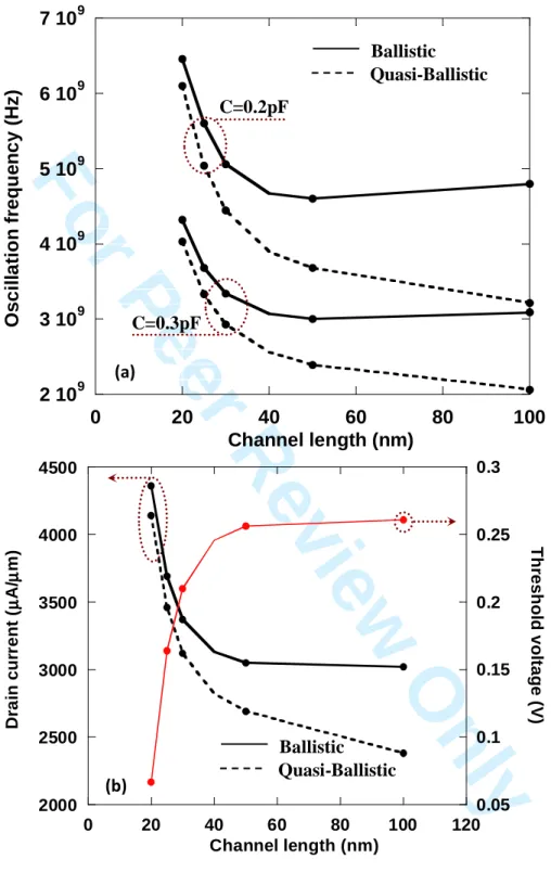
Response: Figure 6.a illustrates the impact of the channel length on the oscillation frequency.
For the smallest length the oscillation frequency increases due to SCE/DIBL. But for long channel case the transport (ballistic or quasi-ballistic) is predominant, thus oscillation frequency decrease in quasi-ballistic case because this depends on the channel length and is constants for ballistic transport as the Ion. But, effectively we suspect that the increase of the
oscillation frequency in the ballistic case is not realistic due to numerical noise in our code. In fact this is not really important for the objective of our study, which is dedicated to the simulation of short length.
3) Reviewer’s comment point 3:
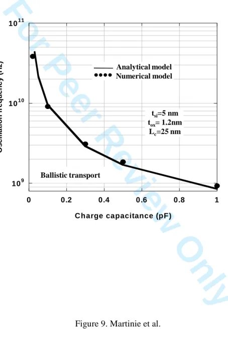
Response: The figure 9 has been corrected to include the structural parameter of the DG
MOSFET: 109 1010 1011 0 0.2 0.4 0.6 0.8 1 O s c il la ti o n f re q u e n c y ( H z ) Charge capacitance (pF) Ballistic transport Analytical model Numerical model tsi=5 nm tox= 1.2nm Lc=25 nm 1 2 3 4 5 6 7 8 9 10 11 12 13 14 15 16 17 18 19 20 21 22 23 24 25 26 27 28 29 30 31 32 33 34 35 36 37 38 39 40 41 42 43 44 45 46 47 48 49 50 51 52 53 54 55 56 57 58 59 60
For Peer Review Only
Analytical modelling and performance analysis
of Double-Gate MOSFET-based circuit
including ballistic/quasi-ballistic effects
S. Martinie*1,2, D. Munteanu2, G. Le Carval1, J.L. Autran2,3
1
CEA-LETI MINATEC, 17 rue des Martyrs, 38054 Grenoble, Cedex 9, France.
2
IM2NP-CNRS, UMR CNRS 6242, Bât. IRPHE, 49 rue Joliot Curie, BP 146, 13384 Marseille Cedex 13, France.
3
University Institute of France (IUF), 75000 Paris, France.
*Corresponding author: Mr. Sébastien MARTINIE CEA-LETI MINATEC, 17 rue des Martyrs,
38054 Grenoble, Cedex 9, France Phone: (33) 4 38 78 18 40 Fax: (33) 4 38 78 51 40 E-mail: [email protected] 1 2 3 4 5 6 7 8 9 10 11 12 13 14 15 16 17 18 19 20 21 22 23 24 25 26 27 28 29 30 31 32 33 34 35 36 37 38 39 40 41 42 43 44 45 46 47 48 49 50 51 52 53 54 55 56 57 58 59 60
For Peer Review Only
ABSTRACT
In this paper we present a compact model of Double-Gate MOSFET architecture including ballistic and quasi-ballistic transport down to 20 nm channel length. In addition, this original model takes into account short channel effects (SCE/DIBL) by a simple analytical approach. The quasi-ballistic transport description is based on Lundstrom’s backscattering coefficient given by the so-called flux method. We also include an original description of scattering of processes by introducing the “dynamical mean free path” formalism. Moreover, we implemented our model in a Verilog-A environment, and applied it to the simulation of circuit elements such as CMOS inverters and Ring Oscillators to analyze the impact of ballistic/quasi-ballistic transport on circuit performances. Finally, in order to validate our work, we confronted this model with numerical simulation of CMOS and Ring Oscillator in ballistic case.
Keywords: Double-Gate MOSFET, ballistic/quasi-ballistic transport, compact model,
Ring Oscillator. 1 2 3 4 5 6 7 8 9 10 11 12 13 14 15 16 17 18 19 20 21 22 23 24 25 26 27 28 29 30 31 32 33 34 35 36 37 38 39 40 41 42 43 44 45 46 47 48 49 50 51 52 53 54 55 56 57 58 59 60
For Peer Review Only
1. Introduction
As the MOSFET continues to shrink rapidly, emerging physical phenomena, such as ballistic transport, have to be considered in the modelling and simulation of ultra-scaled devices. Future Double-Gate MOSFETs (DGMOS Fig. 1), designed with channel lengths in the decananometer scale, are expected to be more ballistic or quasi-ballistic than diffusive. At this level of miniaturisation is essential to directly evaluate the impact of ballistic and quasi-ballistic transport at circuit level through simulation of several circuit demonstrators. The implementation of compact models in Verilog-A (Smartspice [1]) environment offers the opportunity to describe as accurately as possible the physics of transport and to analyze its impact on various circuit elements.
Several analytical models based on the Drift-Diffusion formalism demonstrate that it is possible to introduce the diffusive transport in compact modelling. However, when the channel length approaches the value of mean free path, the mobility definition can no more strictly explain the electronic transport in the device [2]. In this case we use the flux theory and the main parameter of this approach is the backscattering coefficient, which expresses the ballistic and the quasi-ballistic transport. Some well-known works performed by Lundstrom et al [3-5] demonstrate the usefulness of the flux theory in qualitatively describing quasi-ballistic transport in compact modelling.
More recently several works [6-8] proposed some accurate solution to describe transport for nanoscale DG MOSFETs including quantum confinement or the effect of tunneling through the source-drain potential barrier on devices characteristic. But few works [9-10] exposed the influence of ballistic/quasi-ballistic transport on the operation of circuit demonstrator. 1 2 3 4 5 6 7 8 9 10 11 12 13 14 15 16 17 18 19 20 21 22 23 24 25 26 27 28 29 30 31 32 33 34 35 36 37 38 39 40 41 42 43 44 45 46 47 48 49 50 51 52 53 54 55 56 57 58 59 60
For Peer Review Only
In this work we demonstrate the feasibility of a simulation study of ballistic/quasi-ballistic transport at circuit level and we show the impact of this advanced transport on the switch of CMOS inverter and the oscillation frequency of ring oscillator. This paper is organized as follows: the section I explains the model physics and the corresponding assumptions. In part II, we explain our device simulation in ballistic and quasi-ballistic case. The part III highlights the qualitative connection between physics of quasi-ballistic transport and its impact on circuit performance. Finally, we compare our model with numerical simulation in terms of CMOS switch and oscillation frequency.
2.DG MOSFET model
A. Ballistic and quasi-ballistic transport
The proposed analytical model (implemented in Verilog-A environment) is based on the well-known work of Natori [10] and Lundstrom [3]. This formula describes the ballistic and quasi-ballistic current:
+ − + − + − − = − − T k qV T k qV th T GS ox D DS DS e R R e R R v V V C W I . . 1 1 1 1 . 1 1 . ). .( . (1)
where W is the gate width, Cox is the gate oxide capacitance, VGS is the gate to source
voltage, VDS is the drain to source voltage, VT is the threshold voltage, k is the
Boltzmann constant, q is the electron charge and T is the lattice temperature.
In addition, Lundstrom et al. developed physical compact models describing the device operation in quasi-ballistic regimes using the backscattering coefficient R [4]:
λ + = kT kT L L R ; DS c kT V q T k L L . . . = (2)
where λ is the mean free path and LkT is the distance over which the channel potential
drops by kT/q compared to the peak value of the source to channel barrier. Physically,
1 2 3 4 5 6 7 8 9 10 11 12 13 14 15 16 17 18 19 20 21 22 23 24 25 26 27 28 29 30 31 32 33 34 35 36 37 38 39 40 41 42 43 44 45 46 47 48 49 50 51 52 53 54 55 56 57 58 59 60
For Peer Review Only
LkT represents the critical distance over which scattering events modify the current; the limit and the demonstration of the backscattering coefficient are exposed [12].
We consider here the Dynamical mean Free Path which is a “local free path of ballistic carriers” [8]. This characteristic length represents the average distance to be crossed before the next scattering event. This approach considers that each carrier is ballistic as long as any event does not disturb its trajectory. The dynamic mean free path (dfp) connects the ballistic velocity and all interactions (coulomb and acoustic/optical phonon interaction) experienced by carriers crossing the channel. The scattering process with impurities (τimp) and phonon interactions (τph) are calculated as in [8] and the value of
dfp used here is 27 nm in the intrinsic silicon channel. In practice, dfp replaces λ to describe quasi-ballistic transport:
tot bal v dfp= .
τ
; + = = + = − − − DS bal bal bal ph imp tot V q T k m v . . . 2 3 * . 2 1 1 1ε
ε
τ
τ
τ
(3)where m* is the mass in direction of transport, vbal the ballistic velocity, τtot the total
scattering rate and εbal the carrier energy. B. Short channel effects
To obtain an accurate model and describe all electrostatic effects, we have also introduced Short Channel Effect and Drain Induced Barrier Lowering (SCE/DIBL) using the Suzuki’s model [13] for VT. The starting point of this model is the Poisson
equation, where the depleted and the electron charges are neglected:
0 . ) , ( ) , ( 2 2 2 2 ≈ = + Si A N q dy y x d dx y x d
ε
ψ
ψ
(4)Supposing a parabolic dependence in the y-direction:
1 2 3 4 5 6 7 8 9 10 11 12 13 14 15 16 17 18 19 20 21 22 23 24 25 26 27 28 29 30 31 32 33 34 35 36 37 38 39 40 41 42 43 44 45 46 47 48 49 50 51 52 53 54 55 56 57 58 59 60
For Peer Review Only
0 ) ( ) ( 2 2 2 = −λ
η
η
x dx x d (5.a) ox ox Si Si t tε
ε
λ
= . . (5.b)where η=ψs(x)-VGS, ψs(x) is the surface potential, εSi and εox are, respectively, the silicon
and the oxide permittivity. The solution of equation (5.a) is:
+ − = λ λ η λ η η c D c S L sh x sh x L sh x . . ) ( (6)
where the boundary conditions are ηS=ψS(0)-VGS at the source and ηD=ψS(Lc)-VGS at the
drain. ψS(0) is the built-in potential equal to (k.T/q).ln(ND.NA/ni²), ND and NA are,
respectively, the doping level in the source/drain regions and in the channel.
The expression of the threshold voltage shift (∆VT) due to SCE/DIBL depends on the
value of the minimum potential, given by:
λ
η
η
ψ
4. min min( ) 2. . . c L D S GS S x V e − + = (7) − = S D c L xη
η
λ
ln . 2 2 min (8)∆VT is then obtained from the following equation [13]:
λ
η
η
. . 4. . 2 c L D S T e V = − ∆ (9)After some algebraic manipulation, we find the analytical expression of ∆VT. Thus, VT
in equation (1) is modified by ∆VT, as follows:
T th
T V V
V = −∆ (9)
where Vth and ∆VT are the long channel threshold voltage and its variation due to
SCE/DIBL, respectively. 1 2 3 4 5 6 7 8 9 10 11 12 13 14 15 16 17 18 19 20 21 22 23 24 25 26 27 28 29 30 31 32 33 34 35 36 37 38 39 40 41 42 43 44 45 46 47 48 49 50 51 52 53 54 55 56 57 58 59 60
For Peer Review Only
Finally, the above-threshold regime is linked to the subthreshold regime using an interpolation function based on the subthreshold swing S parameter, also defined by Suzuki in [13]: 1 min min( ) ). 10 ln( . . − = GS S dV x d q T k S
ψ
(10)This assures the perfect continuity of our model between on-state regime and off-state regime.
3. Simulation RESULTS
A. Device simulations
After implementation in Verilog-A environment, the model has been used to simulate the DGMOS structure schematically presented in Figure 1. The source and drain regions are heavily doped (1×1020 cm-3) and an intrinsic thin silicon channel is considered. The
channel length varies from 10 nm to 200 nm; a gate oxide of 1.2 nm thick and a midgap metal gate are also considered.
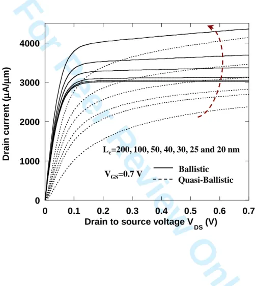
It is well-known that the ballistic current is independent of channel length [11] except when SCE or DIBL appears. In order to clearly confirm this point, simulations have been performed for several length (20, 25, 30, 40, 50, 100 and 200 nm) and considering two types of transport (quasi-ballistic and ballistic; Fig. 2). Note that for the ballistic case, the mean free path value has been chosen to be extremely large compared to the channel length. In contrast to the ballistic case, the quasi-ballistic transport has the same behaviour as that of diffusive transport and the form of the output characteristics depends on Lc.
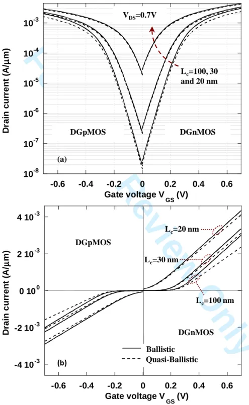
Figure 3 shows the drain current versus the gate voltage characteristics for the DGnMOS and DGpMOS simulated devices at VDS=0.7V. In this approach, we suppose
that the transport description (for ballistic and quasi-ballistic case) for holes is identical to that of electrons, with uniquely changing the thermal velocity value in
non-1 2 3 4 5 6 7 8 9 10 11 12 13 14 15 16 17 18 19 20 21 22 23 24 25 26 27 28 29 30 31 32 33 34 35 36 37 38 39 40 41 42 43 44 45 46 47 48 49 50 51 52 53 54 55 56 57 58 59 60
For Peer Review Only
degenerate conditions (Fig. 1b et 1c, [14]). As expected, the ballistic and quasi-ballistic current shows a perfect continuity between the above and the subthreshold regime (as illustrated on Fig. 3a). Finally, figure 3b shows that the DGnMOS and DGpMOS have the same behaviour in terms of transport, with different current levels due to the different values of thermal velocity.
B. Circuit simulations
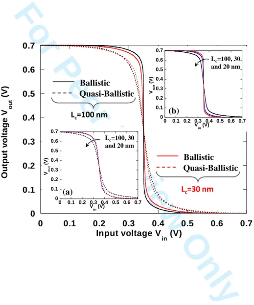
In addition to the simulation of single device operation, we have simulated different circuit elements such as CMOS inverters and ring oscillators (Fig. 1b and 1c) to show the impact of ballistic/quasi-ballistic transport at circuit level.
The output voltage (Vout) of the CMOS inverter switches more sharply from the “1”
state to the “0” state in the ballistic case than in quasi-ballistic transport (Fig. 4). The switch of the CMOS inverter depends on the limit between linear and saturation region, which controls the switch between transistors. When SCE/DIBL occur, the transition between linear and saturate regime is modified, and the switch from the “1” state to the “0” state is less sharp. In the quasi-ballistic case, the abruptness of the CMOS characteristic is strongly deteriorated. In conclusion, these results prove that the ballistic transport improves the switch and the static performances of the CMOS inverter.
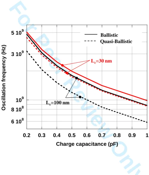
Figure 5 shows the oscillation frequency as a function of the charge capacitance for two channel lengths: 100 and 30 nm. As expected the oscillation frequency is reduced when the charge capacitance increases, due to variation of the propagation time through the inverters. We can also note the strong influence of short channel effects that increase the current value and reduce the difference between the oscillation frequencies in quasi-ballistic transport compared with quasi-ballistic transport.
Moreover, we thoroughly studied the influence of parasitic elements and phenomena on circuit performances. Figure 6.a illustrates the impact of two charge capacitances on the oscillation frequency versus the channel length. Figure 6.b shows the Ion current and VT 1 2 3 4 5 6 7 8 9 10 11 12 13 14 15 16 17 18 19 20 21 22 23 24 25 26 27 28 29 30 31 32 33 34 35 36 37 38 39 40 41 42 43 44 45 46 47 48 49 50 51 52 53 54 55 56 57 58 59 60
For Peer Review Only
versus the channel length. This last figure demonstrates the strong influence of SCE/DIBL effect on the transient performance. The explanation is that when SCE/DIBL effects occur:
- Firstly, the benefit of ballistic transport (versus quasi-ballistic) on the switch of the CMOS inverters is hidden (inset (a) and (b) of Fig. 4).
- Secondly, the Ion current strongly increased (Fig. 6.b).
Consequently the oscillation frequency in ballistic and quasi-ballistic case is less influenced by the value of the dynamic mean free path.
These results show that the oscillation frequency is directly influenced by the type of transport (ballistic versus quasi-ballistic) which changes strongly the static and the transient performances. However, parasitic phenomena such as interconnect capacitances or SCE/DIBL are essential parameters in the analysis of circuit performances even when the intrinsic behaviour of transistors is dominated by ballistic transport.
4. Comparison with numerical Simulation
A. Numerical simulation of ballistic transport using the quasi-ballistic mobility concept
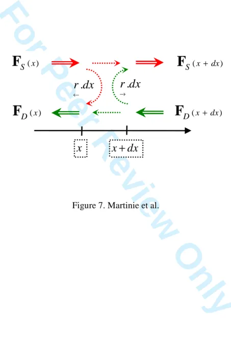
In a previous work we enhanced the pioneering approach of quasi-ballistic mobility proposed by Rhew et al [15] and we introduced it into TCAD simulator, in order to numerically simulate the ballistic/quasi-ballistic transport using a TCAD tool. This approach, extensively presented in [9], is used here to validate our analytical model. In the following, we shortly remind the basic equations of this approach, based on the flux theory or McKelvey’s flux method [2], [15].
Figure 7 shows the schematics of the flux evolution in the channel (in the direction of transport). The two flux densities, FD and FS, incident on a semiconductor slab with
thickness dx, transmit or reflect with the corresponding backscattering probabilities per length r [15]: 1 2 3 4 5 6 7 8 9 10 11 12 13 14 15 16 17 18 19 20 21 22 23 24 25 26 27 28 29 30 31 32 33 34 35 36 37 38 39 40 41 42 43 44 45 46 47 48 49 50 51 52 53 54 55 56 57 58 59 60
For Peer Review Only
) ( ) ( ) ( . . x S x D x D r r dx d F F F ← → − = (11) ) ( ) ( ) ( . . D x S x x S r r dx d F F F ← → − = (12)where r is the scattering probabilities in the presence of an electric field and the symbols “→” and “←” of scattering probabilities represent the carrier’s velocity components that are parallel or anti-parallel, respectively, to the electric field direction. Adding equations (11) and (12) and considering F=FD-FS and n=(FD+FS)/vth (where vth is the
thermal velocity) we obtain:
(
)
0 = − = dx d dx dF FD FS (13) dx dn r r v n v r r r r th th. . . ← → ← → → ← + + + − = F (14)We use here the expression of scattering probabilities proposed in [15] (with the assumption of non-degenerate gas) for the negative charge carrier:
1 − ←r =mfp ; kT x E q mfp r . ) ( . 1 − = − → (15)
where k is the Boltzmann constant, T is the lattice temperature, q is the electron charge, mfp is the mean free path and E is the electric field in the direction of transport. By
analogy to the classical drift-diffusion approach, we obtain the Einstein relation; we define then a new mobility-like parameter, µqb, called quasi-ballistic mobility [7]:
) ( . . 1 . 2 E x q T k mfp vth qb + = µ (16)
This quasi-ballistic mobility is introduced in TCAD software [9] (ATLAS SILVACO [16]). This approach represents an enhanced Drift-Diffusion-like approach to include quasi-ballistic and ballistic effects in the TCAD simulator. The quasi-ballistic mobility model is implemented using an explicit C-interpreter function describing the relation between the mobility and the parallel electric field (equation (16)). All other quantities
1 2 3 4 5 6 7 8 9 10 11 12 13 14 15 16 17 18 19 20 21 22 23 24 25 26 27 28 29 30 31 32 33 34 35 36 37 38 39 40 41 42 43 44 45 46 47 48 49 50 51 52 53 54 55 56 57 58 59 60
For Peer Review Only
(such as the electrostatic potential, electric field, carrier concentration, current densities ...) are computed as usual in TCAD simulation, by solving the Poisson equation coupled to drift-diffusion transport equation. The details and the validation of this approach are explained in [9] and illustrated with simulations of small circuits based on DGMOS technology.
B. Comparison between numerical and analytical simulations
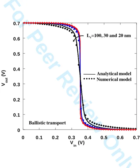
In order to validate the analytical model, we have compared our results with numerical simulation. Figure 8 compares the switch of the CMOS inverter in ballistic case for different channel lengths and illustrates the difference between our analytical model and numerical simulation.
For the long channel case (Lc=100 nm), the ballistic switch for numerical and analytical simulation perfectly matches. But for short channel (Lc=20 nm) a small error is found in
the comparison with numerical data. This is due to the fact that for Lc=20 nm we approach the validity limit of our analytical model (which is Lc=2.tSi in the description of ∆VT). Finally, the numerical simulations confirm the previous remark (exposed in
paragraph 3) that short channel effects deteriorate the switch of the CMOS inverter. Figure 9 compares the analytical and numerical oscillation frequency (for tSi = 5 nm, tox = 1.2 nm, Lc=25 nm) in the ballistic case for different charge capacitances. We note that an identical behaviour is obtained for the numerical and the analytical data, which confirms the result of paragraph 3. Although, a small error exists (error attributed to the Ion value, which is not exactly the same in analytical and numerical case), our analytical
model shows a good agreement with the numerical simulation.
5. Conclusion
In this work, a compact model for DGMOS taking into account ballistic and quasi-ballistic transport has been proposed and implemented in Verilog-A environment. Short channel effects and an interpolation function to link the above and the subthreshold
1 2 3 4 5 6 7 8 9 10 11 12 13 14 15 16 17 18 19 20 21 22 23 24 25 26 27 28 29 30 31 32 33 34 35 36 37 38 39 40 41 42 43 44 45 46 47 48 49 50 51 52 53 54 55 56 57 58 59 60
For Peer Review Only
voltage have been included to obtain a complete description of current characteristics. The dynamical mean free path definition was used to describe scattering processes with impurities and phonons. Finally, the model has been used to simulate two different small-circuits (CMOS inverter and ring oscillators) and to show the significant impact of ballistic/quasi-ballistic transport on the switch of CMOS inverter and the oscillation frequency of ring oscillator. Our simulation results prove that the ballistic transport improves the switch and the static performances of the CMOS inverter, and increases the oscillation frequency of ring oscillators. Finally, we have compared this model with numerical simulation in ballistic case; this comparison also validates our conclusions on the influence of short channel effects and ballistic transport on the operation of circuit elements.
This work also demonstrates the feasibility of a simulation study of ballistic/quasi-ballistic transport at circuit level and highlights the direct relation between the type of transport and static or transient performances of small-circuits.
6. Acknowledgements
This work was supported by the French Ministry of Research (ANR-05-NANO-002 project “MODERN”). The authors would like to acknowledge O. Rozeau, M. Reyboz, V. Barral, T. Poiroux, M-A. Jaud, O Bonno and S. Barraud from CEA-LETI MINATEC (Grenoble, France) for helpful discussions.
1 2 3 4 5 6 7 8 9 10 11 12 13 14 15 16 17 18 19 20 21 22 23 24 25 26 27 28 29 30 31 32 33 34 35 36 37 38 39 40 41 42 43 44 45 46 47 48 49 50 51 52 53 54 55 56 57 58 59 60
For Peer Review Only
References
[1]. SmartSpice Users Manual, SILVACO.
[2]. J.P.McKelvey and J.C. Balogh, “Flux method for the analysis of transport problems in semiconductors in the presence of electric fields”, Phys. Rev., vol 137
no A5, pp. A1555-A1561, Mar. 1965.
[3]. M. Lundstrom and Z. Ren, “Essential physics of carrier transport in nanoscale MOSFETs”, IEEE Trans. Electron Devices,vol. 49, no. 1, pp. 131-141, Jan. 2002.
[4]. M. Lundstrom, “Elementary scattering theory of the Si MOSFET”, IEEE Trans. Electron Device Lett., vol. 18, no 7,pp. 361-363, Jul. 1997.
[5]. A. Rahman and M. S. Lundstrom, “A compact scattering model for the nanoscale double gate MOSFET,” IEEE Trans. Electron Devices, vol. 49, no. 3, pp. 481–489, Mar. 2002.
[6]. J. L. Autran, D. Munteanu, O. Tintori, E. Decarre and A. M. Ionescu, “An analytical subthreshold current model for ballistic quantum-wire double gate MOS transistors”, Molecular Simulation, vol. 31, no. 2/3, pp. 179–183, Feb. 15, 2005.
[7]. D. Munteanu, J.L. Autran, S. Harrison, K. Nehari, O. Tintori and T. Skotniki, “Compact model of the quantum short-channel threshold voltage in symmetric Double-Gate MOSFET”, Molecular simulation, vol. 31, no 12, pp. 831-837, Oct.
2005.
[8]. E. Fuchs, P. Dollfus, S. Barraud, D. Villanueva, F. Salvetti and T. Skotniki, “A new bascattering model giving a description of the quasi-ballistic transport in Nano-MOSFET”, IEEE Trans. Electron Devices, vol. 52, no. 10, pp. 2280-2289,
Oct. 2005.
[9]. S. Martinie, G. Le Carval, D. Munteanu and J.L. Autran, “Impact of ballistic transport on performances of Double-Gate MOSFETs-based circuits”, IEEE Transactions on Electron Devices, vol. 55, no. 9, pp. 2443-2453, Sept. 2008. 1 2 3 4 5 6 7 8 9 10 11 12 13 14 15 16 17 18 19 20 21 22 23 24 25 26 27 28 29 30 31 32 33 34 35 36 37 38 39 40 41 42 43 44 45 46 47 48 49 50 51 52 53 54 55 56 57 58 59 60
For Peer Review Only
[10]. S. Martinie, D. Munteanu, G. Le Carval, J.L. Autran, “A simple compact model to analyze the impact of ballistic and quasi-ballistic transport on ring oscillator performance”, in Proc. Integrated Circuit Design and Technology Conference (IcIcDt), pp. 273-276, Grenoble, France, June 2008.
[11]. K. Natori, “Ballistic metal-oxide-semiconductor field effect transistor “, J. Appl. Phys., vol. 76, no. 8, pp. 4879-4890, Oct. 1994.
[12]. S. Martinie, D. Munteanu, G. Le Carval, J.L. Autran, “New unified analytical model of backscattering coefficient from low to high field conditions in quasi-ballistic transport”, IEEE Electron Device Letters, in press, 2008.
[13]. K. Suzuki, Y. Tosaka and T. Sugii, “Analytical threshold voltage for short channel n+-p+ double-gate SOI MOSFETs”, IEEE Trans. Electron Devices,vol.
43, no. 5, pp. 732-738, May 1996.
[14]. F.Assad, Z. Ren, S. Datta, M. Lundstrom and P. Bendix, “Performance limits of silicon MOSFET’s“, IEEE IEDM Tech. Dig, 1999.
[15]. J-H. Rhew and M. S. Lundstrom, “Drift-diffusion equation for ballistic transport in nanoscale metal-oxide-semiconductor field effects transistor”, J. Appl. Phys.,
vol. 92, no. 9, pp. 5196-5202, Nov. 2002. [16]. ATLAS Users Manual, SILVACO.
1 2 3 4 5 6 7 8 9 10 11 12 13 14 15 16 17 18 19 20 21 22 23 24 25 26 27 28 29 30 31 32 33 34 35 36 37 38 39 40 41 42 43 44 45 46 47 48 49 50 51 52 53 54 55 56 57 58 59 60
For Peer Review Only
Figure captions
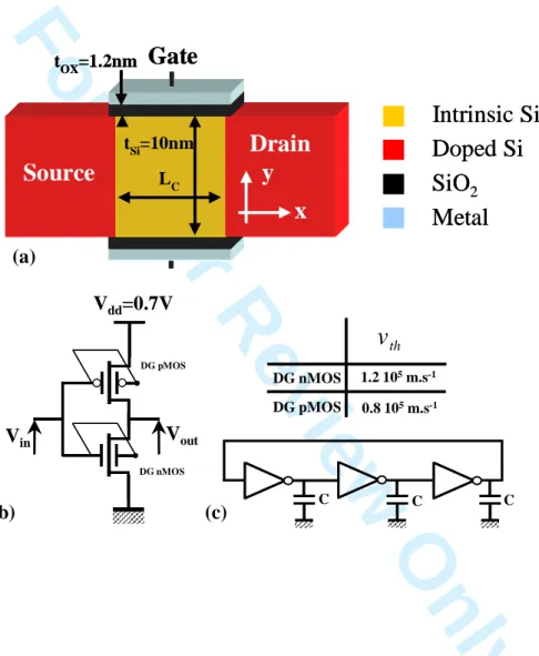
Figure 1. Double-Gate MOSFET (a), CMOS inverter (b), ring oscillator (c) and definition of the main geometrical and electrical parameters.
Figure 2. Drain current versus VDS for Lc=200, 100, 50, 40, 30, 25 and 20 nm and
VGS=0.7 V.
Figure 3. Drain current ((a) log and (b) lin scale) versus VGS for Lc=100, 30 and 20 nm.
Solid line for ballistic transport and dashed line for quasi-ballistic transport.
Figure 4. Vout versus Vin in a CMOS inverter. [Inset (a) and (b): transfer curve in
ballistic and quasi-ballistic case for Lc=100, 30 and 20 nm].
Figure 5. Oscillation frequency versus the charge capacitance for Lc=100 and 30nm
Figure 6. (a) Oscillation frequency versus the channel length for C=0.2 and 0.3 pF. (b) Drain current at VDS=VGS=0.7 V and threshold voltage versus the channel
Figure 7. Description of the flux method parameters.
Figure 8. Vout versus Vin in a CMOS inverter for tSi = 5 nm and tox = 1.2 nm.
Comparison between numerical simulation (diamond) and our analytical model (solid line). 1 2 3 4 5 6 7 8 9 10 11 12 13 14 15 16 17 18 19 20 21 22 23 24 25 26 27 28 29 30 31 32 33 34 35 36 37 38 39 40 41 42 43 44 45 46 47 48 49 50 51 52 53 54 55 56 57 58 59 60
For Peer Review Only
Figure 9. Oscillation frequency versus charge capacitance for tSi = 5 nm, tox = 1.2 nm,
Lc=25 nm. Comparison between our analytical model (solid line) and numerical
simulation [9] (circle). 1 2 3 4 5 6 7 8 9 10 11 12 13 14 15 16 17 18 19 20 21 22 23 24 25 26 27 28 29 30 31 32 33 34 35 36 37 38 39 40 41 42 43 44 45 46 47 48 49 50 51 52 53 54 55 56 57 58 59 60
For Peer Review Only
Figure 1. Martinie et al.
Intrinsic Si
Doped Si
SiO
2Metal
LC tSi=10nm tOX=1.2nmGate
Source
Drain
x
y
Intrinsic Si
Doped Si
SiO
2Metal
LC tSi=10nm tOX=1.2nmGate
Source
Drain
x
y
(a) Vin 1.2 105m.s-1 DG pMOS DG nMOS thv
0.8 105m.s-1 Vout DG pMOS DG nMOS Vdd=0.7V C C C (b) (c) 1 2 3 4 5 6 7 8 9 10 11 12 13 14 15 16 17 18 19 20 21 22 23 24 25 26 27 28 29 30 31 32 33 34 35 36 37 38 39 40 41 42 43 44 45 46 47 48 49 50 51 52 53 54 55 56 57 58 59 60For Peer Review Only
Figure 2. Martinie et al. 0 1000 2000 3000 4000 0 0.1 0.2 0.3 0.4 0.5 0.6 0.7 D ra in c u rr e n t ( µµµµ A / µµµµ m )
Drain to source voltage V
DS (V) Ballistic Quasi-Ballistic VGS=0.7 V Lc=200, 100, 50, 40, 30, 25 and 20 nm 1 2 3 4 5 6 7 8 9 10 11 12 13 14 15 16 17 18 19 20 21 22 23 24 25 26 27 28 29 30 31 32 33 34 35 36 37 38 39 40 41 42 43 44 45 46 47 48 49 50 51 52 53 54 55 56 57 58 59 60
For Peer Review Only
Figure 3. Martinie et al. -4 10-3 -2 10-3 0 100 2 10-3 4 10-3 -0.6 -0.4 -0.2 0 0.2 0.4 0.6 D ra in c u rr e n t (A / µµµµ m ) Gate voltage V GS (V) 10-8 10-7 10-6 10-5 10-4 10-3 -0.6 -0.4 -0.2 0 0.2 0.4 0.6 D ra in c u rr e n t (A / µµµµ m ) Gate voltage V GS (V) (b) (a) Lc=20 nm Lc=30 nm DGpMOS DGnMOS VDS=0.7V DGpMOS DGnMOS Lc=100, 30 and 20 nm Lc=100 nm Ballistic Quasi-Ballistic 1 2 3 4 5 6 7 8 9 10 11 12 13 14 15 16 17 18 19 20 21 22 23 24 25 26 27 28 29 30 31 32 33 34 35 36 37 38 39 40 41 42 43 44 45 46 47 48 49 50 51 52 53 54 55 56 57 58 59 60
For Peer Review Only
Figure 4. Martinie et al. 0 0.1 0.2 0.3 0.4 0.5 0.6 0.7 0 0.1 0.2 0.3 0.4 0.5 0.6 0.7 O u tp u t v o lt a g e V o u t ( V ) Input voltage V in (V) Ballistic Quasi-Ballistic Lc=100 nm Lc=30 nm 0 0.1 0.2 0.3 0.4 0.5 0.6 0.7 0 0.1 0.2 0.3 0.4 0.5 0.6 0.7 V in (V) Vo u t ( V ) 0 0.1 0.2 0.3 0.4 0.5 0.6 0.7 0 0.1 0.2 0.3 0.4 0.5 0.6 0.7 V in (V) V o u t ( V ) Ballistic Quasi-Ballistic Lc=100, 30 and 20 nm Lc=100, 30 and 20 nm (a) (b) 1 2 3 4 5 6 7 8 9 10 11 12 13 14 15 16 17 18 19 20 21 22 23 24 25 26 27 28 29 30 31 32 33 34 35 36 37 38 39 40 41 42 43 44 45 46 47 48 49 50 51 52 53 54 55 56 57 58 59 60
For Peer Review Only
Figure 5. Martinie et al.
6 108 8 108 109 3 109 5 109 0.2 0.3 0.4 0.5 0.6 0.7 0.8 0.9 1 O s c il la ti o n f re q u e n c y ( H z ) Charge capacitance (pF) Lc=100 nm Lc=30 nm Ballistic Quasi-Ballistic 1 2 3 4 5 6 7 8 9 10 11 12 13 14 15 16 17 18 19 20 21 22 23 24 25 26 27 28 29 30 31 32 33 34 35 36 37 38 39 40 41 42 43 44 45 46 47 48 49 50 51 52 53 54 55 56 57 58 59 60
For Peer Review Only
Figure 6. Martinie et al. 2 109 3 109 4 109 5 109 6 109 7 109 0 20 40 60 80 100 O sc il la ti o n f re q u e n c y ( H z ) Channel length (nm) C=0.3pF C=0.2pF Ballistic Quasi-Ballistic 2000 2500 3000 3500 4000 4500 0.05 0.1 0.15 0.2 0.25 0.3 0 20 40 60 80 100 120 D ra in c u rr e n t ( µµµµ A / µµµµ m ) Th re s h o ld v o lt a g e ( V ) Channel length (nm) Ballistic Quasi-Ballistic (b) (a) 1 2 3 4 5 6 7 8 9 10 11 12 13 14 15 16 17 18 19 20 21 22 23 24 25 26 27 28 29 30 31 32 33 34 35 36 37 38 39 40 41 42 43 44 45 46 47 48 49 50 51 52 53 54 55 56 57 58 59 60
For Peer Review Only
Figure 7. Martinie et al. ( )x D
F
( )x SF
F
S (x + dx) (x dx) D +F
dx
r .
→dx
r .
←x
x
+
dx
1 2 3 4 5 6 7 8 9 10 11 12 13 14 15 16 17 18 19 20 21 22 23 24 25 26 27 28 29 30 31 32 33 34 35 36 37 38 39 40 41 42 43 44 45 46 47 48 49 50 51 52 53 54 55 56 57 58 59 60For Peer Review Only
Figure 8. Martinie et al.
0 0.1 0.2 0.3 0.4 0.5 0.6 0.7 0 0.1 0.2 0.3 0.4 0.5 0.6 0.7 V o u t ( V ) V in (V) Ballistic transport Analytical model Numerical model Lc=100, 30 and 20 nm 1 2 3 4 5 6 7 8 9 10 11 12 13 14 15 16 17 18 19 20 21 22 23 24 25 26 27 28 29 30 31 32 33 34 35 36 37 38 39 40 41 42 43 44 45 46 47 48 49 50 51 52 53 54 55 56 57 58 59 60
For Peer Review Only
Figure 9. Martinie et al.
109 1010 1011 0 0.2 0.4 0.6 0.8 1 O s c il la ti o n f re q u e n c y ( H z ) Charge capacitance (pF) Ballistic transport Analytical model Numerical model tsi=5 nm tox= 1.2nm Lc=25 nm 1 2 3 4 5 6 7 8 9 10 11 12 13 14 15 16 17 18 19 20 21 22 23 24 25 26 27 28 29 30 31 32 33 34 35 36 37 38 39 40 41 42 43 44 45 46 47 48 49 50 51 52 53 54 55 56 57 58 59 60
For Peer Review Only
Analytical modelling and performance analysis
of Double-Gate MOSFET-based circuit
including ballistic/quasi-ballistic effects
S. Martinie*1,2, D. Munteanu2, G. Le Carval1, J.L. Autran2,3
1
CEA-LETI MINATEC, 17 rue des Martyrs, 38054 Grenoble, Cedex 9, France.
2
IM2NP-CNRS, UMR CNRS 6242, Bât. IRPHE, 49 rue Joliot Curie, BP 146, 13384 Marseille Cedex 13, France.
3
University Institute of France (IUF), 75000 Paris, France.
*Corresponding author: Mr. Sébastien MARTINIE CEA-LETI MINATEC, 17 rue des Martyrs,
38054 Grenoble, Cedex 9, France Phone: (33) 4 38 78 18 40 Fax: (33) 4 38 78 51 40 E-mail: [email protected] 1 2 3 4 5 6 7 8 9 10 11 12 13 14 15 16 17 18 19 20 21 22 23 24 25 26 27 28 29 30 31 32 33 34 35 36 37 38 39 40 41 42 43 44 45 46 47 48 49 50 51 52 53 54 55 56 57 58 59 60
For Peer Review Only
ABSTRACT
In this paper we present a compact model of Double-Gate MOSFET architecture including ballistic and quasi-ballistic transport down to 20 nm channel length. In addition, this original model takes into account short channel effects (SCE/DIBL) by a simple analytical approach. The quasi-ballistic transport description is based on Lundstrom’s backscattering coefficient given by the so-called flux method. We also include an original description of scattering of processes by introducing the “dynamical mean free path” formalism. Moreover, we implemented our model in a Verilog-A environment, and applied it to the simulation of circuit elements such as CMOS inverters and Ring Oscillators to analyze the impact of ballistic/quasi-ballistic transport on circuit performances. Finally, in order to validate our work, we confronted this model with numerical simulation of CMOS and Ring Oscillator in ballistic case.
Keywords: Double-Gate MOSFET, ballistic/quasi-ballistic transport, compact model,
Ring Oscillator. 1 2 3 4 5 6 7 8 9 10 11 12 13 14 15 16 17 18 19 20 21 22 23 24 25 26 27 28 29 30 31 32 33 34 35 36 37 38 39 40 41 42 43 44 45 46 47 48 49 50 51 52 53 54 55 56 57 58 59 60
For Peer Review Only
1. Introduction
As the MOSFET continues to shrink rapidly, emerging physical phenomena, such as ballistic transport, have to be considered in the modelling and simulation of ultra-scaled devices. Future Double-Gate MOSFETs (DGMOS Fig. 1), designed with channel lengths in the decananometer scale, are expected to be more ballistic or quasi-ballistic than diffusive. At this level of miniaturisation is essential to directly evaluate the impact of ballistic and quasi-ballistic transport at circuit level through simulation of several circuit demonstrators. The implementation of compact models in Verilog-A (Smartspice [1]) environment offers the opportunity to describe as accurately as possible the physics of transport and to analyze its impact on various circuit elements.
Several analytical models based on the Drift-Diffusion formalism demonstrate that it is possible to introduce the diffusive transport in compact modelling. However, when the channel length approaches the value of mean free path, the mobility definition can no more strictly explain the electronic transport in the device [2]. In this case we use the flux theory and the main parameter of this approach is the backscattering coefficient, which expresses the ballistic and the quasi-ballistic transport. Some well-known works performed by Lundstrom et al [3-5] demonstrate the usefulness of the flux theory in qualitatively describing quasi-ballistic transport in compact modelling.
More recently several works [6-8] proposed some accurate solution to describe transport for nanoscale DG MOSFETs including quantum confinement or the effect of tunneling through the source-drain potential barrier on devices characteristic. But few works [9-10] exposed the influence of ballistic/quasi-ballistic transport on the operation of circuit demonstrator. 1 2 3 4 5 6 7 8 9 10 11 12 13 14 15 16 17 18 19 20 21 22 23 24 25 26 27 28 29 30 31 32 33 34 35 36 37 38 39 40 41 42 43 44 45 46 47 48 49 50 51 52 53 54 55 56 57 58 59 60
For Peer Review Only
In this work we demonstrate the feasibility of a simulation study of ballistic/quasi-ballistic transport at circuit level and we show the impact of this advanced transport on the switch of CMOS inverter and the oscillation frequency of ring oscillator. This paper is organized as follows: the section I explains the model physics and the corresponding assumptions. In part II, we explain our device simulation in ballistic and quasi-ballistic case. The part III highlights the qualitative connection between physics of quasi-ballistic transport and its impact on circuit performance. Finally, we compare our model with numerical simulation in terms of CMOS switch and oscillation frequency.
2.DG MOSFET model
A. Ballistic and quasi-ballistic transport
The proposed analytical model (implemented in Verilog-A environment) is based on the well-known work of Natori [10] and Lundstrom [3]. This formula describes the ballistic and quasi-ballistic current:
+ − + − + − − = − − T k qV T k qV th T GS ox D DS DS e R R e R R v V V C W I . . 1 1 1 1 . 1 1 . ). .( . (1)
where W is the gate width, Cox is the gate oxide capacitance, VGS is the gate to source
voltage, VDS is the drain to source voltage, VT is the threshold voltage, k is the
Boltzmann constant, q is the electron charge and T is the lattice temperature.
In addition, Lundstrom et al. developed physical compact models describing the device operation in quasi-ballistic regimes using the backscattering coefficient R [4]:
λ + = kT kT L L R ; DS c kT V q T k L L . . . = (2)
where λ is the mean free path and LkT is the distance over which the channel potential
drops by kT/q compared to the peak value of the source to channel barrier. Physically,
1 2 3 4 5 6 7 8 9 10 11 12 13 14 15 16 17 18 19 20 21 22 23 24 25 26 27 28 29 30 31 32 33 34 35 36 37 38 39 40 41 42 43 44 45 46 47 48 49 50 51 52 53 54 55 56 57 58 59 60
For Peer Review Only
LkT represents the critical distance over which scattering events modify the current; the limit and the demonstration of the backscattering coefficient are exposed [12].
We consider here the Dynamical mean Free Path which is a “local free path of ballistic carriers” [8]. This characteristic length represents the average distance to be crossed before the next scattering event. This approach considers that each carrier is ballistic as long as any event does not disturb its trajectory. The dynamic mean free path (dfp) connects the ballistic velocity and all interactions (coulomb and acoustic/optical phonon interaction) experienced by carriers crossing the channel. The scattering process with impurities (τimp) and phonon interactions (τph) are calculated as in [8] and the value of
dfp used here is 27 nm in the intrinsic silicon channel. In practice, dfp replaces λ to describe quasi-ballistic transport:
tot bal v dfp= .
τ
; + = = + = − − − DS bal bal bal ph imp tot V q T k m v . . . 2 3 * . 2 1 1 1ε
ε
τ
τ
τ
(3)where m* is the mass in direction of transport, vbal the ballistic velocity, τtot the total
scattering rate and εbal the carrier energy. B. Short channel effects
To obtain an accurate model and describe all electrostatic effects, we have also introduced Short Channel Effect and Drain Induced Barrier Lowering (SCE/DIBL) using the Suzuki’s model [13] for VT. The starting point of this model is the Poisson
equation, where the depleted and the electron charges are neglected:
0 . ) , ( ) , ( 2 2 2 2 ≈ = + Si A N q dy y x d dx y x d
ε
ψ
ψ
(4)Supposing a parabolic dependence in the y-direction:
1 2 3 4 5 6 7 8 9 10 11 12 13 14 15 16 17 18 19 20 21 22 23 24 25 26 27 28 29 30 31 32 33 34 35 36 37 38 39 40 41 42 43 44 45 46 47 48 49 50 51 52 53 54 55 56 57 58 59 60
For Peer Review Only
0 ) ( ) ( 2 2 2 = −λ
η
η
x dx x d (5.a) ox ox Si Si t tε
ε
λ
= . . (5.b)where η=ψs(x)-VGS, ψs(x) is the surface potential, εSi and εox are, respectively, the silicon
and the oxide permittivity. The solution of equation (5.a) is:
+ − = λ λ η λ η η c D c S L sh x sh x L sh x . . ) ( (6)
where the boundary conditions are ηS=ψS(0)-VGS at the source and ηD=ψS(Lc)-VGS at the
drain. ψS(0) is the built-in potential equal to (k.T/q).ln(ND.NA/ni²), ND and NA are,
respectively, the doping level in the source/drain regions and in the channel.
The expression of the threshold voltage shift (∆VT) due to SCE/DIBL depends on the
value of the minimum potential, given by:
λ
η
η
ψ
4. min min( ) 2. . . c L D S GS S x V e − + = (7) − = S D c L xη
η
λ
ln . 2 2 min (8)∆VT is then obtained from the following equation [13]:
λ
η
η
. . 4. . 2 c L D S T e V = − ∆ (9)After some algebraic manipulation, we find the analytical expression of ∆VT. Thus, VT
in equation (1) is modified by ∆VT, as follows:
T th
T V V
V = −∆ (9)
where Vth and ∆VT are the long channel threshold voltage and its variation due to
SCE/DIBL, respectively. 1 2 3 4 5 6 7 8 9 10 11 12 13 14 15 16 17 18 19 20 21 22 23 24 25 26 27 28 29 30 31 32 33 34 35 36 37 38 39 40 41 42 43 44 45 46 47 48 49 50 51 52 53 54 55 56 57 58 59 60
For Peer Review Only
Finally, the above-threshold regime is linked to the subthreshold regime using an interpolation function based on the subthreshold swing S parameter, also defined by Suzuki in [13]: 1 min min( ) ). 10 ln( . . − = GS S dV x d q T k S
ψ
(10)This assures the perfect continuity of our model between on-state regime and off-state regime.
3. Simulation RESULTS
A. Device simulations
After implementation in Verilog-A environment, the model has been used to simulate the DGMOS structure schematically presented in Figure 1. The source and drain regions are heavily doped (1×1020 cm-3) and an intrinsic thin silicon channel is considered. The
channel length varies from 10 nm to 200 nm; a gate oxide of 1.2 nm thick and a midgap metal gate are also considered.
It is well-known that the ballistic current is independent of channel length [11] except when SCE or DIBL appears. In order to clearly confirm this point, simulations have been performed for several length (20, 25, 30, 40, 50, 100 and 200 nm) and considering two types of transport (quasi-ballistic and ballistic; Fig. 2). Note that for the ballistic case, the mean free path value has been chosen to be extremely large compared to the channel length. In contrast to the ballistic case, the quasi-ballistic transport has the same behaviour as that of diffusive transport and the form of the output characteristics depends on Lc.
Figure 3 shows the drain current versus the gate voltage characteristics for the DGnMOS and DGpMOS simulated devices at VDS=0.7V. In this approach, we suppose
that the transport description (for ballistic and quasi-ballistic case) for holes is identical to that of electrons, with uniquely changing the thermal velocity value in
non-1 2 3 4 5 6 7 8 9 10 11 12 13 14 15 16 17 18 19 20 21 22 23 24 25 26 27 28 29 30 31 32 33 34 35 36 37 38 39 40 41 42 43 44 45 46 47 48 49 50 51 52 53 54 55 56 57 58 59 60
For Peer Review Only
degenerate conditions (Fig. 1b et 1c, [14]). As expected, the ballistic and quasi-ballistic current shows a perfect continuity between the above and the subthreshold regime (as illustrated on Fig. 3a). Finally, figure 3b shows that the DGnMOS and DGpMOS have the same behaviour in terms of transport, with different current levels due to the different values of thermal velocity.
B. Circuit simulations
In addition to the simulation of single device operation, we have simulated different circuit elements such as CMOS inverters and ring oscillators (Fig. 1b and 1c) to show the impact of ballistic/quasi-ballistic transport at circuit level.
The output voltage (Vout) of the CMOS inverter switches more sharply from the “1”
state to the “0” state in the ballistic case than in quasi-ballistic transport (Fig. 4). The switch of the CMOS inverter depends on the limit between linear and saturation region, which controls the switch between transistors. When SCE/DIBL occur, the transition between linear and saturate regime is modified, and the switch from the “1” state to the “0” state is less sharp. In the quasi-ballistic case, the abruptness of the CMOS characteristic is strongly deteriorated. In conclusion, these results prove that the ballistic transport improves the switch and the static performances of the CMOS inverter.
Figure 5 shows the oscillation frequency as a function of the charge capacitance for two channel lengths: 100 and 30 nm. As expected the oscillation frequency is reduced when the charge capacitance increases, due to variation of the propagation time through the inverters. We can also note the strong influence of short channel effects that increase the current value and reduce the difference between the oscillation frequencies in quasi-ballistic transport compared with quasi-ballistic transport.
Moreover, we thoroughly studied the influence of parasitic elements and phenomena on circuit performances. Figure 6.a illustrates the impact of two charge capacitances on the oscillation frequency versus the channel length. Figure 6.b shows the Ion current and VT 1 2 3 4 5 6 7 8 9 10 11 12 13 14 15 16 17 18 19 20 21 22 23 24 25 26 27 28 29 30 31 32 33 34 35 36 37 38 39 40 41 42 43 44 45 46 47 48 49 50 51 52 53 54 55 56 57 58 59 60
For Peer Review Only
versus the channel length. This last figure demonstrates the strong influence of SCE/DIBL effect on the transient performance. The explanation is that when SCE/DIBL effects occur:
- Firstly, the benefit of ballistic transport (versus quasi-ballistic) on the switch of the CMOS inverters is hidden (inset (a) and (b) of Fig. 4).
- Secondly, the Ion current strongly increased (Fig. 6.b).
Consequently the oscillation frequency in ballistic and quasi-ballistic case is less influenced by the value of the dynamic mean free path.
These results show that the oscillation frequency is directly influenced by the type of transport (ballistic versus quasi-ballistic) which changes strongly the static and the transient performances. However, parasitic phenomena such as interconnect capacitances or SCE/DIBL are essential parameters in the analysis of circuit performances even when the intrinsic behaviour of transistors is dominated by ballistic transport.
4. Comparison with numerical Simulation
A. Numerical simulation of ballistic transport using the quasi-ballistic mobility concept
In a previous work we enhanced the pioneering approach of quasi-ballistic mobility proposed by Rhew et al [15] and we introduced it into TCAD simulator, in order to numerically simulate the ballistic/quasi-ballistic transport using a TCAD tool. This approach, extensively presented in [9], is used here to validate our analytical model. In the following, we shortly remind the basic equations of this approach, based on the flux theory or McKelvey’s flux method [2], [15].
Figure 7 shows the schematics of the flux evolution in the channel (in the direction of transport). The two flux densities, FD and FS, incident on a semiconductor slab with
thickness dx, transmit or reflect with the corresponding backscattering probabilities per length r [15]: 1 2 3 4 5 6 7 8 9 10 11 12 13 14 15 16 17 18 19 20 21 22 23 24 25 26 27 28 29 30 31 32 33 34 35 36 37 38 39 40 41 42 43 44 45 46 47 48 49 50 51 52 53 54 55 56 57 58 59 60
For Peer Review Only
) ( ) ( ) ( . . x S x D x D r r dx d F F F ← → − = (11) ) ( ) ( ) ( . . D x S x x S r r dx d F F F ← → − = (12)where r is the scattering probabilities in the presence of an electric field and the symbols “→” and “←” of scattering probabilities represent the carrier’s velocity components that are parallel or anti-parallel, respectively, to the electric field direction. Adding equations (11) and (12) and considering F=FD-FS and n=(FD+FS)/vth (where vth is the
thermal velocity) we obtain:
(
)
0 = − = dx d dx dF FD FS (13) dx dn r r v n v r r r r th th. . . ← → ← → → ← + + + − = F (14)We use here the expression of scattering probabilities proposed in [15] (with the assumption of non-degenerate gas) for the negative charge carrier:
1 − ←r =mfp ; kT x E q mfp r . ) ( . 1 − = − → (15)
where k is the Boltzmann constant, T is the lattice temperature, q is the electron charge, mfp is the mean free path and E is the electric field in the direction of transport. By
analogy to the classical drift-diffusion approach, we obtain the Einstein relation; we define then a new mobility-like parameter, µqb, called quasi-ballistic mobility [7]:
) ( . . 1 . 2 E x q T k mfp vth qb + = µ (16)
This quasi-ballistic mobility is introduced in TCAD software [9] (ATLAS SILVACO [16]). This approach represents an enhanced Drift-Diffusion-like approach to include quasi-ballistic and ballistic effects in the TCAD simulator. The quasi-ballistic mobility model is implemented using an explicit C-interpreter function describing the relation
1 2 3 4 5 6 7 8 9 10 11 12 13 14 15 16 17 18 19 20 21 22 23 24 25 26 27 28 29 30 31 32 33 34 35 36 37 38 39 40 41 42 43 44 45 46 47 48 49 50 51 52 53 54 55 56 57 58 59 60
For Peer Review Only
(such as the electrostatic potential, electric field, carrier concentration, current densities ...) are computed as usual in TCAD simulation, by solving the Poisson equation coupled to drift-diffusion transport equation. The details and the validation of this approach are explained in [9] and illustrated with simulations of small circuits based on DGMOS technology.
B. Comparison between numerical and analytical simulations
In order to validate the analytical model, we have compared our results with numerical simulation. Figure 8 compares the switch of the CMOS inverter in ballistic case for different channel lengths and illustrates the difference between our analytical model and numerical simulation.
For the long channel case (Lc=100 nm), the ballistic switch for numerical and analytical simulation perfectly matches. But for short channel (Lc=20 nm) a small error is found in
the comparison with numerical data. This is due to the fact that for Lc=20 nm we approach the validity limit of our analytical model (which is Lc=2.tSi in the description of ∆VT). Finally, the numerical simulations confirm the previous remark (exposed in
paragraph 3) that short channel effects deteriorate the switch of the CMOS inverter. Figure 9 compares the analytical and numerical oscillation frequency (for tSi = 5 nm, tox = 1.2 nm, Lc=25 nm) in the ballistic case for different charge capacitances. We note that an identical behaviour is obtained for the numerical and the analytical data, which confirms the result of paragraph 3. Although, a small error exists (error attributed to the Ion value, which is not exactly the same in analytical and numerical case), our analytical
model shows a good agreement with the numerical simulation.
5. Conclusion
In this work, a compact model for DGMOS taking into account ballistic and quasi-ballistic transport has been proposed and implemented in Verilog-A environment. Short channel effects and an interpolation function to link the above and the subthreshold
1 2 3 4 5 6 7 8 9 10 11 12 13 14 15 16 17 18 19 20 21 22 23 24 25 26 27 28 29 30 31 32 33 34 35 36 37 38 39 40 41 42 43 44 45 46 47 48 49 50 51 52 53 54 55 56 57 58 59 60
For Peer Review Only
voltage have been included to obtain a complete description of current characteristics. The dynamical mean free path definition was used to describe scattering processes with impurities and phonons. Finally, the model has been used to simulate two different small-circuits (CMOS inverter and ring oscillators) and to show the significant impact of ballistic/quasi-ballistic transport on the switch of CMOS inverter and the oscillation frequency of ring oscillator. Our simulation results prove that the ballistic transport improves the switch and the static performances of the CMOS inverter, and increases the oscillation frequency of ring oscillators. Finally, we have compared this model with numerical simulation in ballistic case; this comparison also validates our conclusions on the influence of short channel effects and ballistic transport on the operation of circuit elements.
This work also demonstrates the feasibility of a simulation study of ballistic/quasi-ballistic transport at circuit level and highlights the direct relation between the type of transport and static or transient performances of small-circuits.
6. Acknowledgements
This work was supported by the French Ministry of Research (ANR-05-NANO-002 project “MODERN”). The authors would like to acknowledge O. Rozeau, M. Reyboz, V. Barral, T. Poiroux, M-A. Jaud, O Bonno and S. Barraud from CEA-LETI MINATEC (Grenoble, France) for helpful discussions.
1 2 3 4 5 6 7 8 9 10 11 12 13 14 15 16 17 18 19 20 21 22 23 24 25 26 27 28 29 30 31 32 33 34 35 36 37 38 39 40 41 42 43 44 45 46 47 48 49 50 51 52 53 54 55 56 57 58 59 60
For Peer Review Only
References
[1]. SmartSpice Users Manual, SILVACO.
[2]. J.P.McKelvey and J.C. Balogh, “Flux method for the analysis of transport problems in semiconductors in the presence of electric fields”, Phys. Rev., vol 137
no A5, pp. A1555-A1561, Mar. 1965.
[3]. M. Lundstrom and Z. Ren, “Essential physics of carrier transport in nanoscale MOSFETs”, IEEE Trans. Electron Devices,vol. 49, no. 1, pp. 131-141, Jan. 2002.
[4]. M. Lundstrom, “Elementary scattering theory of the Si MOSFET”, IEEE Trans. Electron Device Lett., vol. 18, no 7,pp. 361-363, Jul. 1997.
[5]. A. Rahman and M. S. Lundstrom, “A compact scattering model for the nanoscale double gate MOSFET,” IEEE Trans. Electron Devices, vol. 49, no. 3, pp. 481–489, Mar. 2002.
[6]. J. L. Autran, D. Munteanu, O. Tintori, E. Decarre and A. M. Ionescu, “An analytical subthreshold current model for ballistic quantum-wire double gate MOS transistors”, Molecular Simulation, vol. 31, no. 2/3, pp. 179–183, Feb. 15, 2005.
[7]. D. Munteanu, J.L. Autran, S. Harrison, K. Nehari, O. Tintori and T. Skotniki, “Compact model of the quantum short-channel threshold voltage in symmetric Double-Gate MOSFET”, Molecular simulation, vol. 31, no 12, pp. 831-837, Oct.
2005.
[8]. E. Fuchs, P. Dollfus, S. Barraud, D. Villanueva, F. Salvetti and T. Skotniki, “A new bascattering model giving a description of the quasi-ballistic transport in Nano-MOSFET”, IEEE Trans. Electron Devices, vol. 52, no. 10, pp. 2280-2289,
Oct. 2005.
[9]. S. Martinie, G. Le Carval, D. Munteanu and J.L. Autran, “Impact of ballistic transport on performances of Double-Gate MOSFETs-based circuits”, IEEE Transactions on Electron Devices, vol. 55, no. 9, pp. 2443-2453, Sept. 2008. 1 2 3 4 5 6 7 8 9 10 11 12 13 14 15 16 17 18 19 20 21 22 23 24 25 26 27 28 29 30 31 32 33 34 35 36 37 38 39 40 41 42 43 44 45 46 47 48 49 50 51 52 53 54 55 56 57 58 59 60
For Peer Review Only
[10]. S. Martinie, D. Munteanu, G. Le Carval, J.L. Autran, “A simple compact model to analyze the impact of ballistic and quasi-ballistic transport on ring oscillator performance”, in Proc. Integrated Circuit Design and Technology Conference (IcIcDt), pp. 273-276, Grenoble, France, June 2008.
[11]. K. Natori, “Ballistic metal-oxide-semiconductor field effect transistor “, J. Appl. Phys., vol. 76, no. 8, pp. 4879-4890, Oct. 1994.
[12]. S. Martinie, D. Munteanu, G. Le Carval, J.L. Autran, “New unified analytical model of backscattering coefficient from low to high field conditions in quasi-ballistic transport”, IEEE Electron Device Letters, in press, 2008.
[13]. K. Suzuki, Y. Tosaka and T. Sugii, “Analytical threshold voltage for short channel n+-p+ double-gate SOI MOSFETs”, IEEE Trans. Electron Devices,vol.
43, no. 5, pp. 732-738, May 1996.
[14]. F.Assad, Z. Ren, S. Datta, M. Lundstrom and P. Bendix, “Performance limits of silicon MOSFET’s“, IEEE IEDM Tech. Dig, 1999.
[15]. J-H. Rhew and M. S. Lundstrom, “Drift-diffusion equation for ballistic transport in nanoscale metal-oxide-semiconductor field effects transistor”, J. Appl. Phys.,
vol. 92, no. 9, pp. 5196-5202, Nov. 2002. [16]. ATLAS Users Manual, SILVACO.
1 2 3 4 5 6 7 8 9 10 11 12 13 14 15 16 17 18 19 20 21 22 23 24 25 26 27 28 29 30 31 32 33 34 35 36 37 38 39 40 41 42 43 44 45 46 47 48 49 50 51 52 53 54 55 56 57 58 59 60