HAL Id: tel-01412787
https://tel.archives-ouvertes.fr/tel-01412787
Submitted on 8 Dec 2016HAL is a multi-disciplinary open access
archive for the deposit and dissemination of sci-entific research documents, whether they are pub-lished or not. The documents may come from teaching and research institutions in France or abroad, or from public or private research centers.
L’archive ouverte pluridisciplinaire HAL, est destinée au dépôt et à la diffusion de documents scientifiques de niveau recherche, publiés ou non, émanant des établissements d’enseignement et de recherche français ou étrangers, des laboratoires publics ou privés.
New approaches to understand conductive and polar
domain walls by Raman spectroscopy and low energy
electron microscopy
Guillaume F. Nataf
To cite this version:
Guillaume F. Nataf. New approaches to understand conductive and polar domain walls by Raman spectroscopy and low energy electron microscopy. Materials Science [cond-mat.mtrl-sci]. Université Paris-Saclay; Université du Luxembourg, 2016. English. �NNT : 2016SACLS436�. �tel-01412787�
NNT : 2016SACLS436
T
HESE DE
D
OCTORAT
DE
L
’U
NIVERSITE DU
L
UXEMBOURG
ET DE
L
’U
NIVERSITE
P
ARIS
-S
ACLAY
PREPAREE A L
’U
NIVERSITE
P
ARIS
-S
UD
ÉCOLE DOCTORALE N°564
Physique en Île-de-France
Spécialité de doctorat : Physique
Par
M. Guillaume F. Nataf
New approaches to understand conductive and polar domain walls by Raman
spectroscopy and low energy electron microscopy
Thèse présentée et soutenue à Belvaux, le 5 octobre 2016 :
Composition du Jury :
M. Ludger WirtzM. Manfred Fiebig Mme Nathalie Viart Mme Agnès Barthélémy M. Nicholas Barrett M. Jens Kreisel
Professeur, Université du Luxembourg Professeur, ETH Zürich
Professeure, Université de Strasbourg Professeure, UMR CNRS/Thalès Docteur, CEA Saclay
Professeur, LIST & Université du Luxembourg
Président du Jury Rapporteur Rapporteur Examinatrice Co-directeur de thèse Co-directeur de thèse
iii
“No. Try not. Do... or do not. There is no try.”
“Ne! Nezkusíš! Uděláš to, nebo ne! Už žádné zkusit!”
Acknowledgements
Je tiens tout d’abord à remercier les membres du jury qui ont accepté d’évaluer mon travail, et en particulier mes rapporteurs Manfred Fiebig et Nathalie Viart. Merci aussi à Agnès Barthélémy, examinatrice et Ludger Wirtz, président du jury. C’est un honneur de voir mon travail jugé par eux ; leurs commentaires et questions m’ont indéniablement permis d’améliorer ma compréhension des différents phénomènes présentés. Je suis par ailleurs heureux de constater que la parité homme/femme était (presque) respectée dans mon jury.
Presque, car je remercie aussi chaleureusement mes deux directeurs de thèse, Jens Kreisel et Nick Barrett. Chacun à leur manière ils m’ont permis de mener à bien ma thèse. Merci à Jens pour sa confiance au quotidien et la liberté de travail qu’il m’a accordée. J’estime aujourd’hui la chance que j’ai eu d’explorer un sujet aussi riche et original que celui qu’il m’a confié. Merci à Nick pour son regard critique et son investissement quotidien qui m’ont notamment permis de travailler à plusieurs reprises en synchrotron et de participer à la conférence LEEM-PEEM 10. Je remercie évidemment Mael Guennou. Si officiellement il n’était pas co-encadrant, c’est pourtant avec lui que j’ai travaillé au jour le jour. Nos nombreuses discussions ont rapidement dépassé le cadre purement scientifique pour s’étendre à des échanges sur nos points faibles et points forts respectifs. J’ai énormément appris grâce à lui et je garde en mémoire tous ses conseils.
Je dois beaucoup aux membres du CEA Saclay. Merci en particulier à Claire Mathieu qui a été présente dans les moments importants. C’est grâce à elle et à Christophe Lubin que j’ai pu effectuer des mesures PEEM. Le LEEM n’aurait pas été le même sans le travail quotidien de Dominique Martinotti. Merci aussi à Ludovic Tortech et Cindy Rountree pour les mesures AFM. Je dois évidemment beaucoup aux membres du Luxembourg Institute of Science and Technology (et auparavant du CRP Gabriel Lippmann). Les mesures diélectriques et leur analyse ont été possibles grâce à Torsten Granzow. Je souhaite aussi remercier Patrick Grysan avec qui j’ai effectué de nombreuses mesures AFM/PFM. J’adresse un merci tout particulier à Nathalie Valle (je sais qu’un jour le SIMS nous donnera la réponse). Je remercie enfin Pascal, Antoine, Bruno, Stéphanie, Céline, Didier, Yves, Guillaume, Kevin, Petru, Bianca Rita, César, Naoufal, Jean-Seb, Damien, Anaïs, Samir, Brahim, Jean-Nicolas, Gilles, Jorge, Manu, … pour l’aide qu’ils m’ont apportée ou leurs mots gentils au détour d’un café (ou plutôt d’un verre d’eau). Merci aussi à Servane avec qui j’ai eu la chance d’effectuer de nombreux footing.
J’ai l’occasion plus loin dans ce manuscrit de remercier quelques-uns des collaborateurs avec qui j’ai interagi pour mon sujet de thèse. J’ai aussi eu la chance de mener des collaborations sur
v
d’autres sujets et je tiens donc à remercier : Pascal Ruello, Brahim Dkhil, Jan Lagerwall, Ingrid Cañero-Infante, Bénédicte Warot-Fonrose, Joël Douin, Antoni Planes, Stéphane Fusil, Pierre Eymeric-Janolin, Slavomír Nemšák et Michael Carpenter. Je souhaite adresser un remerciement particulier à Ekhard Salje avec qui j’ai la chance de travailler régulièrement depuis 5 ans.
Un grand merci à tout le personnel de l’administration. Travailler au LIST serait bien terne sans la bonne humeur quotidienne de Corinne ! Je remercie aussi Myriam Pannetier-Lecoeur pour avoir suivi de près ma thèse. Je remercie tout particulièrement Gilles Montambaux qui a toujours été à l’écoute et disponible pour signer les nombreux documents administratifs de l’école doctorale.
J’ai évidemment une pensée pour tous les autres stagiaires, thésards ou post-docs qui ont croisé ma route et sans qui la vie aurait été bien triste : Sara, Jelle, Quentin, Maxime, Qirong, Ibrahima, Johanna, Daniel, Olivier, Nadège, Raquel, Dana, Hervé, Nicolas, Gaëlle, Charlotte, Daniele, Romain, Hongjian, Peng, Simon, Carlos, Shankari, Alexander, Jonathan, Olga, Sunil, Nohora, Alex, Serena, Mouss, ... Je remercie particulièrement David pour m’avoir fais découvrir la culture belge (surtout les frites !). Un grand merci à tous ceux qui jouaient au foot le mercredi soir, et en particulier à Vincent. Bien entendu, je remercie Mads avec qui j’espère pouvoir travailler encore dans le futur.
J’ai aussi un immense merci à adresser à tous mes amis, à Grenoble, à Paris (à Grignon pour être précis) et ailleurs : Julie, Ophélie, Laure, Anaïs, Olivier, Marvin, Elise, Marion, Myke, Justine, Kevin, Taia, Yann, Florian, Hadrien, Hélène, ... J’ai chéri chaque instant en votre présence. Je tiens à remercier mes colocataires avec qui j’ai partagé de nombreux moments et repas : Quentin, Jean-Marc, Océane, Cyril, Vaiva, Damien, Vincenzo, Karine, Joshua et Céline.
Merci à Blandine. Merci à Aurore.
Enfin, une pensée me vient pour ma famille qui a été présente pendant ces 3 années et qui, je le sais, sera toujours là quand j’en aurai besoin.
vii
Contents
General introduction ... 1
I. Domains and domain walls ... 3
1. Ferroic materials and domain structures ... 4
1.1. Ferroic phase transitions... 4
1.2. Ferroelastics: spontaneous strain ... 6
1.3. Ferroelectrics: spontaneous polarization ... 6
1.4. Ferroelectric hysteresis loop ... 6
1.5. Screening of ferroelectric surfaces ... 8
2. Ferroelectric and ferroelastic domain walls ... 10
2.1. Classical approach: domain walls as interfaces ... 10
2.1.1. Types of ferroelectric domain walls ... 10
2.1.2. Neutral and charged ferroelectric domain walls ... 11
2.1.3. Mechanical compatibility at ferroelastic domain walls ... 12
2.1.4. Optical identification of domain walls ... 13
2.1.5. Domain wall thickness ... 15
2.2. Renewed interest: domain wall engineering ... 18
2.2.1. Conductive domain walls in ferroelectrics ... 18
2.2.2. Polar domain walls in ferroelastics ... 21
3. Summary ... 27
II. Methods ... 29
1. Raman spectroscopy ... 30
1.1. Harmonic theory of crystal vibrations ... 30
1.2. LO-TO splitting ... 31
1.3. Interaction of light and vibrational modes ... 32
1.4. Selection rules ... 34
1.5. Experimental setup ... 35
1.6. Principal Component Analysis ... 36
2. Low-energy electron microscopy... 41
2.1. Experimental setup ... 41
2.2. MEM-LEEM transition ... 42
2.3. Imaging physical topography ... 44
2.4. Imaging charged surfaces ... 44
3. Other techniques ... 46
3.1. Dielectric spectroscopy ... 46
III. Interaction between defects and domain walls in lithium niobate ... 51
1. Lithium niobate ... 52
1.1. General properties ... 52
1.2. Intrinsic and extrinsic defects ... 53
1.3. Polaronic states ... 54
1.4. Domain structure ... 56
2. Stabilization of electronic defects at domain walls as seen by dielectric
spectroscopy ... 58
2.1. State of the art ... 58
2.2. Experimental conditions ... 59
2.3. Monodomain samples ... 59
2.4. Periodically poled lithium niobate ... 61
3. Bent domain walls as seen by transmission electron microscopy ... 65
4. Stabilization of polar defect structures at domain walls as seen by Raman
spectroscopy ... 67
4.1. State of the art ... 67
4.2. Experimental conditions ... 69
4.3. Principal Component Analysis ... 70
4.4. Absence of signature of momentum absorption by domain walls ... 75
4.5. Influence of magnesium concentration ... 76
4.6. Influence of the internal field ... 77
4.7. Raman-signatures at domain walls ... 79
4.8. Discussion ... 80
4.9. Influence of UV light ... 81
5. Summary and conclusions on the conductive domain walls ... 83
IV. Low-energy electron imaging of domain walls in lithium niobate ... 85
1. State of the art ... 86
2. Surface preparation ... 87
3. Characterization of the surface by piezoelectric force microscopy ... 87
4. Evaluation of the surface potential ... 89
4.1. MEM-LEEM transition ... 89
4.2. Influence of screening ... 92
5. Out-of-focus imaging of charged regions ... 93
6. Signature of domain walls ... 96
ix
V. Polar domain walls in calcium titanate ... 101
1. Calcium titanate ... 102
1.1. Structure ... 102
1.2. Spontaneous strain tensor ... 103
1.3. Orientation of ferroelastic domain walls ... 104
1.4. Twin angle ... 105
2. Piezoelectric response as seen by resonant piezoelectric spectroscopy ... 106
2.1. Experimental conditions ... 106
2.2. Natural frequencies of the sample ... 107
2.3. Oscillation of polar domain walls ... 108
3. Surface investigation by low energy electron microscopy ... 110
3.1. Surface preparation ... 110
3.2. Surface orientation and stoichiometry ... 110
3.3. Domain surface topography ... 112
3.4. Electron imaging of domain walls ... 113
3.6. Under and over-focusing ... 116
3.7. Electron injection and polarity screening ... 119
3.8. Reversibility of polarity screening ... 121
3.9. Discussion ... 122
4. Conclusions on polar domain walls ... 124
Conclusion ... 125
Summary ... 125 Perspectives ... 127References ... 128
Collaborations ... 136
Publications ... 137
Résumé en français ... 138
1
General introduction
Following the discovery of ferroelectric perovskites[1], a tremendous amount of work was performed to understand the nucleation and growth of ferroelectric domains[2–4]. One key parameter lies within the kinetics of the domain walls: when does a domain wall start moving? How fast does it move? Answers to these questions were obtained with experimental setups using liquid electrodes to apply an external electric field to the sample while taking optical images. They led to a comprehensive picture of the velocity of the domain walls under an electric field[5].
The interest for domain walls was renewed later when it was realized that the irreversible displacement of ferroelectric-ferroelastic domain walls increases the piezoelectric coefficients of ceramics, even at low driving electric fields. For example, in barium titanate, up to 35% of the total longitudinal piezoelectric coefficient d33 comes from domain wall motion[6]. Since this
motion depends on the microstructure of the ceramic, the influence of the crystal structure, the crystallographic orientation and the domain size were investigated. Several strategies were then developed to engineer the ferroelectric domain structure in order to enhance the piezoelectric response of ceramics[7]. This field has been coined “domain engineering”.
The examples mentioned above utilize the properties of the ferroelectric domains solely and domain walls appear only as interfaces that can influence the domain structure. However, the discovery of superconductivity localized at the ferroelastic domain walls of tungsten oxide (WO3‐x) has opened a new path of research[8]. For the first time, domain walls were not simply
seen as interfaces between domains but as distinct elements with their own functional properties. Almost ten years later, conduction at ferroelectric domain walls was reported in the insulator bismuth ferrite (BiFeO3)[9] and led to the research of conductive domain walls in other
materials[10–16]. Conduction under illumination[13] and free-electron gas[14] localized at domain walls were part of the intriguing discoveries. In the meantime, experimental evidences of polarity at ferroelastic domain walls in non-polar materials were given[17–19] and the idea to switch the polarization of the domain walls germinated[20].
The overall frame of applications arising from this research has been thought as “domain walls nanoelectronics”[21] or “domain boundary engineering”[22] where the domain walls carry information and act as memory devices. Three characteristics guarantee the interest of ferroelectric and ferroelastic domain walls for device applications: they are thin[21], their position can be controlled[23,24] and they exhibit functional properties[21,22].
2 General introduction
However, some fundamental questions remain: what are the mechanisms behind the conduction of ferroelectric domain walls? In particular, what is the role of defects? What are the characteristics of the polarization in the ferroelastic domain walls? Is it possible to control this polarization?
Answering these questions requires studying the electrical properties of domain walls and therefore experimental techniques sensitive to structural changes, defects, polarization and also techniques with a high spatial resolution. This thesis presents measurements performed on the bulk with dielectric spectroscopy and resonant piezoelectric spectroscopy, at a microscopic scale with Raman micro-spectroscopy, and at a sub-micrometric scale with low energy electron microscopy. Two materials have been investigated: the ferroelectric lithium niobate, known to present conductive domain walls under illumination[13,25], and the ferroelastic calcium titanate, where polar domain walls have been characterized[18,19].
This manuscript is organized as follows. In Chapter I, the basics of the physics of ferroic domains and domain walls are presented, with a focus on the functional properties of domain walls. The main methods used in this thesis are detailed in Chapter II. In Chapter III, we investigate the influence of ferroelectric domain walls on the dielectric response of single crystals of lithium niobate and report resonance features related to the presence of defect-decorated domain walls. The evolution of the Raman modes at domain walls for a large series of magnesium-doped lithium niobate samples sheds more light on the interaction between polar defects and domain walls. In Chapter IV, we analyze contrast formation in low energy electron microscopy applied to domains and domain walls in lithium niobate. In particular, we show that the intensity profile at domain walls provides experimental evidence for a local, stray electric field. Chapter V is dedicated to the investigations of the electric response of the polarization in the domain walls of calcium titanate by resonant piezoelectric spectroscopy and low energy electron microscopy and gives a way toward the usability of polar domain walls.
3
4 I. Domains and domain walls
1. Ferroic materials and domain structures
Ferroic materials display a spontaneous symmetry breaking and posses an order parameter, such as spontaneous strain, spontaneous polarization, spontaneous magnetization or ferrotoroidic moment, that can point in two or more directions and be switched between them by application of an external field[21]. Here, we define the ferroic materials through their phase transitions and present the notions of ferroelectric hysteresis and surface screening.
1.1. Ferroic phase transitions
We consider distortive phase transitions between two different crystal structures, by opposition to reconstructive phase transitions. In the latter, chemical bonds between the atoms are broken, as for example in the transition between the structures of Fig. 1.1(a) and (b). In contrast, the distortive transition between the structures in Fig. 1.1(c) and (d) requires only a distortion of the chemical bonds without breaking them.
Figure 1.1| Models of possible distortions of crystal structure. Reproduced from [26].
However, it is clear that between the structures of Fig. 1.1(c) and (d) the crystal symmetry changes. In order to characterize the relationship between the two structures, we consider their
1. Ferroic materials and domain structures 5
point groups, G and F. We define a high-symmetry phase (G) and a low-symmetry phase (F), such that F is a proper subgroup of G (F ⊂ G). This leads to the definition of a ferroic phase transition: if the point group of the low-symmetry phase (F) is a proper subgroup of the point group of the high-symmetry phase (G), the transition from F to G is classified as ferroic[27].
During the transition, a new physical quantity appears in the ferroic phase, characteristic of the symmetry change, called the order parameter. It is common to classify the order parameters according to their behavior under space and time reversal, as shown in Fig. 1.2. This leads to the definition of four order parameters (and the corresponding ferroic phases): spontaneous strain (ferroelastic), spontaneous polarization (ferroelectric), spontaneous magnetization (ferromagnetic) and ferrotoroidic moment (ferrotoroidic)[28].
Figure 1.2| Ferroic orders under the parity operations of space and time. Reproduced from [28].
It is important to notice that the order parameter can have different orientations in the ferroic phase. When applying to the ferroic phase the symmetry operations of the high-symmetry phase, the operations that are in common with those of the ferroic phase leave the orientation unchanged while the others induce a change of orientation of the order parameter. Since all the possible orientations are energetically equivalent, during the phase transition, the ferroic phase spontaneously split in regions of different orientation of the order parameter. The different regions of the crystals where the orientation of the order parameter is uniform are called ferroic domains. They are related by the symmetry operations of the high-symmetry phase which are not present in the ferroic phase.
6 I. Domains and domain walls
1.2. Ferroelastics: spontaneous strain
When the temperature of a crystal is changed, directionally dependent expansion and contraction of different magnitudes occur. The relation between the induced strain and the change in temperature is given by a symmetric second-rank tensor called the thermal expansion tensor α[29]. The constraints on the non-zero components of the tensors and on the relations between them are the same for crystallographic classes belonging to the same family. For example, in all tetragonal systems αxx = αyy and αzz are two independent non-zero components
while off-diagonal coefficients are null.
A transition is called ferroelastic if it results in a low-symmetry phase in which the thermal expansion tensor changes the number of its independent components with respect to those in the high-symmetry phase. Given that this tensor is characteristic of a crystal family, the phase transition is said to be ferroelastic if the high-symmetry phase and the low-symmetry phase belong to different crystal families[26].
During a ferroelastic phase transition, the shape and size of the unit cell change. This change can be expressed as a spontaneous strain exerted on the high-symmetry phase. The spontaneous strain is therefore an order parameter of a ferroelastic material.
1.3. Ferroelectrics: spontaneous polarization
When the temperature T of a crystal is changed, the charge density at the surface can change: this is the pyroelectric effect. The components of the pyroelectric coefficent are:
where is the electric polarization. The pyroelectric coefficient is non-zero only in polar crystals[29].
A phase transition is ferroelectric if it results in a lower symmetry phase for which the pyroelectric coefficient acquires new components which where zero, by symmetry, in the high-symmetry phase[26].
The spontaneous polarization is the order parameter of a ferroelectric material.
1.4. Ferroelectric hysteresis loop
A ferroelectric material is usually composed of randomly distributed ferroelectric domains where the spontaneous polarization is uniform. Under application of a strong enough electric
1. Ferroic materials and domain structures 7
field, the direction of the polarization changes. This process, called poling, reorients the polarization of the domains in directions allowed by the crystal symmetry and that lie as close as possible to the direction of the electric field. The polarization reversal by an electric field is the signature of a ferroelectric material and appears as a hysteresis loop[30].
A schematic of a hysteresis loop is shown in Fig. 1.3. We start from a random structure of domains with an average polarization equal to zero (point A). An electric field is applied to the ferroelectric material. Usually the field is applied along one of the polar axes. As the value of the field is increased, above the coercive field value Ec, domains with an unfavorable direction of
polarization switch, leading to an abrupt increase of the polarization. Once the domains are all aligned, a monodomain state is obtained, and the ferroelectric behaves as a normal linear dielectric (points B). When the field is decreased to zero, some domains switch but the overall polarization is non null. This is the remanent polarization Pr. A further increase of the field in the
negative direction leads to another monodomain state (point C). The spontaneous polarization Ps can be estimated by taking the intercept of the polarization axis with the extrapolated linear
segment in the monodomain state, as shown in Fig. 1.3.
Figure 1.3| Ferroelectric hysteresis loop. Squares with blue and white regions represent schematically the
repartition of domains with two different polarization orientations. The arrows indicate the direction of the polarization. The symbols are explained in the text. Adapted from [30].
8 I. Domains and domain walls
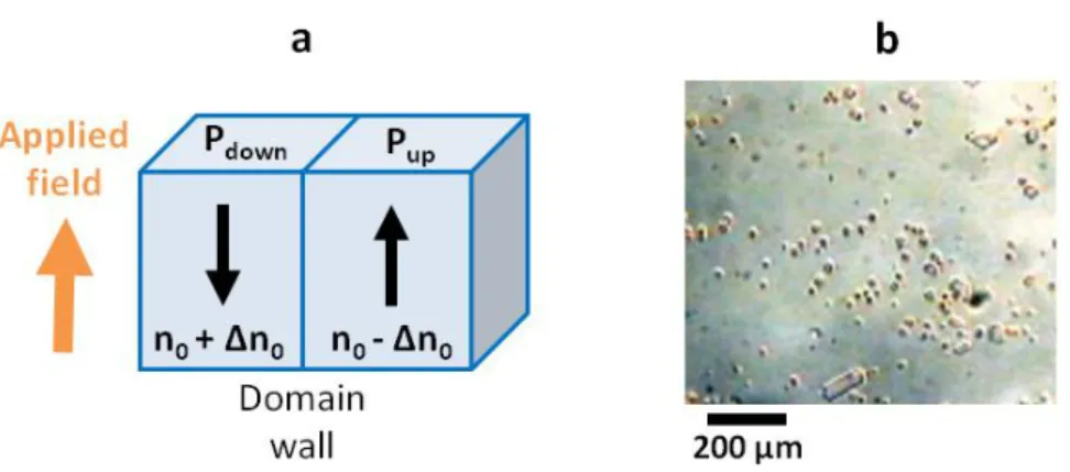
1.5. Screening of ferroelectric surfaces
As shown schematically in Fig. 1.4, in a ferroelectric material, the polar discontinuity at the bulk-terminated surface gives rise to a net fixed surface charge defined by , where is the spontaneous polarization and is the surface normal. These charges induce an electric field, called the depolarization field Ed, opposite to the spontaneous polarization. As in the case of a
two-plate capacitor, the depolarization field has an electrostatic energy proportional to the square of the surface charge. A monodomain state is therefore unfavorable due to the high depolarization field whereas if two domains of opposite polarizations are adjacent, the depolarization fields compensate each other and reduce the total electrostatic energy. In Fig. 1.4, we label “Pup” a domain that has a polarization pointing upward at the surface and
“Pdown” a domain that has a polarization in the opposite direction.
Figure 1.4| Schematic of a ferroelectric domain structure in thin film. Polarization (black arrows) gives
rise to a surface charge depicted by the plus and minus symbols. The depolarization field (Ed) induced by
the charges is drawn with a blue arrow.
The depolarization field can also be reduced by electric field arising from charges. Such screening is (i) external if the charges arise from adsorbates and (ii) internal if the screening charges arise from defects/doping.
In the case of free surfaces, external screening can be performed by the adsorption of molecules, such as water. Kalinin et al. have quantified the amount of screening charges ςs with
respect to the polarization charges ςpol[31]. In Fig. 1.5, three cases are distinguished: the surface is
(a) unscreened ςs = 0, (b) partially screened ςpol > - ςs, and (c) completely screened ςpol = - ςs. The
unscreened case is energetically unfavourable. The partially screened is very often observed in air[32,33] and may occur in ultra-high vacuum as well[34,35].
1. Ferroic materials and domain structures 9
Figure 1.5| Screening mechanisms. Schematics of polarization charges and screening charges for (a)
unscreened, (b) partially screened and (c) completely screened surfaces. In this schematic, polarization charges and screening charges are depicted by the plus and minus symbols, respectively.
Internal screening is the charge compensation arising from defects in the material: vacancies and dopants can lead to an excess of free charges in the sample that are available to screen the polarization charges[36]. In order to be efficient, internal screening requires the migration of the internal charges toward the surface. Therefore, it is more efficient when annealing the sample since temperature increases the mobility of free charges and also of ions in the material[37].
10 I. Domains and domain walls
2. Ferroelectric and ferroelastic domain walls
The interfaces between ferroic domains are called domain walls. Here, we present criteria to classify ferroelectric domain walls based on the profile of their order parameter or their inclination with respect to the ferroelectric axis. Then, we explain how ferroelectric and ferroelastic domain walls are observed by optical techniques. We also give estimations of their thickness. Finally, we present two intriguing and specific properties of domain walls: conductivity in ferroelectric domain walls and polarity in ferroelastic domain walls.
While these results are more general, most of the experiments described here have been performed on perovskites structures, which have a chemical formula ABO3 where A and B are
cations.
2.1. Classical approach: domain walls as interfaces
2.1.1. Types of ferroelectric domain walls
In ferroelectric materials, due to the piezoelectric coupling between the ferroelectric polarization and the strain, rotating the polarization away from the symmetry-allowed direction is energetically costly. Thus a 180°-ferroelectric domain wall between a Pdown and a Pup domain
can be considered as Ising-like, i.e. with no-in plane polarization associated with polarization rotation, as shown in Fig. 1.6(a)[38].
Figure 1.6| Different types of ferroelectric domain walls. (a) Ising type, (b) Néel type and (c) Bloch type.
Arrows represent the polarization. θN and θB are the maximum rotation angles of the polarization in the
2. Ferroelectric and ferroelastic domain walls 11
The typical profile of the polarization across a domain wall is derived from Landau theory as a hyperbolic tangent:
where P is the amplitude of the polarization, P0 the equilibrium value of the polarization far from
the domain wall, xn the spatial coordinate perpendicular to the domain wall and 2W the domain
wall thickness[40].
Magnetic domain walls present other types of profiles. Indeed, in magnetism, the spin is quantized and cannot change his magnitude across a domain wall. Instead, it rotates within the plane of the domain wall (Néel walls) or perpendicular to it (Bloch walls)[41], as shown in Fig. 1.6(b) and 1.6(c), respectively.
By analogy with magnetism, Bloch and Néel profiles have also been discussed for ferroelectrics. Recent Density Functional Theory (DFT) calculations have shown that the structure of 180°-ferroelectric domain walls can have a mixed Bloch-Néel-Ising character. For example, minimization of the energy of a 180° domain walls in lithium niobate by DFT leads to the maximum polarization components (Pn, Pt, Pz)max=(0.56, 1.99, 62.4) μC/cm2 where Pn and Pt
are the polarizations normal and transverse to the domain wall, respectively. Pn and Pt lead to
Néel (Fig. 1.6(b)) and Bloch-like (Fig. 1.6(c)) rotations by maximum rotation angles of θN = 0.55°
and θB = 1.52°[39], respectively.
2.1.2. Neutral and charged ferroelectric domain walls
A criterion to differentiate ferroelectric domain walls is their net charge. We illustrate this criterion on the case of 180°-domain walls.
An ideal 180°-domain wall is perfectly aligned with the direction of the ferroelectric axis and is therefore neutral (Fig. 1.7(a)). Fig. 1.7(b) shows the case where a head-to-head configuration of the polarization leads to a maximum positive charge at domain wall. A tail-to-tail configuration, as shown in Fig. 1.7(c) leads to a maximum negative charge at domain wall. Fig. 1.7(d) illustrates one case of a domain wall slightly inclined with respect to the ferroelectric axis, which has a partial positive charge.
12 I. Domains and domain walls
Figure 1.7| Charges at domain walls (side view). (a) Neutral, (b) charged head-to-head, (c) charged
tail-to-tail and (d) partially charged, inclined domain wall. Polarization is depicted by black arrows and domain walls are indicated by black lines.
Domain walls can be classified by the angle between the polarization directions of the neighboring domains. We discussed above the case of 180° domain walls, but other orientations are possible, such as 109° and 71° domain walls in bismuth ferrite[42].
2.1.3. Mechanical compatibility at ferroelastic domain walls
The orientation of the ferroelastic domain walls is usually determined by the requirement of mechanical compatibility between the two adjacent domains. Indeed, a randomly oriented domain wall can induce a large increase of the elastic strain in the material. This is energetically unfavorable.
Let the spontaneous strain in the adjacent domains A and B, be ε(A) and ε(B). Then, the orientation of the domain wall is such that the transformation of any geometrical figure, which lies in the plane of the domain wall, due to deformations ε(A) and ε(B), should be identical. This domain wall is said to be stress-free, since no additional elastic strain is involved[26].
Mathematically, the condition is satisfied if any vector in the domain wall fulfills the condition:
where εij(A) - εij(B) is a symmetric tensor with up to six independent components, xi and xj are
2. Ferroelectric and ferroelastic domain walls 13
tensors in all the possible orientation states of the domains, and obtained the complete set of equations of the permissible domain walls for all ferroelastic transitions[43].
Some of the equations of the permissible domain walls are derived from symmetry considerations only and have fixed orientations. This is the case for every mirror plane W which transform domain A into domain B. The precise orientation of the other domain walls, labeled W’, depends on the relative values of the coefficients of the spontaneous strain tensor[43].
2.1.4. Optical identification of domain walls
We will show in section 2.1.5 that ferroelectric and ferroelastic domain walls are of nanometer scale thickness. This makes challenging the localization of domain walls in a sample. At first sight, it requires experimental techniques with nanometric spatial resolutions such as atomic force microscopy[44,45] or transmission electron microscopy[18,46]. However, optical techniques, which have a spatial resolution restricted by the optical diffraction limit (about 0.5 μm at best), can still be used to localize domain walls.
Ferroelastic domains are visible with polarized light microscopy because the refractive index ellipsoid depends on the macroscopic spontaneous strain. Therefore, ferroelastic domain walls are easily localized and usually appear as small lines in an optical image[47]. However, non-ferroelastic ferroelectric 180°-domains are not visible with an optical microscope because the ellipsoid of the refractive indices is centrosymmetric. Therefore, other optical techniques, such as second harmonic generation (SHG) and Raman spectroscopy, are used.
SHG is observed in non-centrosymmetric materials and depends on the second-order electrical susceptibility. Due to the nonlinearity of the second-order electrical susceptibility, the incident light of frequency w generates a nonlinear polarization wave in the material that oscillates at twice the frequency (2w). This nonlinear polarization wave radiates light at 2w[48]. These photons form the SHG signal. At domain walls, the SHG signal is enhanced and is used to perform 3D profiles[49–51], as shown in Fig. 1.8. This could be the signature of local strain that could enhance the second-order electrical susceptibility at domain walls[51]. Since the spatial resolution of SGH is restricted by the optical diffraction limit, the signal observed at domain walls is always mixed with the signals of the surrounding domains.
14 I. Domains and domain walls
Figure 1.8| SHG on domain walls. Three dimensional visualization of inverted ferroelectric domains inside
LiNbO3 crystal by Čerenkov-type second harmonic generation laser scanning microscopy. Domain walls
appear in green. Domains have a too low intensity to appear on this image. Reproduced from [51].
Raman micro-spectroscopy is also used to visualize 180°-domain walls. The mechanisms at the origin of the contrast are complex and will be discussed in details in Chap. III. They involve a combination of effects resulting from the defect structure and the electric (strain) field in the vicinity of the domain walls. Here, we only mention that maps of the intensity of the Raman modes across ferroelectric domains clearly reveal domain walls (Fig. 1.9). They appear as thin black lines separating domains of identical intensity.
Figure 1.9| Raman micro-spectroscopy on domain walls. Map of the intensity of E(TO8) Raman mode.
Black lines are domain walls and grey contrast domains. Reproduced from [52]. No scale was given in the original figure but the domains are about 2 μm wide.
If an external electric field is applied to the crystal, the 180° domains can also be observed thanks to the electro-optic effect. The electro-optic effect produces a change of the refractive indexes nij in response to an electric field Ek:
with rijk the tensor of the electro-optic coefficients.
2. Ferroelectric and ferroelastic domain walls 15
In the case of an uniaxial ferroelectric, under an external electric field applied along the polarization axis, the refractive index n0 changes to n0 + Δn0 in one domain and to n0 - Δn0 in the
other, as sketched in Fig. 1.10(a). Under an optical microscope, this difference leads to a detectable light scattering, as shown in Fig. 1.10(b) where small hexagonal domains are visible[53,54]. At domain walls, the index changes by 2Δn0. Domain walls appear then as thin dark
or white lines at the border of the hexagonal domains. If the sample contains polar defects, such as in LiNbO3, the resulting internal electric field leads to a weak electro-effect and allows seeing
domain walls without applying an external electric field[55].
Figure 1.10| Electro-optic imaging. (a) Schematic showing the principle of electro-optic imaging at a 180°
domain wall. The refractive index increases when the applied electric field is antiparallel to the spontaneous polarisation and decreases when it is parallel. (b) Polarized light microscopy image taken in LiNbO3 under an external electric field of 21.6 kV/mm. Adapted from [53,54].
2.1.5. Domain wall thickness
The thickness of domain walls influences the physical properties of ferroelectric and ferroelastic materials. For example, it has been shown that the domain wall thickness affects the dielectric and piezoelectric responses of ferroelectric thin films[56]. It is also known that the width of 180° stripe domains in thin films is proportional to the square root of the crystal thickness[57,58] with a constant of proportionality expressed as a function of the domain walls thickness[59]. Thus,
a measurement of the domain wall thickness is important. Most of the studies so far have relied on X-ray diffraction (XRD) or transmission electron microscopy (TEM).
16 I. Domains and domain walls
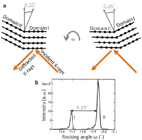
Figure 1.11| Diffraction on ferroelastic domains. (a) General principle of an X-Ray diffraction rocking
curve. In adjacent ferroelastic domains, atomic planes are not parallel. The crystal is rotated by an angle ω about an axis perpendicular to the plane of incidence in order to bring each atomic plane into Bragg’s condition. (b) A plot of integrated intensity as a function of angle ω, showing two peaks corresponding to domains in a single crystal of LaAlO3. Adapted from [60].
In a ferroelastic material, the diffracting planes are not aligned along the same directions in adjacent domains. For example, in Fig. 1.11(a), there is an angle of 0.25° between the crystal planes of two adjacent domains. If the sample is aligned such that the first domain is in Bragg condition, a rotation of ω = 0.25° about an axis perpendicular to the plane of incidence brings the second domain into Bragg condition. A plot of diffracted intensity as a function of ω shows two peaks corresponding to each domain (Fig. 1.11(b)).
In a ferroelastic sample with a high density of domains, a weak additional intensity is observed between the two domain-related peaks, as shown in Fig. 1.12. This intensity arises from the scattering of X-rays by atoms located in domain walls. The displacement of the atoms in domain walls is modeled by a hyperbolic tangent and the corresponding scattered intensity as a function of the incident angle is calculated for different thickness of the domain wall. A direct
2. Ferroelectric and ferroelastic domain walls 17
comparison between the results of the calculation and the experimental profiles gives an estimation the thickness of the domain walls[61–64].
Figure 1.12| X-Rays diffraction on domain walls: low intensity part of the rocking curve in lead phosphate
(Pb3(PO4)2). The weak additional intensity (indicated by the blue arrow) between the two peaks is due to
domain walls. Reproduced from [61].
TEM provides a direct measure of the thickness of domain walls. In this technique, an electron beam of electrons is transmitted through an ultra-thin sample, interacting with the sample as it passes through it. For a crystal, electrons are elastically scattered and an aperture in the back focal plane is used to image only electrons following the desired Bragg’s conditions. The domain wall appears as a region of width a few interatomic spacing with a slightly different contrast due to the small misorientation of the crystallographic planes in the domain wall[65]. If the domain wall thickness is less than the spatial resolution of the instrument, only a step is observed at the interface between domains. Recent experiments using high resolution TEM have revealed the domain wall profile to be in fair agreement with the accepted tangent hyperbolic profile[18,46].
The domain wall widths determined by XRD and TEM on several ferroelastic materials (CaTiO3, PbTiO3, Pb(Zr,Ti)O3, Pb3(PO4)2, YBa2Cu3O7-δ) lie in the range 0.2 to 5 nm[18,46,61–66].
The thickness of non-ferroelastic ferroelectric 180°-domain walls has also been determined with high-resolution TEM and found to be of the order of one unit-cell only[66].
18 I. Domains and domain walls
2.2. Renewed interest: domain wall engineering
The discovery of superconductivity localized at the ferroelastic domain walls of tungsten oxide has opened a new path of research[8]. For the first time, domain walls were seen as distinct elements with their own functional properties. The overall framework of applications arising from this research has been thought as “domain walls nanoelectronics”[21] or “domain boundary engineering”[22]. Within this vision, domain walls carry information and act as memory devices. In particular, Catalan et al. have proposed to reproduce the electronic logic circuits with domain walls[21]. A first success was obtained with a ferroelectric domain-wall diode, which allows a single direction of motion for all domain walls irrespective of their polarity, thanks to a thickness gradient in the sample[67].
2.2.1. Conductive domain walls in ferroelectrics
Higher conductivity at ferroelectric domain walls was reported in several ferroelectrics (Table 1.1). Investigations were performed with piezoelectric force microscopy (PFM) to identify the domain structure and with conductive-atomic force microscopy (c-AFM) to map the current.
Material DW Model Form Ref.
BiFeO3 109°
180°
Polarization discontinuity + reduction of the band gap
Thin film [9]
BiFeO3 71° Oxygen vacancies Thin film [11]
La-doped BiFeO3
109° Oxygen vacancies + reduction of the band gap
Thin film [12]
Pb(Zr,Ti)O3 180° Oxygen vacancies Thin film [10]
HoMnO3 - Polarization discontinuity + hole carriers Single crystal [16]
ErMnO3 - Polarization discontinuity + hole carriers Single crystal [15]
BaTiO3 90° Quasi-two-dimensional electron gas Single crystal [14]
LiNbO3 180° Inclined domain walls + UV illumination Single crystal [13] Table 1.1| Materials where conductive ferroelectric domain walls (DW) have been reported and the physical model used to explain the conduction. In HoMnO3 and ErMnO3, domain walls are curved and
have all possible orientations with respect to the polar axis.
Higher conductivity with respect to domains is observed at domain walls in BiFeO3 but
explain in the literature by two distinct mechanisms that may happen at the domain wall: a local reduction of the band gap[9,12] or the presence of charge defects near the domain wall[11,12].
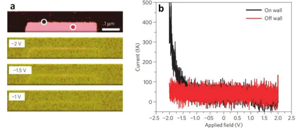
Current-voltage curves acquired at 109° and 180° domain walls reveal a Schottky-like behavior, as shown in Fig. 1.13, indicating that electrons have to overcome an energy barrier at the tip-sample interface[9]. In this case, this energy is reached for negative voltages below - 1.5 V.
2. Ferroelectric and ferroelastic domain walls 19
DFT calculations based on structural changes experimentally observed in TEM reveals a small change in the normal component of the polarization across the domain wall. Such a polarization discontinuity will be screened by free charges that will accumulate at the domain wall. This should enhance the conductivity. Other calculations also reveal a reduction of the electronic band gap in the domain wall that could lower the energy barrier at the tip-sample interface and facilitate the conduction[42].
Figure 1.13| Conduction at domain walls in BiFeO3. (a) (Top) Out-of-plane PFM image of a written 180°
domain in BiFeO3 and (lower) c-AFM current maps for -1, -1.5 and -2 V sample bias. Domain walls appear
as faint yellow lines. (b) I-V curves taken both on the domain wall (black) and inside the domain (red) reveal Schottky-like behavior in the domain wall. Reproduced from [9].
Current-voltage curves acquired at 71° domain walls also reveal a Schottky-like behavior[11]. If the voltage applied is below 3.5 V, the evolution of the current at the domain wall with temperature shows an Arrhenius behavior, current is increasing with temperature like in a semiconductor. The thermal activation energy deduced (0.7 eV) is too large for single electrons trap at oxygen vacancies but consistent with those at clusters of oxygen vacancies. Indeed, it was shown by first-principle calculations that oxygen vacancy clusters have an energy level located 0.6 eV below the conduction band while the energy level of single oxygen vacancies is located 0.11 eV below the conduction band (in SrTiO3)[68]. At higher voltages, both domain walls
and domains conduct. The low voltage regime is characterized by thermally activated electrons from oxygen vacancies states; the large voltage regime is regulated by the Schottky barrier between the tip and the sample. The barrier is lower at domain walls, probably due to an accumulation of oxygen vacancies.
20 I. Domains and domain walls
Conductivity arising from free electrons originating from oxygen vacancies is also reported at 109° domain walls in La-doped BiFeO3[12]. The main experimental result is that the current at
domain walls increases with increasing concentrations of oxygen vacancies.
Domain wall conductivity is observed along 180° domain walls in Pb(Zr,Ti)O3 and proposed
to be possible thanks to trap states, such as oxygen vacancies, within domain walls[10].
Higher conductivity with respect to domains is also reported in single crystals of HoMnO3[16]
and ErMnO3[15]. In these materials, the spontaneous polarization is not the primary
order-parameter and the domain walls are curved, taking all possible orientations with respect to the polar axis[69,70]. Figure 1.14(a) is a PFM image of the domains in ErMnO3: the arrows indicate the
orientation of the spontaneous polarization in the plane. Figure 1.14(b) shows the c-AFM image of the same area. Negatively-charged tail-to-tail domain walls show a higher conductivity than the domains, whereas at positively-charged head-to-head domain walls, the conductivity is suppressed. Since both materials are p-type semiconductors[71], the negative charges at tail-to-tail domain walls are screened by readily available mobile holes carriers. Furthermore, DFT calculations show that the polarization discontinuity at domain walls shifts the Fermi level into the valence band, where the hole mobility is high[15]. An increase of the conductivity at domain walls is then observed due to an increase of the density and mobility of hole carriers. At head-to-head domain walls, the hole density is lower than in the domains. Because free negative charges are scarce in p-type semiconductors, screening can only be achieved by cation vacancies that do not contribute to the conductivity[15]. The conductivity is then suppressed.
Figure 1.14| Conduction at domain walls in ErMnO3. (a) PFM image obtained In the yz-plane of an
ErMnO3 crystal. The inset shows a c-AFM image acquired at the same position. (b) c-AFM image of the
same area with polarization directions in-plane as-indicated. Domain walls appear as lines of different brightness. Reproduced from [15].
2. Ferroelectric and ferroelastic domain walls 21
A metallic-type giant domain wall conductivity (109 times higher than in the domains) is observed at 90° head-to-head domain walls in BaTiO3. It is interpreted within the framework of a
quasi-two-dimensional electron gas[14].
Higher conductivity is reported at 180° domain walls in single crystals of LiNbO3 but it
requires illumination with UV light[13]. This measurement was performed with small diodes that shined light on the sample during c-AFM imaging. The current is observed only under above-band gap illumination. It is higher when domain walls are slightly inclined with respect to the ferroelectric axis (angle < 0.25°). This inclination is controlled via doping with different concentrations of magnesium and all inclined domain walls are positively charged in this case. These positive carriers should increase the conductivity. UV-light seems to provide additional charges by creation of electron-hole pairs.
2.2.2. Polar domain walls in ferroelastics
By symmetry, all ferroelastic domain walls are polar, which will be briefly explained in the following. We consider a domain wall separating two ferroelastic domains constituting a so-called twin. The symmetry of the domain wall, which is the same as the symmetry of the twin, is the group of symmetry operations which leave the twin invariant. This is illustrated in Fig. 1.15, where the two ferroelastic domains are pictured by trapezoidal shapes reflecting the orientation of their spontaneous strain, and separated by a domain wall as a vertical plane. In this illustration, it is quite clear that the twin (and therefore the domain wall), is not invariant by inversion symmetry, even though both domains are centrosymmetric. This, in fact, is very general and it has been shown that all compatible ferroelastic domain walls are polar, and therefore can carry an electric polarization[72].
Figure 1.15| Symmetry of a ferroelastic domain wall. Schematic of a twin structure: domains are pictured
22 I. Domains and domain walls
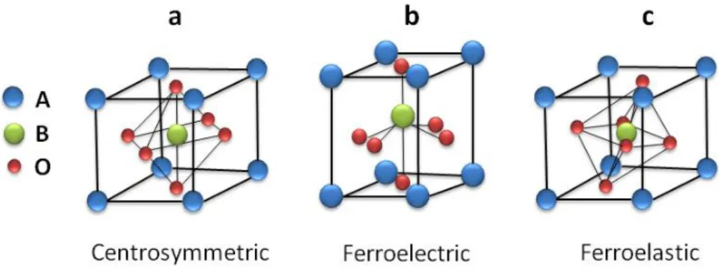
In order to give a microscopic description of the polarity in ferroelastic domain walls, we take the example of the perovskite structure. In the ideal cubic-cell represented in Fig. 1.16(a), atom A sits at cube corner positions (0, 0, 0), atom B at body-center positions (1/2, 1/2, 1/2) and oxygen atoms at face centre positions (1/2, 1/2, 0). The structure is centrosymmetric.
In a ferroelectric material, within the displacive model[73], the central atom B and the O atoms undergo a displacement along the polar axis, as shown in Fig. 1.16(b). This induces an off-centering of atom B with respect to the oxygen octahedron. The structure is not longer centrosymmetric and induces polarization.
Some ferroelastic materials present a cooperative rotation of the oxygen octahedra, as shown in Fig. 1.16(c).
Figure 1.16| Typical perovskite structures with chemical formula ABO3. (a) is centrosymmetric. (b) is
characterized by an off-centering of the B atom within the oxygen octahedron. (c) is characterized by a rotation of the oxygen octahedron.
In a perovskite, the rotation of the octahedra and the off-centering of the central atoms compete. Experiments tend to reveal an exclusion principle[47]: if an octahedron rotates, it does not show a ferroelectric displacement of its central atom. This is the case in SrTiO3 and CaTiO3.
When the rotation of the octahedron is prevented, a ferroelectric displacement becomes possible. This is the case in BaTiO3 and PbTiO3. The case of BiFeO3, where ferroelectricity coexists
with rotations of the octahedra is a noticeable exception[74].
We consider the example of adjacent ferroelastic domains characterized by rotations of the octahedra in opposite directions. At the intersection between the domains, i.e. at a domain wall, one way to obtain a stress-free interface is to suppress the octahedron rotation. Off-centering movements are then able to occur in domain walls, inducing polarization.
2. Ferroelectric and ferroelastic domain walls 23
This expectation is confirmed by computer simulations on CaTiO3[75]. Goncalves-Ferreira et
al. simulated a sample with two ferroelastic domain walls. Fig. 1.17(a) shows the oxygen octahedra rotation across the domain walls. It follows the hyperbolic tangent profile expected from Landau theory, with a domain wall thickness of 80 Å (consistent with the experimental value[18]). At the centre of the domain walls, indicated by vertical lines, the rotation is suppressed. Fig. 1.17(b) shows the off-centering of the central Ti atom with respect to the oxygen octahedra, as a function of the angle of rotation Q (for sake of simplicity, only the displacement along one direction is shown). Far from the domain wall, the rotation is large and the off-center displacement is null. At the domain wall, the angle of rotation is null and the Ti atom is slightly displaced: this implies a polar domain wall.
Figure 1.17| Competition between rotation of the octahedra and off-centering of Ti atoms. (a)
Octahedra rotation Q as a function of the position perpendicular to the domain wall. The dashed line is a fit to the expected hyperbolic tangent profile. The vertical lines indicate the position of domain walls. (b) Off-centering of Ti atoms along the x-coordinates within their corresponding O octahedron as a function of the octahedral rotation Q. Reproduced from [75].
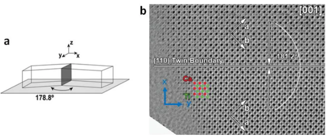
The first experimental evidence of polar domain walls in CaTiO3 was obtained by
aberration-corrected TEM[18]. Fig. 1.18(a) schematizes the domain wall geometry as imaged and Fig. 1.18(b) shows the TEM image obtained with a spatial resolution of 0.8 Å. Ca atoms appear as black features separated by Ti atoms. An angle of 181.2° (or equivalently 178.8°) is clearly identified between the two domains.
24 I. Domains and domain walls
Figure 1.18| TEM experiment on polar domain walls in CaTiO3. (a) Schematic of a single domain wall,
indicated as standing dark grey plane, with the chosen (x, y, z) reference system for the definitions of the measured displacements. (b) Amplitude of the reconstructed exit wave. The CaTiO3 crystal is imaged along
the [001] zone axis orientation, the (110) domain wall is indicated by the horizontal white line. Reproduced from [18].
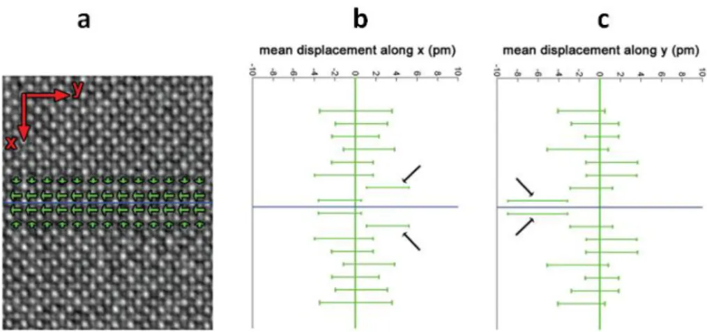
In order to determine the atomic positions, statistical parameter estimation theory was used. The interatomic distances between neighboring Ca-Ca and Ti-Ti columns were then calculated. It was found that the Ca-Ca distance is constant while the Ti-Ti distance changes near domain walls. Therefore, the analysis was focused on the off-centering of the Ti atomic position with respect to the neighboring four Ca atoms. Since these displacements were largely random and small, they were averaged in planes perpendicular to the domain wall. Next, the results in the planes above and below the domain wall were also averaged. The resulting displacements are shown in Fig. 1.19(a). Perpendicular to the domain wall, Ti atoms are shifted by 3.1 pm in the second closest layers pointing toward the twin wall (Fig. 1.19(b)). A larger displacement of 6.1 pm is measured parallel to the domain wall in the layer adjacent (Fig. 1.19(c)). It corresponds to a polarization of 0.04-0.2 C/m2, comparable with for example the value of bulk spontaneous polarization in the prototypical ferroelectric barium titanate, at room temperature.
2. Ferroelectric and ferroelastic domain walls 25
Figure 1.19| Atomic displacements at domain walls. (a) Phase of the reconstructed exit wave. Mean
displacements of the Ti atomic columns from the center of the four neighboring Ca atomic columns are indicated by green arrows. The blue horizontal line shows the position of the domain wall. (b,c) Displacements of Ti atomic columns in the x- and y-directions averaged along and in mirror operation with respect to the domain wall together with their 90% confidence intervals. Reproduced from [18].
A second experimental evidence of polar domain walls has been provided by SHG[19]. Indeed, SHG occurs only if the second-order electrical susceptibility is not null, which is possible only in a non-centrosymmetric (and therefore polar) structure. Two single crystals with different orientations were investigated. They presented a high density of domains, as illustrated in Fig. 1.20(a). Figure 1.20(b) shows a SHG image obtained by 1-μm scanning step in the plane parallel to the surface. Domain walls appear as bright lines while domains remain black, as expected for non-polar structures. The fact that domain walls are visible is, in itself, an evidence that they are polar. Several scans performed at different depths in the sample are used to obtain the 3D image of the domain wall through the sample.
Figure 1.20| SHG signal from domain walls. (a) Polarization microscope image taken in the crossed Nicol
configuration. A zoom-in picture of the enclosed square region is shown in the inset. (b) SHG section image. The observed area is the enclosed square in (a). Here X and Y axes with capital letters indicate the scanning axes of the SHG microscope. Reproduced from [19].
26 I. Domains and domain walls
The direction of the polarization in the domain walls was determined with polar diagrams. The principle is to record the SHG intensity at different positions along the domain wall for different polarization directions of the incident light; the polarization of the second harmonic signal is kept parallel to it. As an example, Fig. 1.21(a) shows the signal of an area containing three domain walls (labeled “TB1”, “TB2” and “TB3”) and Fig. 1.21(b) the corresponding polar diagrams mapping: each circle represents a 360° rotation of the polarization. The domain walls exhibit a double-wing diagram with a twofold symmetry. The variations of intensity are fitted in order to determine the direction of the polar axis with respect to the domain wall plane.
Figure 1.21| Orientation of the polarization in domain walls. (a) SHG image of an area that contains three
domain walls, labeled TB1, TB2 and TB3. The corresponding polar diagrams mapping is shown in (b). Reproduced from [19].
In the domain walls labeled “TB1” and “TB2”, the direction of the polar axis is inclined toward the normal of the domain wall plane. On the other hand, the polar axis is located in the domain wall plane, when adjacent domain walls are far, such as in “TB3”. This seems to indicate an interaction between domain walls, even separated by several micrometers. The result of the analysis is in contradiction with theoretical expectations where the polarity always lies in the domain wall plane[75].
Polar domain walls have also been reported in the non-polar material strontium titanate (SrTiO3)[76]. However, in SrTiO3 the domain wall polarity is thermally induced: on cooling, polarity
appears at 80 K while the ferroelastic transition point is at 150 K[76]. Furthermore, SrTiO3 is an
incipient ferroelectric, meaning that chemical[77] or isotopic substitution[78], as well as the application of stress[79] can easily induce ferroelectricity in the material. The mechanisms at the origin of the polarity in domain walls are therefore likely to be more complex than in CaTiO3.
3. Summary 27
3. Summary
We have shown in this chapter that ferroic materials spontaneously organize into domains, each with their own direction of the order parameter. The interfaces between adjacent ferroic domains are called domain walls. These domain walls, especially ferroelastic and ferroelectric, turn out to be interesting objects because of their unique physical properties that do not exist in the adjacent domains. In particular, conductivity at ferroelectric domain walls and polarity at ferroelastic domain walls have attracted a lot of attention[21,22]. The models proposed for the conduction at ferroelectric domain walls in BiFeO3, Pb(Zr,Ti)O3, ErMnO3, HoMnO3, BaTiO3 and
LiNbO3 are either based on (i) intrinsic properties[9,14–16], such as a local modification of the
band-gap or an accumulation of free charges due to a polarization discontinuity, or (ii) extrinsic properties[10–13], such as the interaction with defects. The same distinction is true for polar ferroelastic domain walls which are expected by symmetry in all ferroelastics but have been observed experimentally only in CaTiO3 and SrTiO3.
One of the main challenges in accessing a deeper understanding of domain walls is the availability of appropriate techniques to investigate the local characteristics of such domain walls.
The thesis stands at the crossroads between the development and use of appropriate techniques to study domain walls; and the research for fundamental understanding of domain walls properties.
In term of fundamental understanding, we are interested in the role of defects and free charges at ferroelectric domain walls. We also aim at a better understanding of the photo-conductivity observed at domain walls in LiNbO3. Finally it is our objective to investigate the
characteristics of the polarization in ferroelastic domain walls and to find ways to control this polarization, in view of devices applications.
Recognizing the difficulty in analyzing domain walls and aiming at extending the available breadth of techniques, we have laid emphasis on using techniques which have little or no previous applications on domain walls: we used Raman micro-spectroscopy to study the structural modifications near domain walls, dielectric spectroscopy to investigate the influence of defects, low energy electron microscopy and resonant piezoelectric spectroscopy to probe the electric response of domain walls.
29
II. Methods
The investigation of domain walls was performed with Raman micro-spectroscopy, low energy electron microscopy, dielectric spectroscopy and resonant piezoelectric spectroscopy. We review in this chapter the main characteristics of these techniques.
Dielectric spectroscopy and Raman micro-spectroscopy are complementary techniques used to probe the interaction between defects and ferroelectric non-ferroelastic domain walls. The former is a macroscopic, bulk measurement, while the latter gives a microscopic picture with a resolution limited by the optical diffraction limit.
Resonant piezoelectric spectroscopy and low energy electron microscopy are used to investigate the electric response in ferroelastic domain walls. The former probes the piezoelectric response of domain walls, while the latter can identify polarization surface charges near domain walls and study the influence of electron injection.
30 II. Methods
1. Raman spectroscopy
1.1. Harmonic theory of crystal vibrations
We consider a crystal with N atoms in its unit cell. The dynamic of the system is described by the small displacements of the atoms. The position of an atom at a given time is given by the sum of three vectors describing (1) the position of the unit-cell with respect to the one at the origin, (2) the position of the atom in the unit-cell and (3) the displacement of the atom with respect to its equilibrium position. The displacement of the jth atom in the mth unit-cell in the direction α with respect to its equilibrium position is written uα(mj).
To determine the equation of motions of the atoms, the potential energy φ of the crystal is expanded in Taylor series around the equilibrium point[80]:
with and
φ0 is the potential energy at equilibrium; it is constant and not of interest if we consider
vibrations: we set it to zero. φ1 is a linear combination of the small displacements and is null at
equilibrium. In the harmonic approximation, terms of order higher than two are neglected and the equations of motion can be written:
where Mj is the mass of the atom j and is the acceleration of the jth atom in the mth
1. Raman spectroscopy 31
atom in the mth unit-cell along the direction α when the (j’)th atom in the (m’)th unit-cell is displaced by a unit distance in the direction α’.
Because of the periodicity of the crystal, the coefficient does not depend
on the absolute position of the unit cell but only on its relative position with respect to the other unit-cells. Therefore, we are looking for solutions periodic in time and space, i.e. in the form of harmonic waves:
where is independent of the unit cell considered and is the equilibrium position of the jth atom in the mth unit-cell. The vector is the wave vector. It is normal to the wave front and its magnitude is equal to 2π/λ where λ is the wavelength of the wave.
Substitution of this ansatz in the equations of motion yields 3N eigenvalues and 3N eigenvectors, corresponding to atomic vibrations in (x, y, z). The eigenvalues appear as the squares of the frequencies of the vibrations and the eigenvectors give the relative displacement of the atoms associated with each vibrational mode[81].
These vibrations are called normal modes, to which are associated normal coordinates Q. For example, among these solutions, for , three have a frequency equal to zero and correspond to the translational movements of the full crystal.
1.2. LO-TO splitting
In ionic crystals, vibrations may carry a dipole moment. Such dipole moment change generates an electromagnetic field. Therefore, in order to determine the frequencies of these vibrations, it is necessary to solve the coupled equations of motion of the lattice and the electromagnetic field. One manifestation of this coupling is a frequency difference between the longitudinal and transverse optical modes near the Brillouin zone center, called LO-TO splitting[82].
Let us consider the case of a crystal of cubic symmetry. A vibration propagating in the y-direction can involve motion of atoms along the y, x or z -y-directions. We label the corresponding modes LOy(y), TOx(y) and TOz(y), respectively. All these modes vibrate at the same frequency
because of the crystal isotropy. However, if the motion of the atoms induces a dipole moment along the y-direction for LOy(y) and along the x or z-directions for TOx(y) and TOz(y), the
![Figure 1.1| Models of possible distortions of crystal structure. Reproduced from [26]](https://thumb-eu.123doks.com/thumbv2/123doknet/12852040.367958/15.892.172.679.582.1022/figure-models-possible-distortions-crystal-structure-reproduced.webp)
![Figure 1.2| Ferroic orders under the parity operations of space and time. Reproduced from [28]](https://thumb-eu.123doks.com/thumbv2/123doknet/12852040.367958/16.892.223.706.437.755/figure-ferroic-orders-parity-operations-space-time-reproduced.webp)