HAL Id: hal-01390933
https://hal.archives-ouvertes.fr/hal-01390933
Submitted on 2 Nov 2016HAL is a multi-disciplinary open access archive for the deposit and dissemination of sci-entific research documents, whether they are pub-lished or not. The documents may come from teaching and research institutions in France or abroad, or from public or private research centers.
L’archive ouverte pluridisciplinaire HAL, est destinée au dépôt et à la diffusion de documents scientifiques de niveau recherche, publiés ou non, émanant des établissements d’enseignement et de recherche français ou étrangers, des laboratoires publics ou privés.
Flexible Photodiodes Based on Nitride Core/Shell p-n
Junction Nanowires
H Zhang, Xing Dai, Nan Guan, Agnes Messanvi, Vladimir Neplokh, Valerio
Piazza, Martin Vallo, Catherine Bougerol, François H Julien, Andrey
Babichev, et al.
To cite this version:
H Zhang, Xing Dai, Nan Guan, Agnes Messanvi, Vladimir Neplokh, et al.. Flexible Photodiodes Based on Nitride Core/Shell p-n Junction Nanowires. ACS Applied Materials & Interfaces, Wash-ington, D.C. : American Chemical Society, 2016, 8, pp.26198 - 26206. �10.1021/acsami.6b06414�. �hal-01390933�
Flexible photodiodes based on nitride core/shell p-n
junction nanowires
Hezhi Zhang1 , Xing Dai1 , Nan Guan1 , Agnes Messanvi1,2,3 , Vladimir Neplokh1 , Valerio Piazza1 , Martin Vallo3 , Catherine Bougerol2,3 , François H. Julien1 , Andrey Babichev1,5 , Nicolas Cavassilas6 , Marc Bescond6 , Fabienne Michelini6 , Martin Foldyna7 , Eric Gautier2,8 , Christophe Durand2,3 , Joël Eymery3, and Maria Tchernycheva1,* 1
Centre de Nanosciences et de Nanotechnologies, UMR9001 CNRS, University Paris Sud,
University Paris Saclay, Orsay 91405, France
2
Université Grenoble Alpes, Grenoble 38000, France
3
“Nanophysique et Semiconducteurs” group, CEA, INAC-SP2M, 17 rue des Martyrs, Grenoble
38000, France
4
“Nanophysique et Semiconducteurs” group, CNRS, Institut Néel, 25 rue des Martyrs, Grenoble 38000, France
5
ITMO University, St. Petersburg 197101, Russia
6
Aix Marseille Université, CNRS, Université de Toulon, IM2NP UMR 7334, 13397, Marseille, France
7 LPICM-CNRS, Laboratoire de Physique des Interfaces et Couches Minces, Ecole
KEYWORDS: Flexible photodiode, nitride nanowires, InGaN, core/shell p-n junction,
self-powered photodetectors
ABSTRACT: A flexible nitride p-n photodiode is demonstrated. The device consists of a
composite nanowire/polymer membrane transferred onto a flexible substrate. The active element
for light sensing is a vertical array of core/shell p-n junction nanowires containing InGaN/GaN
quantum wells grown by MOVPE. Electron/hole generation and transport in core/shell
nanowires are modelled within non-equilibrium Green function formalism showing a good
agreement with experimental results. Fully flexible transparent contacts based on a silver
nanowire network are used for device fabrication, which allows bending the detector to a few
millimeter curvature radius without damage. The detector shows a photoresponse at wavelengths
shorter than 430 nm with a peak responsivity of 0.096 A/W at 370 nm under zero bias. The
operation speed for a 0.3×0.3 cm2
detector patch was tested between 4 Hz and 2 kHz. The -3 dB
cut-off was found to be ∼35 Hz, which is faster than the operation speed for typical photoconductive detectors and which is compatible with UV monitoring applications.
INTRODUCTION
The ultraviolet A (UVA) spectral region (320 – 400 nm) is a major component of the UV solar
radiation, which corresponds to more than 99 per cent of UV light that reaches the earth surface.
At high dose, UVA sunlight generates a severe oxidative stress in cells and is harmful for human
health, however moderate exposure to UVA can be favorable, in particular stimulating the
vitamin D generation1
. In this context, the development of wearable UV sensors helping people
to balance their sun exposure is today an important societal challenge2
. In addition to high
sensitivity and spectral selectivity, wearable UV sensors need to be lightweight and flexible in
order to be easily incorporated in skin patches or integrated on clothes. Autonomous operation
without external bias is also an important requirement for this application. Today, there exist a
large number of commercially-available UV sensors3
, however they remain rather bulky and
cannot be integrated directly on human clothes or skin4
. Today, nanomaterials are extensively
investigated for UV sensing as a way to enable high sensitivity combined with a possible
integration on fabric and self-powering5,6
.
Wide bandgap nanowire (NW) photodetectors can successfully respond to the
above-mentioned specifications for a wearable UV sensor. NW photoconductors based on nitride or
oxide materials were reported to exhibit a very high sensitivity thanks to the separation of
photogenerated carriers in radial direction7-11
. NW arrays are also reported to enhance the light
absorption by light trapping12
and antireflection13
effects, which can lead to a high sensitivity
even for a small amount of active material. The use of wide bandgap semiconductors naturally
provides spectral selectivity by the bandgap absorption cut-off without the use of additional
wavelengths of UVA shorter than 400 nm)14,15
. Finally, thanks to their small diameter, NWs can
stand large deformations without damage16,17
. This last property enables their use as an active
material for flexible optoelectronic devices18,19
.
Many realizations of flexible UV detectors have been reported, mainly based on ZnO
photoconductors20,21
. However, photoconductors, despite many efforts13
, still suffer from long
response time constants22
. The operation speed can be significantly enhanced by changing the
operation principle from a photoconductor to a photodiode15
. In addition, p-n photodiodes can
operate under zero bias without any need for external polarization, which is a major advantage
for their application as portable UV sensors.
The flexible detector fabrication typically follows one of the two approaches: direct NW
growth on plastic substrates13,20,23
or NW transfer to plastic by different methods such as
electro-spinning method24
, printing21,25
, dielectrophoretic positioning26
, etc. The direct growth on plastic
severely restricts the choice of the growth techniques (by limiting the growth temperature) and as
a consequence the NW materials that can be synthetized. Transfer methods are potentially
applicable to any NW material. However, for the majority of transfer methods, the NWs are
positioned horizontally on the substrate, which eliminates the benefit of absorption enhancement
in a NW ensemble due to light trapping. The initial NW orientation cannot be maintained.
Recently, an alternative transfer method yielding vertical NWs has gained a broad interest18, 19, 27, 28
. It is based on NW embedding in a polymer layer followed by either mechanical peeling of the
membrane18, 27
, or under-etching of a sacrificial layer19, 28
. Following this method, a flexible
Schottky photodiode based on CVD-grown GaN NWs has been demonstrated29
. Unfortunately,
deep defects in CVD-grown GaN wires yield a strong photoresponse in the visible spectral
defect-related absorption by the above-bandgap absorption, which can be better controlled in particular
by using ternary alloys for tuning the absorption edge. This is the objective of the present study.
In this work we demonstrate for the first time a flexible nitride p-n photodiode. The device
employs core/shell p-n junction NWs grown by metalorganic vapor phase epitaxy (MOVPE) on
sapphire substrates. InGaN/GaN quantum wells (QWs) are inserted in the active region to extend
the detection range to wavelengths longer than the GaN near band edge cut-off. We employ a
mechanical peeling transfer method18
, which allows to maintain the NW orientation. This is of
particular importance for the p-n NWs, for which the polarity of the junction should be preserved
for all wires contacted in parallel. The NWs were embedded into a polymer layer and the
polymer/NW membrane was mechanically peeled-off, contacted and mounted on a piece of a
copper tape. A fully flexible transparent contact based on a silver nanowire network was used,
which allows bending the detector to a few millimeters curvature radius without damage.
Without any external bias, the detector shows a photoresponse at wavelengths shorter than 430
nm with a peak responsivity of 0.096 A/W at 370 nm. The operation speed of a 0.3×0.3 cm2
detector patch was tested between 4 Hz and 2 kHz. The -3 dB cut-off was found to be ∼35 Hz, which is faster than the operation speed for typical photoconductive detectors and which is
compatible with UV monitoring applications. Angular dependence of the photoresponse was
analyzed.
EXPERIMENTAL SECTION
Nanowire Growth. The core-shell NWs containing GaN/InGaN multiple quantum wells
wires on sapphire is based on an in situ thin SiN layer deposition acting as a partial mask. The
vertical growth was favored by using a high flux of silane (200 nmol/min), a low V/III ratio (50),
a high temperature (1040 °C) and a high pressure (800 mbar) as described in detail in ref30
. A
first section of about 5 μm is grown with silane injection under trimethylgallium (TMGa)
precursor and ammonia (NH3) flux leading to a spontaneous SiNx passivation of the wire
sidewalls that maintains the wire geometry31, 32
and to a high n+
-type doping of the wire core
(donor concentration around ~1020
cm-3 33
). By stopping the silane flux, a second
non-intentionally doped section (1018
cm-3 34
) is grown to reach a length of about 25 μm. 30 radial
InGaN/GaN QWs are subsequently grown around the top unpassivated wire section
corresponding to the non-intentionally doped part at 400 mbar under the injection of
triethylgallium (TEGa), trimethylindium (TMIn) and ammonia at 720 °C for the InGaN wells
(In-content target about 18 %) and 900 °C for the GaN barriers. The nominal thickness is 3 nm
and 10 nm for the wells and barriers, respectively. A final p-GaN thick shell of about 150 nm is
grown at 920 °C with a biscyclopentadienyl-magnesium precursor (Cp2Mg) followed by a
dopant activation annealing performed at 750 °C for 20 min in N2 atmosphere (acceptor
concentration around ~1016
-1017
cm-334
).
The schematic of Figure 1 (a) illustrates the core/shell NW internal structure while Fig. 1 (b)
presents an SEM image of an as-grown NW array illustrating the wire morphology. The average wire height is 25±5 μm and the diameter is around 1-2 μm. The typical wire density is about 106
cm-2. We note that this growth procedure yields MQWs not only on the m-plane lateral sidewalls,
but also on the top -c plane, with a different QW thickness and In content35
.
The internal wire structure was probed by scanning transmission electron microscopy (STEM)
axis was prepared by focused ion beam (FIB) in order to observe the wire cross-section in
transversal direction. Figure 1 (c) shows STEM-HAADF images at three increasing
magnifications taken along the c-zone axis on the same wire transversal slice. A clear core-shell
structure is observed around wire sidewalls corresponding to m-planes facets evidencing the
presence of 30 InGaN/GaN MQWs followed by a p-type GaN shell. The thickness of InGaN wells in dark contract is estimated to be 7 ± 1 nm while the GaN barriers are 22 ± 2 nm. The thickness of the p-GaN surrounding shell is measured to be ∼175 nm. We observe that the external interface of the wells (corresponding to the InGaN/GaN interface) is significantly
rougher compared to the internal well interface (corresponding to the GaN/InGaN interface), as
generally observed for InGaN/GaN heterostructures, especially with thick wells. The In-content
in the well has been estimated close to 15%36
instead of the targeted 18% due to lower
incorporation of In on the m-plane surfaces37
. In Figure 1(c), we observe that the MQW structure
can be disturbed by dislocations and stacking faults originating from the first QW interface that
propagates across the whole shell heterostructure. These morphological properties of the
core-shell structure are consistent with the previously reported core-core-shell structures grown under
similar growth conditions for photovoltaic applications38
Figure 1. a) Schematic of the core-shell MQW NW structure. b) SEM image of the NW array. c)
Transversal cross-sectional STEM-HAADF images taken along the c-zone axis evidencing the
core-shell structure on m-plane hexagonal facets (wire slice prepared by FIB technique). The
increasing magnification of TEM images reveals that the shell is composed of 30×InGaN
(7nm)/GaN (22nm) MQWs coated with a thick p-GaN layer. d) µPL of a single NW measured at
4K.
The optical properties of NWs were investigated by low temperature micro-photoluminescence
(µPL) spectroscopy. In order to avoid excitation of multiple NWs, the NWs were cut from their
substrate by an ultrasonic bath and dispersed with a low density on a Si substrate. The μPL
characterization was carried out at 4 K by exciting single NWs at 375 nm wavelength by a
and a charge coupled device (CCD) camera. Figure 1 b) shows a typical µPL spectrum of a
single NW. The spectrum presents two contributions. The main peak at 3.07 eV (403 nm) is
attributed to the radial QWs on the m-plane. A weak shoulder peak observed at a lower energy
around 2.8 eV (442 nm) originates from the axial QWs at the top part of the NW as previously
reported in ref35
.
Flexible Photodetector Fabrication. The fabrication of flexible photodetectors started by
forming an ohmic contact to the p-GaN shell. A photoresist layer was spin-coated on the
as-grown NWs to protect the highly n-doped GaN base of the NWs. Then a semi-transparent 3 nm/3
nm Ni/Au metallic layer was deposited by e-beam evaporation on the p-GaN shells protruding
from the resist. The metal was lifted-off and the sample was annealed at 400 °C in air for 10 min.
The presence of this thin Ni/Au layer allows to form an ohmic contact to the p-GaN shells. The
NWs were then encapsulated into polydimethylsiloxane polymer (PDMS) with an average
thickness of 25 μm. The composite nanowire/PDMS membrane was peeled-off from the sapphire
substrate and flipped upside down to metalize the bottom part of the NWs. An ohmic
Ti/Al/Ti/Au (10 nm/30 nm/10 nm/200 nm) contact was deposited on the NW highly n-doped
bases. Then the device was again flipped upside-down and transferred to a flexible substrate
(copper tape). The transparent top contact was deposited by spin-coating on the surface using a
suspension of silver nanowires to achieve a flexible network connecting the p-GaN shells. The
contact area is approx. 0.3×0.3 cm2
. The fabrication process is schematically illustrated in figure
2 (a). The SEM image (figure 2(b)) shows a bird's eye view of the device. The distribution of
silver nanowires is uniform. The GaN NWs are well connected by silver nanowires as illustrated
silver nanowires is ∼1.2×10⁶
cm-2
. Fig. 2d) presents a photo of the device and illustrates its
flexibility.
Figure 2. a) Schematic representation of the fabrication steps : encapsulation in PDMS and
peel-off of the membrane; deposition of the back metal contact; deposition of the top transparent
contact composed of a silver nanowire mesh. b) Bird's eye view SEM image of the top surface of
the detector. c) Top view SEM image of an individual nitride NW contacted with silver
nanowires. d) Device photo illustrating its flexibility.
We note that the main challenge in the fabrication process is the realization of a flexible
transparent ohmic contact. For the bottom opaque contact, a standard metallization is used,
which provides an ohmic contact to the n-GaN NW bases. Metal contacts were shown to well
sustain bending deformations for curvature radiuses of several millimeters39-43
. Therefore, they
are commonly used for flexible LEDs and photodetectors44, 45
. However, standard metal contacts
are opaque and do not allow for light coupling into the NW photodiode. Following our previous
developments, we have chosen a silver nanowire mesh as a top transparent contact18
contacts is today intensively studied in the literature as an alternative to ITO, which combines
mechanical flexibility with optical transparency and low resistance46, 47
.
Flexible photodetector characterization techniques. The electrical characteristics of the
flexible photodetector were investigated using a Janis probe station and a Keithley 2636
source-meter at room temperature. The spectral dependence of the photocurrent was analyzed by
illuminating the device with a wavelength tunable Xenon lamp light coupled with a Jobin Yvon
Triax 180 spectrometer. A calibrated photodiode sensor was used to measure the light source
output intensity, which was then used to normalize the photocurrent spectra. The photo
responsivity of the detector was calibrated using a continuous wave laser diode emitting at 375
nm wavelength. In addition, electron beam induced current (EBIC) measurements were
performed to probe the top contact properties. EBIC maps were collected at room temperature
using an acceleration voltage of 20 kV in a Hitachi SU8000 SEM controlled by Gatan Digiscan
system as described in ref48
.
RESULTS AND DISCUSSION
Electrical characterizations. A current-voltage (I-V) curve in the dark of the fabricated
flexible photodetector is displayed in Figure 3 a). The curve exhibits a typical rectifying behavior
with a diode knee voltage around 2.3 V, after which the forward current increases steeply. Under
reversed bias, the leakage current is negligible up to -3 V. The diode-like I-V characteristic
validates the fabrication procedure, showing that the PDMS membrane provides a good electrical
measurements were repeated after 50 cycles of device bending down to a radius of 5 mm. No
modification of the I-V curve was observed.
To probe the electrical connection between the silver nanowires and the nitride NWs and to
evaluate the long range conductivity of the silver nanowire top contact, EBIC mapping was
performed on the flexible photodetector. Figure 3 b) and c) presents the SEM image and the
EBIC map (under zero bias) of the top surface of the detector. The electron beam arriving at the
sample surface creates electron-hole pairs in the core/shell nitride NWs, which are separated by
the internal electrical field of the p-n junction and then collected by the electrodes48
. The induced
current appears as a bright contrast in figure 3 c). The region probed by EBIC in Figure 3 is
located 1 mm away from the metal bonding pad and there is no current spreading grid on top of
the silver nanowire network. No significant attenuation of the EBIC signal with distance from
the bonding pad is observed, which proves that the carrier transport by the silver nanowires
network is efficient. By comparing the SEM and the EBIC maps, we evaluated the number of
nitride NWs protruding from PDMS (and thus contacted by silver nanowire) and the number of
NWs generating EBIC signal. As an example, the positions of the NWs are highlighted with
green hexagons in the upper right part of the maps. The number of NWs generating EBIC signal
corresponds to 85% of all protruding NWs. This value gives an estimation of the yield offered by
Figure 3. a) I-V curve of the flexible photodetector. b) Top-view SEM image of the detector
contacted with silver nanowires and c) the corresponding EBIC map (bright contrast corresponds
to the induced current in nitride NWs).
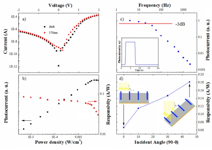
Electro-optical characterizations. The inset of Figure 4 (a) shows the I-V curves of the
detector in the dark and under illumination with UV light (λ = 370 nm, 1.26 × 10⁻⁸
W power) in
logarithmic scale. Under zero bias, the photocurrent is negative, the corresponding responsivity is ∼0.1 A/W. Under forward bias, the photocurrent changes sign at ∼0.25 V. This relatively low value may be related to some defects in the active region.
The power dependence of the responsivity has been probed by illuminating the detector with
an Ar++ ion laser (λ=244 nm) and varying the incident power density by almost 4 orders of
magnitude (from 5 ×10⁻⁶
W/cm2
to 7 × 10⁻³
W/cm2
). As shown in Fig. 4 b), at moderate excitation
power densities (up to ~ 3 ×10⁻³
W/cm2
), the photocurrent presents almost a linear dependence
with power. The responsivity slightly decreases from 0.084 A/W to 0.057 A/W in this region. At
high power densities the photocurrent dependence becomes sub-linear and the photocurrent
saturates. Correspondingly, the responsivity decreases down to 0.03 A/W at 7 ×10⁻³
W/cm2
photodiodes the response is linear up to higher power densities (0.2 W/cm250
). The saturation at
high excitation is related to the screening of the built-in field by the photogenerated carriers.
The detector operation speed was analyzed. First, the detector response to a square light pulse (λ=370 nm) was measured under zero bias. The inset of Figure 4 c) shows the temporal current trace. The flexible photodetector presents a fast response with a rise and decay switching time
below 0.1 sec (which is the time resolution of our measurement system). To further investigate
the device operation speed, the frequency dependence of the photocurrent was measured at zero
bias using a mechanically chopped illumination and a lock-in detection. Figure 4 c) shows the
detector frequency response from 4 Hz to 2000 Hz. The -3 dB cut-off frequency of the large area
(0.3×0.3 cm2
) device is ~ 35 Hz. This operation speed is higher than the typical values for NW
photoconductors 8, 11
and is comparable to the one of the axial p-i-n NW photodiodes49
. We note
that it is compatible with the potential application of UV monitoring.
The angular dependence of the photodetector responsivity was investigated. The photocurrent
was collected under zero bias for incident angles θ between 0 and 45 degrees for a power density
of 0.001 W/cm2
(i.e. in the range where the photocurrent shows an almost linear dependence on
the incident power as shown in Fig.4 b). As reported in Figure 4 d), the responsivity increases
with the incident angle. The responsivity is ∼0.066 A/W for the laser light perpendicular to the sample surface, whereas it increases to 0.18 A/W for a 45 degree tilt. This phenomenon can be
explained by the enhanced light harvesting when the sample is rotated. Indeed, the density of
nitride NWs obtained by self-catalyzed MOVPE growth is low, they cover only 3.82% of the
total detector surface. At normal incidence, only a small part of the NW surface (mainly their top
surface) absorbs light, as illustrated in the inset of Figure 4 d). The effects of light concentration
reported for nanowire solar cells51
µm range that are used in this study. When the photodetector is tilted, the light is absorbed not
only by the top surface but also by the NW side walls, which increases the portion of the
absorbed light and induces a stronger photocurrent for the same power density.
Figure 4. a) I-V curve in the dark and under illumination with λ = 370 nm. b) Power dependence
of the responsivity. c) Frequency response of the detector. Inset shows the current trace under
zero bias in response to a square light pulse. d) Angular dependence of the responsivity at
different angles from θ = 0 degree to 45 degree. Insets show schematics explaining the
The spectral response of the detector was analyzed. Figure 5 displays the room temperature
photocurrent spectra in logarithmic scale under zero bias and under reverse bias of -0.5 V,
respectively. The low-energy onset of the photocurrent (i.e. the energy value, for which the
photocurrent clearly dominates over the noise) is around 2.88 eV (430 nm). At higher energies,
the photocurrent increases by more than one order of magnitude, reaching its maximum at 3.35
eV (370 nm) and then slightly decreasing. The bandgap of the radial QWs is estimated to be
close to 3.03 eV (410 nm) at room temperature (according to µPL measurements discussed
above and accounting for the Varshni shift with temperature). Therefore, the low-energy onset
value of the photocurrent is below the bandgap of the radial QWs. This is most likely due to the
contribution to the photocurrent of the axial QWs, which have a smaller bandgap value due to
both their higher In concentration and to the quantum confined Stark effect induced by the
internal electric field along the c-axis. Nevertheless, the overall spectral response matches quite
well the UVA spectral domain, which validates the possible application of the developed
photodiode for UVA sensing.
The peak responsivity of the detector reaches its maximum value of 0.096 A/W at 3.35 eV. We
note that the density of the active NWs is quite low in the present device, a higher value can be
reached with a higher density NW array. A decrease of the photocurrent for energies above
3.4 eV is observed (the responsivity drops to 0.063 A/W at 4.1 eV). This decrease is typical also
for thin film nitride photodiodes and can be attributed to the high absorption coefficient of GaN
above the bandgap, which makes the absorption depth small. The carriers are generated close to
the surface of the p-doped GaN layer and have a large probability to recombine on surface states
before being collected. Same explanation can be applied in the present case for the enhanced
remains similar whereas the photocurrent signal increases. The peak responsivity becomes 0.157
A/W. In agreement with theoretical modeling presented in the next section, this signal
enhancement is attributed to the increase of the electric field in the active region facilitating the
carrier extraction from the QWs. For energies above the GaN bandgap the signal increase under
reverse bias can also be due to a slight broadening of the space-charge region in the p-n junction.
Figure 5. Room temperature photocurrent spectrum in logarithmic scale under zero bias and
under reverse -0.5 V, respectively.
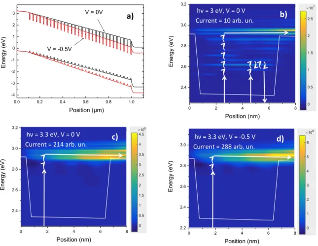
Modeling of current generation in the active region. The photocurrent generation in the
InGaN/GaN p-n junction QWs has been modeled using the non-equilibrium Green function
formalism. This model is described in details in ref52
. This approach considers the quantum
character of electrons, which cannot be neglected in the present device with an active region
containing QWs, since in QWs the confinement and the tunneling both control the electronic
transport. Moreover, as we show, the electron-phonon scattering has also a key role in the
photodetector operation.
InGaN/GaN MQWs with a nominal composition of 18%. The calculations are performed for
zero external bias and for -0.5 V reverse bias. Zero of energy corresponds to the Fermi level in
the p-GaN layer. The built-in field of the p-n junction is distributed homogeneously over the 29
left QWs which are empty in the dark. Only the first QW next to the n-GaN layer is filled with
electrons. The electron density in this well is 1018
and 1.3×10¹⁸
cm-3
at -0.5 and 0 V, respectively.
Due to the computational burden of the method, the photocurrent is only calculated for one
representative QW. The procedure is described in ref53
. To illustrate the evolution of the
photocurrent with the photon energy, Figures 6 b) and c) present the current maps as a function
of position and energy in the conduction band of a QW in an unbiased p-n junction under
illumination with 3 eV (i.e. deep in the InGaN QW) and with 3.3 eV (i.e. slightly below the
barrier bandgap), respectively. The calculation predicts that the responsivity increases by a factor
of 21 when the photon energy increases. This prediction is in qualitative agreement with the
experimental results shown above, for which the photocurrent signal increases ~9 times between
3 eV and 3.3 eV (cf. Figure 5). As shown by the quantification of the spectrum presented in Fig.
6 a), when electrons are generated deep in the well, the scattering with phonons controls the
extraction (the optical phonon energy is 92 meV). The interaction with phonons is schematically
illustrated with curved arrows in Fig 6 b), c) and d). In this case, a large number of
phonon-absorption is necessary to extract the photogenerated carriers from the QW. This current is then
expected to increase with temperature. In contrast, as shown in Fig. 6 c) for excitation with a
photon energy of 3.3 eV, the electrons can be withdrawn from the well without a large number of
phonon scatterings. The electronic extraction is then easier and the current is larger.
To simulate the photodetector response under bias, the photocurrent for a reverse bias of -0.5
region with the reverse bias. The corresponding current spectrum for the incident photon energy
of 3.3 eV is shown in Fig. 6 d). The model predicts the current increase by a factor of 1.34 under
bias, which is in qualitative agreement with the experimental value of 1.61 (cf. Figure 5)). By
comparing the spectra presented in Fig. 6 c) and d), it is clear that the reverse bias facilitates the
direct extraction of photogenerated carrier without any scattering with phonons. However, the
tunneling is not observed since the barriers are too thick.
Figure 6. a) Conduction band and valence band potential profiles in the entire active region for
external biases of 0 V and -0.5 V. Photocurrent spectra in conduction band versus position in a
extraction of carriers. The vertical arrows represent the interband interactions (photon
absorption/emission). The curved arrows represent the intraband interactions (phonon
absorption/emission). The horizontal arrows represent the diffusion process.
CONCLUSIONS
In conclusion, a flexible nitride p-n photodiode has been demonstrated using core/shell p-n
junction NWs containing InGaN/GaN QWs. The polymer membranes embedding active nitride
NWs were contacted using a transparent silver nanowire mesh to ensure high mechanical
flexibility. Without any external bias, the detector shows a photoresponse at wavelengths shorter
than 430 nm with a peak responsivity of 0.096 A/W at 370 nm. The -3 dB cut-off frequency for a
0.3×0.3 cm2
detector patch was found to be ∼35 Hz, which is compatible with UV monitoring applications. The detector photoresponse increases for an oblique incidence angle due to an
increased light absorption.
AUTHOR INFORMATION Corresponding Author
*Tel.: +33 1 69 15 40 51. E-mail: [email protected] (M.T.).
Notes
The authors declare no competing financial interest.
ACKNOWLEDGMENTS
This work has been partially financially supported by ANR “Investissement d'Avenir”
ANR-14-CE26-0020-01 project ‘PLATOFIL’, and by EU ERC project “NanoHarvest” (grant no.
639052). A. Babichev acknowledges the support of RFBR (project № 15-02-08282, №
16-29-03289), and program of fundamental research of the Presidium of the RAS №1 (project №
1.3.3.3). The device processing has been performed at CTU-IEF-Minerve technological
REFERENCES
(1) Holick, M. F. Sunlight and Vitamin D for Bone Health and Prevention of Autoimmune
Diseases, Cancers, and Cardiovascular Disease. Am. J. Clin. Nutr. 2004, 80 (6), 1678S–1688S.
(2) Zhang, X.; Xu, W.; Huang, M. C.; Amini, N.; Ren, F. See UV on Your Skin: an Ultraviolet
Sensing and Visualization System. In Proceedings of the 8th International Conference on Body
Area Networks, Boston, US, Sept 30th – Oct 2, 2013; Suzuki, J., Wang, H. Eds.; ICST, 2013;
Pages 22-28. DOI: http://dx.doi.org/10.4108/icst.bodynets.2013.253701
(3) http://www.solarmeter.com. accessed on July 31, 2016
(4) Tang, S. L. P. Recent Developments in Flexible Wearable Electronics for Monitoring Applications. Trans. Inst. Meas. Control 2007, 29 (3-4), 283–300 .
(5) Chen, H.; Liu, K.; Hu, L.; Al-Ghamdi, A. A.; Fang, X. New Concept Ultraviolet
Photodetectors. Mater. Today 2015, 18 (9), 493–502.
(6) Pang, C.; Lee, C.; Suh, K. Y. Recent Advances in Flexible Sensors for Wearable and Implantable Devices. J. Appl. Polym. Sci. 2013, 130 (3), 1429–1441.
(7) Calarco, R.; Marso, M.; Richter, T.; Aykanat, A. I.; Meijers, R.; vd Hart A.; Stoica, T.;
Lüth, H. Size-Dependent Photoconductivity in MBE-Grown GaN-Nanowires. Nano Lett. 2005, 5
(5), 981–984.
(8) Soci, C.; Zhang, A.; Xiang, B.; Dayeh, S. A.; Aplin, D. P. R.; Park, J.; Bao, X. Y.; Lo, Y.
H.; Wang, D. ZnO Nanowire UV Photodetectors with High Internal Gain. Nano Lett. 2007, 7 (4),
(9) Zhang, H.; Babichev, A. V.; Jacopin, G.; Lavenus, P.; Julien, F. H.; Egorov, A. Y.; Zhang,
J.; Pauporté, T.; Tchernycheva, M. Characterization and Modeling of a ZnO Nanowire
Ultraviolet Photodetector with Graphene Transparent Contact. J. Appl. Phys. 2013, 114 (23),
234505.
(10) Babichev, A. V.; Zhang, H.; Lavenus, P.; Julien, F. H.; Egorov, A. Y.; Lin, Y. T.; Tu, L.
W.; Tchernycheva, M. GaN Nanowire Ultraviolet Photodetector with a Graphene Transparent
Contact. Appl. Phys. Lett. 2013, 103 (20), 201103.
(11) González-Posada, F.; Songmuang, R.; Den Hertog, M.; Monroy, E. Room-Temperature
Photodetection Dynamics of Single GaN Nanowires. Nano Lett. 2011, 12 (1), 172–176.
(12) Garnett, E.; Yang, P. Light Trapping in Silicon Nanowire Solar Cells. Nano Lett. 2010, 10
(3), 1082–1087.
(13) Zhang, H.; Hu, Y.; Wang, Z.; Fang, Z.; Peng, L. Performance Boosting of Flexible ZnO
UV Sensors with Rational Designed Absorbing Antireflection Layer and Humectant
Encapsulation. ACS Appl. Mater. Interfaces 2016, 8 (1), 381–389.
(14) Bugallo, A.; Rigutti, L.; Jacopin, G.; Julien, F. H.; Durand, C.; Chen, X. J.; Salomon, D.;
Eymery, J.; Tchernycheva, M. Single-Wire Photodetectors Based on InGaN/GaN Radial
Quantum Wells in GaN Wires Grown by Catalyst-Free Metal-Organic Vapor Phase Epitaxy.
Appl. Phys. Lett. 2011, 98 (23), 3107.
(15) Zhang, H.; Messanvi, A.; Durand, C.; Eymery, J.; Lavenus, P.; Babichev, A.; Julien, F.
(16) Espinosa, H. D.; Bernal, R. A.; Minary‐Jolandan, M. A. Review of Mechanical and
Electromechanical Properties of Piezoelectric Nanowires. Adv. Mater. 2012, 24 (34), 4656–4675.
(17) Stan, G.; Krylyuk, S.; Davydov, A. V.; Cook, R. F. Bending Manipulation and
Measurements of Fracture Strength of Silicon and Oxidized Silicon Nanowires by Atomic Force
Microscopy. J. Mater. Res. 2012, 27 (03), 562–570.
(18) Dai, X.; Messanvi, A.; Zhang, H.; Durand, C.; Eymery, J.; Bougerol, C.; Julien, F. H.;
Tchernycheva, M. Flexible Light-Emitting Diodes based on Vertical Nitride Nanowires. Nano
Lett. 2015, 15 (10), 6958–6964.
(19) Chung, K.; Beak, H.; Tchoe, Y.; Oh, H.; Yoo, H.; Kim, M.; Yi, G. C. Growth and
Characterizations of GaN Micro-Rods on Graphene Films for Flexible Light Emitting Diodes.
APL Mater. 2014, 2 (9), 092512.
(20) Farhat, O. F.; Halim, M. M.; Abdullah, M. J.; Ali, M. K. M.; Ahmed, N. M.; Allam, N. K.
Growth of Vertically Aligned ZnO Nanorods on Teflon as a Novel Substrate for Low-Power
Flexible Light Sensors. Appl. Phys. A 2015, 119 (4), 1197–1201.
(21) Liu, X.; Gu, L.; Zhang, Q.; Wu, J.; Long, Y.; Fan, Z. All-printable Band-Edge Modulated
ZnO Nanowire Photodetectors with Ultra-High Detectivity. Nat. Commun. 2014, 5, 4007.
(22) Dai, X.; Tchernycheva, M.; Soci, C.; Compound Semiconductor Nanowire
Photodetectors. In Semiconductors and Semimetals, Dayeh, S. A., i Morral, A. F., Jagadish, C,
Eds.; Semiconductor Nanowires II: Properties and Applications; Academic Press: Burlington,
(23) Chen, T. P.; Young, S. J.; Chang, S. J.; Hsiao, C. H.; Wu, S. L. Photoelectrical and
Low-Frequency Noise Characteristics of ZnO Nanorod Photodetectors Prepared on Flexible Substrate.
IEEE Trans. Electron Devices 2013, 60 (1), 229–234.
(24) Zheng, Z.; Gan, L.; Li, H.; Ma, Y.; Bando, Y.; Golberg, D.; Zhai, T. A Fully Transparent
and Flexible Ultraviolet–Visible Photodetector Based on Controlled Electrospun ZnO‐CdO
Heterojunction Nanofiber Arrays. Adv. Funct. Mater. 2015, 25 (37), 5885–5894.
(25) Chen, G.; Liang, B.; Liu, Z.; Yu, G.; Xie, X.; Luo, T.; Xie, Z.; Chen, D.; Zhu, M.-Q.;
Shen, G. High Performance Rigid and Flexible Visible-Light Photodetectors based on Aligned X
(In, Ga) P Nanowire Arrays. J. Mater. Chem. C 2014, 2 (7), 1270–1277.
(26) Guilera, J.; Fàbrega, C.; Casals, O.; Hernández-Ramírez, F.; Wang, S.; Mathur, S.;
Udread, F.; De Luca, A.; Alie, S. Z.; Romano-Rodríguez, A.; Prades, J. D.; Morantea, J. R.
Facile Integration of Ordered Nanowires in Functional Devices. Sens. Actuators, B 2015, 221,
104–112.
(27) Spurgeon, J. M.; Boettcher, S. W.; Kelzenberg, M. D.; Brunschwig, B. S.; Atwater, H. A.; Lewis, N. S. Flexible, Polymer-‐Supported, Si Wire Array Photoelectrodes. Adv. Mater. 2010, 22 (30), 3277–3281.
(28) Lee, C. H.; Kim, Y. J.; Hong, Y. J.; Jeon, S. R.; Bae, S.; Hong, B. H.; Yi, G. C. Flexible
Inorganic Nanostructure Light-Emitting Diodes Fabricated on Graphene Films. Adv. Mater.
(29) Shi, X.; Peng, M.; Kou, J.; Liu, C.; Wang, R.; Liu, Y.; Zhai, J. A Flexible GaN Nanowire
Array-Based Schottky Type Visible Light Sensor with Strain‐Enhanced Photoresponsivity.
Adv. Electron. Mater. 2015, 1 (12), 1500169–1500175.
(30) Koester, R.; Hwang, J. S.; Durand, C.; Dang, D. L. S.; Eymery, J. Self-Assembled Growth
of Catalyst-Free GaN Wires by Metal – Organic Vapour Phase Epitaxy. Nanotechnology 2010,
21, 015602.
(31) Eymery, J.; Salomon, D.; Chen, X. J.; Durand, C. Process for Catalyst-Free Selective
Growth on a Semiconductor Structure. Patent WO/2012/136665, April 03 2012.
(32) Tessarek, C.; Heilmann, M.; Butzen, E.; Haab, A.; Hardtdegen, H.; Dieker, C.; Spiecker,
E.; Christiansen, S. The Role of Si during the Growth of GaN Micro- and Nanorods. Cryst.
Growth 2014, 14, 1486–1492.
(33) Tchoulfian, P.; Donatini, F.; Levy, F.; Amstatt, B.; Dussaigne, a.; Ferret, P.; Bustarret, E.;
Pernot, J. Thermoelectric and Micro-Raman Measurements of Carrier Density and Mobility in
Heavily Si-Doped GaN Wires. Appl. Phys. Lett. 2013, 103, 202101.
(34) Tchoulfian, P.; Donatini, F.; Levy, F.; Dussaigne, A; Ferret, P.; Pernot, J. Direct Imaging
of P-N Junction in Core-Shell GaN Wires. Nano Lett. 2014, 14, 3491–3498.
(35) Jacopin, G.; Bugallo, A. D. L.; Lavenus, P.; Rigutti, L.; Julien, F. H.; Zagonel, L. F.;
Kociak, M.; Durand, C.; Salomon, D; Chen, X. J.; Eymery, J.; Tchernycheva, M. Single-Wire
Light-Emitting Diodes Based on GaN Wires Containing Both Polar and Nonpolar InGaN/GaN
(36) Koester, R.; Hwang, J. S.; Salomon, D.; Chen, X.; Bougerol, C.; Barnes, J. P.; Dang, D. L.
S.; Rigutti, L.; Bugallo, A. L.; Jacopin, G.; Tchernycheva, M. M-plane Core–shell InGaN/GaN
Multiple-Quantum-Wells on GaN Wires for Electroluminescent Devices. Nano Lett. 2011, 11
(11), 4839–4845.
(37) Lai, K. Y.; Paskova, T.; Wheeler, V. D.; Chung, T. Y.; Grenko, J. A.; Johnson, M. A. L.;
Udwary, K.; Preble, E. A.; Evans, K. R. Indium Incorporation in InGaN/GaN Quantum Wells
Grown on m-Plane GaN Substrate and c-Plane Sapphire. Phys. Status Solidi A 2012, 209,
559−564.
(38) Messanvi, A.; Zhang, H.; Neplokh, V.; Julien, F. H.; Bayle, F.; Foldyna, M.; Bougerol,
C.; Gautier, E.; Babichev, A.; Durand, C.; Eymery, J.; Tchernycheva, M. Investigation of
Photovoltaic Properties of Single Core-Shell GaN/InGaN Wires ACS Appl. Mater. Interfaces
2015, 7 (39), 21898–21906.
(39) Sydoruk, V. A.; Xiang, D.; Vitusevich, S. A.; Petrychuk, M. V.; Vladyka, A.; Zhang, Y.;
Offenhäusser, A.; Kochelap, V. A.; Belyaev, A. E.; Mayer, D. Noise and Transport
Characterization of Single Molecular Break Junctions with Individual Molecule. J. Appl. Phys.
2012, 112 (1), 014908.
(40) Xiang, D.; Pyatkov, F.; Schröper, F.; Offenhäusser, A.; Zhang, Y.; Mayer, D. Molecular
Junctions Bridged by Metal Ion Complexes. Chem. - Eur. J. 2011, 17 (47), 13166–13169.
(41) Muller, C. J.; Van Ruitenbeek, J. M.; De Jongh, L. J. Conductance and Supercurrent
(42) Reed, M. A.; Zhou, C.; Muller, C. J.; Burgin, T. P.; Tour, J. M. Conductance of a
Molecular Junction. Science 1997, 278 (5336), 252–254.
(43) Lörtscher, E.; Ciszek, J. W.; Tour, J.; Riel, H. Reversible and Controllable Switching of a
Single‐Molecule Junction. Small 2006, 2 (8‐9), 973–977.
(44) Nadarajah, A.; Word, R. C.; Meiss, J.; Könenkamp, R. Flexible Inorganic Nanowire
Light-Emitting Diode. Nano lett. 2008, 8 (2), 534–537.
(45) Weisse, J. M.; Lee, C. H.; Kim, D. R.; Zheng, X. Fabrication of Flexible and Vertical
Silicon Nanowire Electronics. Nano lett. 2012, 12 (6), 3339–3343.
(46) Lee, J. Y.; Connor, S. T.; Cui, Y.; Peumans, P. Solution-processed Metal Nanowire Mesh
Transparent Electrodes. Nano lett. 2008, 8 (2), 689–692.
(47) Lee, M. S.; Lee, K.; Kim, S. Y.; Lee, H.; Park, J.; Choi, K. H.; Kim, H. K.; Kim, D.-G.;
Lee, D.-Y.; Nam, S. W.; Park, J. U. High-performance, Transparent, and Stretchable Electrodes
using Graphene–Metal Nanowire Hybrid Structures. Nano lett. 2013, 13 (6), 2814–2821.
(48) Lavenus, P.; Messanvi, A.; Rigutti, L.; Bugallo, A. D. L.; Zhang, H.; Bayle, F., Julien, F.
H.; Eymery, J.; Durand, C.; Tchernycheva, M. Experimental and Theoretical Analysis of
Transport Properties of Core–Shell Wire Light Emitting Diodes Probed by Electron Beam
Induced Current Microscopy. Nanotechnology 2014, 25 (25), 255201.
(49) de Luna Bugallo, A.; Tchernycheva, M.; Jacopin, G.; Rigutti, L.; Julien, F. H.; Chou, S.
T.; Lin, Y.-T.; Tseng, P.-H.; Tu, L. W. Visible-blind Photodetector based on p–i–n Junction GaN
(50) Monroy, E.; Munoz, E.; Sánchez, F. J.; Calle, F.; Calleja, E.; Beaumont, B.; Gibart, P.;
Muñoz, J. A.; Cussó, F. High-performance GaN pn Junction Photodetectors for Solar Ultraviolet
Applications. Semicond. Sci. Technol. 1998, 13 (9), 1042.
(51) Krogstrup, P.; Jørgensen, H. I.; Heiss, M.; Demichel, O.; Holm, J. V.; Aagesen, M.,
Nygard, J.; i Morral, A. F. Single-nanowire Solar Cells beyond the Shockley-Queisser Limit.
Nature Photon. 2013, 7 (4), 306–310.
(52) Cavassilas, N.; Michelini, F.; Bescond, M. Modeling of Nanoscale Solar Cells: The Green's Function Formalism. J. Renewable Sustainable Energy 2014, 6 (1), 011203.
(53) Cavassilas, N.; Gelly, C.; Michelini, F.; Bescond, M. Theoretical Investigation of The
Carrier Escape in InGaN Quantum Well Solar Cells. In IEEE Photovoltaic Spec. Conf., 42nd,