HAL Id: hal-01745507
https://hal.archives-ouvertes.fr/hal-01745507
Submitted on 28 Mar 2018HAL is a multi-disciplinary open access archive for the deposit and dissemination of sci-entific research documents, whether they are pub-lished or not. The documents may come from teaching and research institutions in France or abroad, or from public or private research centers.
L’archive ouverte pluridisciplinaire HAL, est destinée au dépôt et à la diffusion de documents scientifiques de niveau recherche, publiés ou non, émanant des établissements d’enseignement et de recherche français ou étrangers, des laboratoires publics ou privés.
Non-Volatile Flip-Flop Based on Unipolar ReRAM for
Power-Down Applications
Jean-Michel Portal, Marc Bocquet, Damien Deleruyelle, Christophe Muller
To cite this version:
Jean-Michel Portal, Marc Bocquet, Damien Deleruyelle, Christophe Muller. Non-Volatile Flip-Flop Based on Unipolar ReRAM for Power-Down Applications. Journal of Low Power Electronics, Ameri-can Scientific Publishers, 2012, 8 (1), pp.1 - 10. �10.1166/jolpe.2012.1172�. �hal-01745507�
Non-Volatile Flip-Flop Based on Unipolar ReRAM for
Power-Down Applications
Jean-Michel Portal
1, Marc Bocquet
1, Damien Deleruyelle
1, and Christophe Muller
11IM2NP-UMR CNRS 6242, Aix-Marseille Université, Marseille, France
{Jean-Michel.Portal, Marc.Bocquet, Damien.Deleruyelle, Chrsitophe.Muller}@im2np.fr
* Corresponding author: Jean-Michel Portal
Address:
Aix-Marseille Université
IM2NP-UMR CNRS 6242
38 rue Frédéric Joliot-Curie, IMT Technopôle Château Gombert Marseille, 13451, France
Office : (+33) 491054787 Fax : (+33) 491054782
Email : [email protected]
Date of Receiving: to be completed by the Editor
Date of Acceptance: to be completed by the Editor
Non-Volatile Flip-Flop Based on Unipolar ReRAM for
Power-Down Applications
Jean-Michel Portal, Marc Bocquet, Damien Deleruyelle, and Christophe Muller
Abstract — In this paper, we propose a new architecture of non-volatile Flip-Flop based on ReRAM
unipolar resistive memory element (RNVFF). This architecture is proposed in the context of power-down applications. Flip-Flop content is saved into ReRAM memory cell before power-power-down and restored after power-up. To simulate such a structure a compact model of unipolar ReRAM was developed and calibrated on best in class literature data. The architecture of the RNVFF, based on the insertion of a non-volatile memory block before a master-slave Flip-Flop, is detailed. The save and restore processes are described from the succession of four operating modes (normal, save, read, reset) needed by the save and restore processes. Finally, the structure is fully validated through electrical simulations, when the data to save is either ‘0’ or ‘1’.
Keywords — Low-power, Power-down, Flip-Flop, Non volatile memory, Resistive switching Memory, ReRAM
1 I
NTRODUCTIONA major challenge in nomad applications is the reduction of power consumption. The mainstream of power reduction is driven since many years by transistor downscaling and concomitant voltage reduction. A side effect of this reduction is the increase of leakage current in sub-threshold regime with more than 40% of active mode energy dissipation due to power leakage [1,2] of idle transistors. To overcome this issue, solutions based on process changes have been proposed such as high- oxide associated with a metal gate [3]. Another well-known solution to save power is to power-down sub-circuits of System on Chip (SoC) during idle state. However, when sub-sub-circuits are powered-down, the data saved in the Flip-Flops are lost with a subsequent high power budget required for saving/restoring their contents together with sub-threshold leakage current.
Numerous design solutions have been proposed to maintain Flip-Flop contents such as multi-threshold voltages MOS transistors used with power gating techniques [4]. The basic principle to save the Flip-Flop’s content during power-down relies on a retention circuit also known as balloon circuit [5]. The scheme of a retention Flip-Flop with balloon latch is reproduced in Fig. 1 [5]. Using this technique, the master-slave Flip-Flop is connected either to virtual ground or VDD while a balloon
latch is connected to real ground and VDD. During power-down, the data of the slave latch in the
Flip-Flop is memorized in the balloon latch while the Flip-Flip-Flop is disconnected from the ground or VDD
thanks to a switch inserted between the real and the virtual ground line.
The integration of Non-Volatile Flip-Flop (NVFF) in SoC may also be a solution to lower power consumption. The recent emergence of innovative low voltage memory concepts paves the way for novel NVFF solutions as already demonstrated with either ferroelectric FeRAM [6,7] or magneto-resistive MRAM [8-10] memories and recently with bipolar memristive devices [11]. Fig. 2 depicts FeRAM-based NVFF [7] solution, in which a non-volatile back-up module based on the insertion of two FeRAM memory cells is used to save and restore the Flip-Flop content during power-down. This
back-up module is connected to the output of the slave stage of the Flip-Flop. The MRAM-based solution [8] illustrated in Fig. 3 is based on the insertion of two MRAM cells in the master stage of the Flip-Flop. Here again, the modified non-volatile master stage enables storing data during the power-down phase. Even if both technologies are compatible with CMOS standard processes, they rely either on complex stack of magnetic layers for MRAM or on a high temperature crystallization ferroelectric oxide for FeRAM.
The main purpose of this paper is to show how emerging memory concept relying on unipolar resistive switching (namely ReRAM standing for Resistive Random Access Memory) may also represent an interesting solution for implementation in NVFF (RNVFF for ReRAM NVFF). This solution could benefit from the good compatibility between ReRAM and CMOS technologies. The paper is organized as follows. Section 2 is dedicated to unipolar ReRAM physical model description and its calibration on best in class literature data. In section 3, the save/restore processes of RNVFF are detailed together with the architecture of the Flip-Flop. Section 4 presents simulation results that validate the efficiency of the solution. Finally, section 5 gives concluding remarks.
2 U
NIPOLARR
ERAM
P
HYSICALM
ODELO
VERVIEW 2.1 IntroductionNiO-based unipolar resistive switching device (ReRAM) is a good candidate for distributed memory applications due to its simple MIM (metal/Insulator/metal) structure, good compatibility with standard CMOS processes, low operating voltage (i.e. below 1 V in [12]) and fast programming time (i.e. in the sub-10 ns range in [13]).
For the particular class of ReRAM devices relying on thermochemical mechanisms, the memory effect is due to creation/destruction of conductive filaments (CF) within the oxide providing two resistive states named low resistance state (LRS) and high resistance state (HRS). In unipolar ReRAM, the same voltage polarity enables switching either from HRS to LRS (set) and from LRS to
HRS (reset). The main drawback is the “electroforming” stage required to create initial CFs within a virgin dielectric oxide. In fact, this process requiring a higher voltage compared to set and reset voltages could be a strong issue when embedding ReRAM in CMOS logic. However, recent works have proposed technological solutions that enable reducing forming voltages to the level of set voltage, paving the way toward “forming-free” devices [14].
2.2 Unipolar ReRAM physical model description
The proposed RNVFF circuit relies on a compact model accounting for both set and reset operations in NiO-based unipolar resistive switching devices [15]. The initial physical model takes into account two mechanisms: redox reactions (i.e. electrochemical oxidation/reduction processes) and thermal diffusion. Set operation is governed by a local reduction process leading to the creation of CFs, whereas reset operation involves both oxidation reaction and thermal diffusion. Nevertheless, considering involved activation energies, the oxidation mechanism may be neglected, the diffusion process mainly governing the reset operation. The description of set and reset operations relies on a self-consistent kinetics equation (eq. 1) linking diffusion and reduction velocities diff and red
respectively to the dimensionless concentration of metallic species CNi.
The local diffusion velocity diff (eq. 2) of the metallic species explains the thermal rupture of CF
during reset operation [16]. In equation 2, Ea is the activation energy governing the thermally-assisted
exodiffusion of metallic species, kdiff is the thermal diffusion rate and TCF represents the temperature
of CF: Ni T k Ea diff diff k e b CF C (2)
Besides, equation 3 gives a simplified expression of the reduction velocity red (expressed by diff red Ni dt dC (1)
classical Butler-Volmer equation [17]), in which is the asymmetry factor, k0 is the reaction rate,
E0 is the free energy of the reaction at equilibrium, VCell is the applied voltage and TOx is the oxide
temperature:
Ni
T k V q E 0 red k e 1 C v bOx Cell 0 (3)In equation 2, the local CF temperature TCF(x) in x direction increases along with the applied
voltage (VCell) due to Joule effect as described in equation 4. In this latter equation, CF is the CF
conductivity, Kth is the CF thermal conductivity, tOx is the oxide thickness and Tamb is ambient
temperature. Solving the 1D heat equation, the CF temperature is given by:
2Ox 2 2 Ox Cell th CF amb CF x T K Vt t4 x T (4)Finally, it must be underlined that the present physical model enables continuously accounting for both creation (set) and destruction (reset) of conductive filaments. This numerical feature is a key point for a model dedicated to be implemented in computer-aided design tools.
2.3 ReRAM model calibration and model card extraction
Before simulating circuits integrating ReRAM devices, the physical model was confronted to quasi-static and dynamic I(V) characteristics measured on actual devices [12,18,19].
Fig. 4 shows quasi-static set and reset I(V) characteristics measured on NiO-based memory elements by several authors [12,18,19]. The physical model shows an excellent agreement with experimental data for both set and reset operations, which demonstrates its flexibility to match electrical data reported on various technologies. Moreover, Fig. 5 reports experimental and simulated evolutions of reset current Ireset as a function of the maximum current ISetMax used in preceding set
operation [20]. The proposed model well catches the universal Ireset = f(ISetMax) trend observed on
reported in ref. [15], the model is also able to fit the evolution of programming voltages along with ramp speed to describe the dynamic behavior of memory elements.
Among I(V) characteristics shown in Fig. 4, data published by Kim et al. [12] exhibiting switching voltages compatible with 65 nm CMOS technology VDD (Fig. 4c) are selected to extract the model
card for design purpose. This latter model card also fulfilled the condition of achieving set and reset operations in 10 ns under 1.2 V bias are reported in ref. [13].
3 RNVFF
A
RCHITECTURE WITHS
AVE/R
ESTOREP
ROCESSD
ESCRIPTION 3.1 IntroductionIn power-down applications, Flip-Flop with non-volatile capability might be an alternative solution to power gating technique. The architecture of the non-volatile Flip-Flop is presented in section 3.2, while the different operating phases of the save and restore processes are described in section 3.3. 3.2 RNVFF architecture
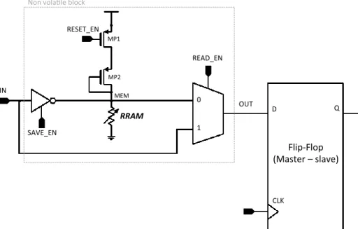
Proposed RNVFF solution relies on the implementation of a non-volatile memory (NVM) block connected to the input of a conventional master-slave Flip-Flop. As illustrated Fig. 6 the NVM block is composed of routing components (input tri-states inverters and output multiplexer). In between lies a branch that connects a central point (MEM) to VDD through two serial PMOS (MP1 and MP2) on
one hand and to ground through a ReRAM memory cell on the other hand. It has to be noticed that the area of this latter branch is reduced since ReRAM element may be processed in the back-end of line on the top of CMOS level. The input tri-states inverter enables connecting and isolating the central point (MEM) to the input of the structure (IN). PMOS transistors of this inverter are adequately sized to provide a current limitation through the ReRAM element when connecting the input IN to the central point MEM. The two inputs multiplexer enables bypassing NVM block, when the signal READ_EN = ‘1’, otherwise (READ_EN = ‘0’) the output of the NVM block is connected to the input (D) of the Flip-Flop. It is worth noting that in most of SoC, Flip-Flops integrate a scan
test feature with a multiplexer on their input. Therefore the multiplexer of the NVM block could be mixed with the scan – multiplexer to introduce a minimal delay overhead.
To summarize, the structure of the NVM block is very simple with two routing elements (input tri-states inverter and output multiplexer) and a branch with two transistors and one ReRAM element (i.e. 2T/1R structure). Considering that the output multiplexer may be mixed with a scan multiplexer, the area overhead introduced by the structure is one tri-states inverter and a 2T/1R branch.
3.3 Save and restore processes description
To save and restore Flip-Flop content, four successive operating modes are required: The normal mode in which the Flip-Flop works in a conventional manner; The save mode in which Flip-Flop content is saved in NVM block;
The read mode in which NVM block content is restored in the Flip-Flop;
The reset mode in which ReRAM memory cell turns back to a high resistance state while the Flip-Flop works in a conventional way.
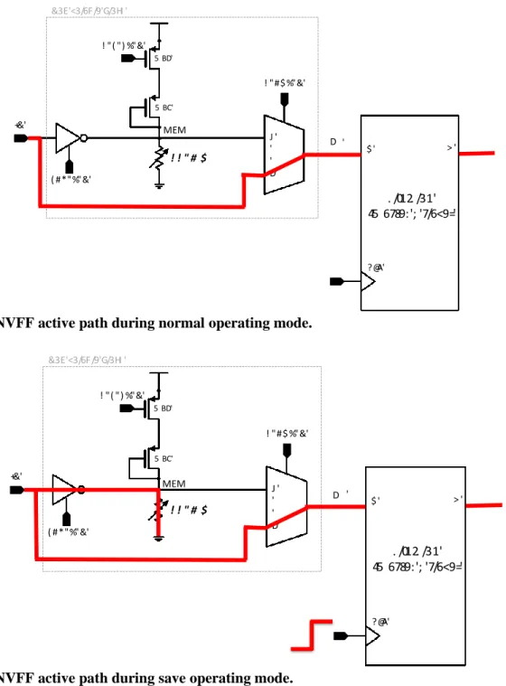
Active path in normal operating mode is illustrated by solid red line in Fig. 7. In this mode the ReRAM cell is isolated from the input (IN) of the structure thanks to the input tri-states inverter, which is open (SAVE_EN = ‘0’). It has to be mentioned, that in this operating mode, the ReRAM cell remains in its initial high resistance state (i.e. HRS). The Flip-Flop works in a conventional manner by connecting the input (IN) of the structure to the input (D) of the Flip-Flop thanks to the output multiplexer (READ_EN = ‘1’). The delay overhead introduces is due to the extra-load of the tri-states input inverters and the routing through the output multiplexer.
Again, the actives paths of the save operating mode are illustrated by the solid red line in Fig. 8. In this mode the ReRAM cell is connected to the input (IN) of the structure thanks to the input tri-states inverter, which is turned on (SAVE_EN = ‘1’). The MEM central point is now the complement of the input (IN) value. When the tri-states inverter is activated, the ReRAM cell is switched to its low
resistance state LRS (IN = ‘0’ and MEM = ‘1’) or remains in a high resistance state HRS (IN=’1’ and MEM=’0’). The Flip-Flop continues to work in a conventional manner and store the value of the input (IN) thanks to the output multiplexer (READ_EN = ‘1’). So during the save mode, the ReRAM resistance state reflects the value of the Flip-Flop. Logic ‘1’ corresponds to a high resistance state whereas logic ‘0’ corresponds to a low resistance state. Right after the save mode, the Flip-Flop can be completely powered-down since ReRAM cell stores the information.
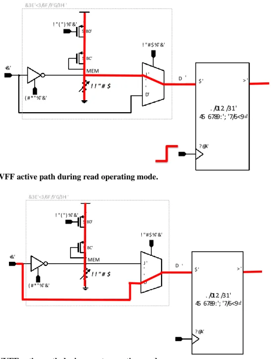
After power-up, a read mode is mandatory to restore Flip-Flop content. Active path in read operating mode is illustrated in Fig. 9. In this mode, the output multiplexer (READ_EN = ‘0’) enables connecting the MEM node to the input (D) of the Flip-Flop, while a clock edge restores the content of the Flip-Flop. The resistive bridge (voltage divider) composed by MP1 (turned-on with RESET_EN = ‘0’) and MP2 on one side and the ReRAM cell on the other side determines the voltage on the node MEM. If the ReRAM cell is in its LRS state then the MEM voltage is grounded and a ‘0’ is restored in the Flip-Flop. In contrast, if the MEM voltage is closed to VDD, a ‘1’ is
restored in the Flip-Flop. MP2 is introduced in the branch to limit the voltage on the node MEM when close to VDD in order to initiate the switching of the ReRAM cell to a HRS state during the read
mode, if needed (ReRAM cell in a LRS state).
Active paths of the reset operating mode are illustrated in Fig. 10. In this mode, the Flip-Flop works again in a conventional way thanks to the output multiplexer that connects the input (IN) of the structure to the input of the Flip-Flop (READ_EN = ‘1’). Doing so, the ReRAM cell is isolated from the rest of the circuit and can turn back to a HRS state, if needed, thanks to the application of a voltage close to VDD through MP1 (turned-on with RESET_EN = ‘0’) and MP2. When RESET_EN =
‘1’, the reset process is stopped and the whole structure turns back to a normal operating mode. 3.4 Conclusion
In conclusion, it is important to note that the standard functionality of the Flip-Flop is guaranteed in all modes, except during read mode. Moreover, the ReRAM state is HRS in all modes when the
content to save is ‘1’ with a minimal leakage current consumption. When the content to save is ‘0’ then the current consumption is restricted to the save, read and reset modes with the switching of the ReRAM cell from HRS to LRS and respectively from LRS to HRS. It is also important to underline that no biasing is necessary during power-off to preserve ReRAM state.
4 RNVFF
S
IMULATIONR
ESULTSTo validate the RNVFF functionality, the full structure is simulated under electrical simulator using a low power CMOS 65 nm design kit and the unipolar ReRAM compact model fitted on best in class literature data. VDD is nominal for the technology and set to 1.2 V during all operating modes except
during power-off where it is set to 0 V. All operating modes are simulated for input values of ‘1’ and ‘0’. MP2 has a minimal length (L=0.06 µm) and a double width (W=0.24 µm) and MP1 has minimal dimensions (L=0.06 µm and W=0.12 µm). The tri-states inverter is composed of NMOS and PMOS transistors with a double length (L=0.12 µm) to limit current during set process and standard width (WPMOS=0.15 µm, WNMOS=0.12 µm). The output multiplexer and the Flip-Flop are standard-cells
from the library.
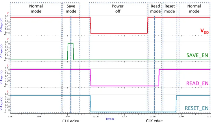
Fig. 11 presents the chronograms of VDD and control signals, i.e. SAVE_EN, READ_EN and
RESET_EN. During the full simulation time of 35 ns, all operating modes are successively simulated,
i.e. normal mode, save mode, power-off, read mode, reset mode and again normal mode.
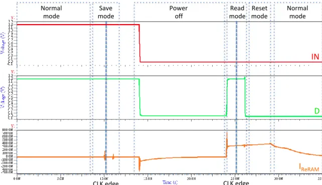
Fig. 12 shows the chronograms of the input (IN) , the Flip-Flop input (D) and the current through the ReRAM cell (IReRAM) to save and restore a logic ‘0’. As described in the previous section, the
ReRAM is set during the save mode with a current of 12 µA during 2 ns. During the read and reset modes, the ReRAM is reset during 5 ns with a current decreasing from 9 µA to 0 µA. During the read mode, the input IN is set to ‘1’ while the read process forces a ‘0’ value at the input D of the Flip-Flop, validating successfully the save and restore processes for a data equal to ’0’.
Fig. 13 shows the chronograms of the input (IN), the Flip-Flop input (D) and the current through the ReRAM cell (IReRAM) to save and restore a logic ‘1’. As previously described, the ReRAM cell
remains in HRS during the save mode with a current below 0.1 µA during 2 ns. During the read and reset modes, the ReRAM cell remains in HRS during 5 ns with a current decreasing from 0.4 µA to 0 µA. During the read mode, the input IN is set to ‘0’ while the read process enforces a ‘1’ value at the input D of the Flip-Flop, validating successfully the save and restore processes of a data equal to ‘1’.
In conclusion, the simulation results validate successfully the functionality of the RNVFF in all operating modes. The simulation also demonstrates that the current consumption of this structure is restricted to the save and restore processes of a logic ‘0’. Indeed, the ReRAM cell remains always in HRS, when the data to save and restore is equal to ‘1’.
5 C
ONCLUSIONIn this paper, a new architecture of non-volatile Flip-Flop based on unipolar Resistive RAM is proposed. This latter architecture is dedicated to power-down applications, in which the content of the Flip-Flop is saved as resistance states in a ReRAM device before power-down and restored after power-up. The overall save and restore processes are detailed together with the architecture of the proposed structure. One may notice that this architecture relies on a non-volatile memory block inserted at the front of a Flip-Flop. The first advantage of such a structure is a better compatibility between the ReRAM memory element and the CMOS level as compared to MRAM or FeRAM-based solutions. Moreover, the use of such a structure does not require any biasing during power-off in comparison to retention Flip-Flop employing a balloon latch. Another point to underline is the low power consumption during all operating modes, except when the cell is set or reset (corresponding to save and read/reset of a ‘0’ content). Finally, the full structure is successfully validated with electrical simulation using a 65 nm CMOS design kit and the unipolar compact model calibrated on best in class data from the literature.
R
EFERENCES[1] V. Kursun, et al., Multi-Voltage CMOS Circuit Design, John Wiley & Sons Ltd. (2006). [2] G. Sery, et al., “Life is CMOS: Why chase life after?”, Proceedings of the IEEE/ACM
International Design Automation Conference, June (2002), pp.78–83.
[3] J. Robertson, “High dielectric constant gate oxides for metal oxide Si transistors”, Rep. Prog. Phys. (2006), vol. 69, no. 2, pp. 327–396.
[4] H. Jiao, et al., “Low-Leakage and Compact Registers with Easy-Sleep Mode”, J. Low Power Electronics (2010), vol. 6, pp. 1–17.
[5] Y. Matsuya, et al., “A 1-V high-speed MTCMOS circuit scheme for power-down application circuits”, IEEE J. Solid-State Circuits (1997), Vol. 32, pp. 861–869.
[6] J. Yan et al., “A design of ferro-DFF for non-volatile systems”, Integrat. Ferroelec., (2006), vol. 81, no. 1, pp. 207–215.
[7] J. Wang, et al., “A Compare-and-write Ferroelectric Nonvolatile Flip-Flop for Energy-Harvesting Applications”, Proc. International Conference on Green Circuits and Systems, (2010), pp. 646–650.
[8] W. Zhao, et al., “Spin-MTJ based Non-Volatile Flip-Flop”, Proceedings IEEE International Conference on Nanotechnology (2007), pp. 399–402.
[9] Y. Guillemenet, L. Torres, G. Sassatelli, and N. Bruchon, “On the use of magnetic RAMs in field-programmable gate arrays”, Int. J. Reconfigurable Computing (2008), pp. 1–9.
[10] S. Yamamoto, et al., “Nonvolatile delay Flip-Flop based on spin-transistor architecture and its power-gating applications”, Japanese Journal of Applied Physics, (2010), vol. 49, no. 9, pp. 090204 (1–3).
[11] W. Robinett, et al., “A memristor-based nonvolatile latch circuit”, Nanotechnology, (2010), vol. 21, pp. 235203 (1–6).
[12] D.C. Kim, et al., “Electrical observations of filamentary conductions for the resistive memory switching in NiO films”, Appl. Phys. Lett. (2006), vol. 88, pp. 202102(1–3).
[13] K. Tsunoda, et al., “Low Power and High Speed Switching of Ti-doped NiO ReRAM under the Unipolar Voltage Source of less than 3 V”, Proc. IEEE Int. Electron Devices Meeting Tech. Dig. (2007), pp. 767–770.
[14] R. Bruchhaus, et al., “Memristive Switches with Two Switching Polarities in a Forming Free Device Structure”, MRS Symposium Proceedings (2011), vol. 137, pp. mrss11-1337-q08-03. [15] M. Bocquet, et al., “Self-consistent physical modeling of set/reset operations in unipolar
resistive-switching memories”, Appl. Phys. Lett. (2011), vol. 98, 263507(1–3).
[16] U. Russo, et al., “Self-Accelerated Thermal Dissolution Model for Reset Programming in Unipolar Resistive-Switching Memory (ReRAM) Devices”, IEEE Transaction on Electron Devices (2009), vol. 56, pp. 193–200.
[17] A.J. Bard, et al., “Electrochemical Methods: Fundamentals and Applications”, Wiley and Sons (2001).
[18] C. Cagli, et al., “Evidence for threshold switching in the set process of NiO-based ReRAM and physical modeling for set, reset, retention and disturb prediction”, IEEE Int. Electron Devices Meeting Tech. Dig. (2008), pp. 301–304.
[19] M.-J. Lee, et al., “2-stack 1D-1R Cross-point Structure with Oxide Diodes as Switch Elements for High Density Resistance RAM Applications”, Proc. IEEE Int. Electron Devices Meeting (2007), pp. 771–774.
[20] F. Nardi, et al., “Control of filament size and reduction of reset current below 10 μA in NiO resistance switching memories”, Solid-State Electronics (2011), vol. 58, pp. 42–47.
F
IGURES ANDT
ABLESFigure 1. Architecture of a classical balloon latch used with power-gating technique (redrawn from
[5]).
Figure 2. Flip-Flop architecture with a back-up module based on FeRAM memory for energy harvesting application (redrawn from [7]).
Figure 3. Architecture of a latch with a non-volatility capability based on two magnetic tunnel junctions MTJ (redrawn from [8]).
(a) (b) (c)
Figure 4. Experimental I(V) characteristics measured on a NiO-based memory structure reported in (a) [18], (b) [19], and (c) [12] and corresponding simulations using the presented ReRAM physical model.
0.0 0.5 1.0 1.5 0 1x10⁻³ 2x10⁻³ 3x10⁻³ 4x10⁻³ 0.0 0.5 1.0 1.5 10 -7 10-6 10-5 10-4 10-3 I Ce ll (V) VCell (V) ISet IReset [18]
Simu. this work
VCell (V)
ISet IReset
[19]
Simu. this work
0.0 0.2 0.4 0.6 0.8 1.0 10-7 10-6 10-5 10-4 10-3 I C e ll (A) VCell (V) Symbols: [12] Lines: Simulations
Figure 5. Maximum current during the reset operation (IReset) as a function of the maximum current
during the preceding set operation (ISetMax). Experimental data were extracted from [20].
Figure 6. RNVFF architecture with Non-volatile block based on ReRAM cell connected to the Flip-Flop input D. 10-6 10-5 10-4 10-3 10-2 10-6 10-5 10-4 10-3
10-2 Symbol : Data [Nardi10-SSE]Line : Simu.
I res
e
t
(A)
Figure 7. RNVFF active path during normal operating mode.
Figure 8. RNVFF active path during save operating mode.
! "#$ %"&' ! "( ") %"&' ( #*"%"&' +&' , - ) ' . /012. /31' 45 6789:'; '7/6<9=' $ ' > ' ?@A' ! ! " # $ 5 BC' 5 BD' &3E'<3/6F /9'G/3HI ' J ' ' ' D' D MEM ! "#$ %"&' ! "( ") %"&' ( #*"%"&' +&' , - ) ' . /012. /31' 45 6789:'; '7/6<9=' $ ' > ' ?@A' ! ! " # $ 5 BC' 5 BD' &3E'<3/6F /9'G/3HI ' J ' ' ' D' D MEM
Figure 9. RNVFF active path during read operating mode.
Figure 10. RNVFF active path during reset operating mode.
! "#$ %"&' ! "( ") %"&' ( #*"%"&' +&' , - ) ' . /012. /31' 45 6789:'; '7/6<9=' $ ' > ' ?@A' ! ! " # $ 5 BC' 5 BD' &3E'<3/6F /9'G/3HI ' J ' ' ' D' D MEM ! "#$ %"&' ! "( ") %"&' ( #*"%"&' +&' , - ) ' . /012. /31' 45 6789:'; '7/6<9=' $ ' > ' ?@A' ! ! " # $ 5 BC' 5 BD' &3E'<3/6F /9'G/3HI ' J ' ' ' D' D MEM
Figure 11. Chronograms of control signals and VDD during the save & restore processes using a RNVFF.
Figure 12. Chronograms of data signals and ReRAM current during the save & restore processes using a RNVFF, with IN=’0’.
V
DDSAVE_EN
READ_EN
RESET_EN
Normal mode Save mode Power off Read mode Reset mode Normal mode CLK edge CLK edge IN D IReRAM Normal mode Save mode Power off Read mode Reset mode Normal mode CLK edge CLK edgeFigure 13. Chronograms of data signals and ReRAM current during the save & restore processes using a RNVFF, with IN=’1’. IN D IReRAM Normal mode Save mode Power off Read mode Reset mode Normal mode CLK edge CLK edge
B
IOGRAPHIESJ.M. Portal received a M.S. degree in Electrical Engineering and a Ph.D. degree in Microelectronics
from the University of Montpellier, France, in 1995 and 1999 respectively. He is currently Professor at the Aix-Marseille University, and manages, since 2009, the “Memories Team” of the IM2NP (Institute of Materials Microelectronic and Nano-sciences of Provence—France). His research interests include the various aspects of design, design for manufacturing and test of logic and memory circuits, including FPGA, charge trap as well as emergent memories. He has published more than 60 papers (journal and conference) on these fields.
M. Bocquet received his M.S. (Electrical Engineering) degree in 2006 and his Ph.D. (Electrical
Engineering) degree in 2009, both from the University of Grenoble, France. He is currently associate professor in the Institute of Materials, Microelectronics and Nano-sciences of Provence (IM2NP - University of Provence, France). His research interests include memory model, memory design, characterization and reliability.
D. Deleruyelle received his M.S. (Electrical Engineering) degree in 2001 and his Ph.D. (Electrical
Engineering) degree in 2004, both from the University of Grenoble, France. He is currently associate professor in the Institute of Materials, Microelectronics and Nano-sciences of Provence (IM2NP - University of Provence, France). His research interests include emerging memories model, and physical and electrical characterizations.
C. Muller received the Ph.D. degree in 1996, from the University Joseph Fourier in Grenoble, France.
His Ph.D. thesis was focused on fast oxygen ion conductors for application in gas sensors and solid oxide fuel cells. In 1997, he joined L2MP at the University of South Toulon Var (France) for developing studies on phase transitions in ferroelectrics and field-induced reorientation of
ferroelectric domains. He managed the ferroelectrics group in L2MP during several years and initiated research activities on integrated ferroelectric thin films for memory applications (FRAM) in a close industrial partnership. He was nominated as Full Professor in 2003 and joined the University of Provence in Marseille in September 2007. Last five years, he contributed to several European projects focused on emerging non-volatile memory technologies (FRAM, MRAM, RRAM...) with a specific interest on programming physical mechanisms and reliability performances.
![Figure 2. Flip-Flop architecture with a back-up module based on FeRAM memory for energy harvesting application (redrawn from [7] ).](https://thumb-eu.123doks.com/thumbv2/123doknet/14636221.734872/16.918.297.644.625.889/figure-architecture-module-feram-memory-harvesting-application-redrawn.webp)
![Figure 4. Experimental I(V) characteristics measured on a NiO-based memory structure reported in (a) [18], (b) [19], and (c) [12] and corresponding simulations using the presented ReRAM physical model.](https://thumb-eu.123doks.com/thumbv2/123doknet/14636221.734872/17.918.142.799.493.820/experimental-characteristics-measured-structure-reported-corresponding-simulations-presented.webp)